PROTOTYPE IMAGING CD-ZN-TE ARRAY DETECTOR
P. F. BLOSER1, T. NARITA1, J. E. GRINDLAY1, K. SHAH2
1Harvard-Smithsonian Center for Astrophysics, Cambridge, MA 02138
2Radiation Monitoring Devices, Inc., Watertown, MA 02172
ABSTRACT
We describe initial results of our program to develop and test Cd-Zn-Te (CZT) detectors with a pixellated array readout. Our primary interest is in the development of relatively thick CZT detectors for use in astrophysical coded aperture telescopes with response extending over the energy range keV. The coded aperture imaging configuration requires only relatively large area pixels (1-3 mm), whereas the desired high energy response requires detector thicknesses of at least 3-5 mm. We have developed a prototype detector employing a 10 x 10 x 5 mm CZT substrate and 4 x 4 pixel (1.5 mm each) readout with gold metal contacts for the pixels and continuous gold contact for the bias on the opposite detector face. This MSM contact configuration was fabricated by RMD and tested at Harvard for uniformity, efficiency and spatial as well as spectral resolution. We have developed an ASIC readout (IDE-VA-1) and analysis system and report results, including % (FWHM) energy resolution at 60 keV. A prototype design for a full imaging detector array is discussed.
INTRODUCTION
The field of X-ray and gamma-ray astronomy has been limited since its beginnings by the somewhat primitive state of high energy radiation detector technology, especially imaging technology. Particularly in the hard X-ray energy range ( keV), creating imaging instruments is difficult, since energies are too high for multi-layer focusing optics ( 80 keV) and too low for Compton telescopes ( 500 keV). The optimum method for imaging in this range is the coded aperture technique, in which a specially-designed mask casts a shadow on a position-sensitive detector from which the position of the X-ray source can be deduced. Though successfully employed in many experiments, this method has been limited by the poor spatial resolution of the scintillation detectors (NaI, CsI, etc.) used to date. A solid-state detector with small pixels would improve the spatial resolution immensely. Scintillators also have poor energy resolution compared to solid-state, semiconductor devices. Thus hard X-ray astronomy is in need of large area, room temperature, semiconducting imaging detectors with good energy resolution.
Recently, Cadmium-Zinc-Telluride (CZT) has shown great promise in meeting this need. Alloying CdTe with Zn increases resistivity [1], allowing higher bias voltage without increased leakage current. CZT has high stopping power and a wide bandgap, but can suffer from poor charge collection due to deep traps and poor mobility-lifetime () products for holes. However, it has been found [2] that employing a grid of pixels small relative to the detector thickness creates an internal electric field favorable for the collection of only one polarity of charge carrier; if used to collect electrons, the easily-trapped holes are no longer important (this is often called the small pixel effect). As this is precisely the detector geometry required for hard X-ray telescope detectors, pixellated arrays of CZT have enjoyed intense scrutiny in recent years [3-6]. Here we describe initial results of our program to develop imaging CZT array detectors specialized for use in a hard X-ray survey telescope.
EXPERIMENT
Our detector development work has been motivated by a hard X-ray survey telescope concept such as the previously proposed MIDEX mission EXIST [7]. The purpose of such a mission is to conduct an all-sky survey with high sensitivity and resolution (spatial and spectral) from keV; therefore, the telescope must have a large field of view with thick ( mm) CZT detector elements. Both these considerations lead us to a pixellated detector design. Since relatively defect-free CZT crystals are currently most readily available in mm sizes, we are led naturally to a unit detector element of mm with a array of 2.5 mm pixels spaced by 0.5 mm. These could be grouped into a array, which we call a basic detector element (BDE), and read out by a single 64 channel preamp-shaper-multiplexer Application Specific Integrated Circuit (ASIC) with self-triggering and low power consumption. These BDEs can then be tiled into a large array.
A different approach is a strip detector, with perpendicular strips on opposite sides to record x and y positions from electrons and holes [4][5]. While strip detectors require fewer channels (2N) for readout than do pixel (N2) detectors, they have the disadvantage of requiring collection of both electrons and holes to record x and y positions; this limits their thickness and thus their high energy response. Also, strips are generally much longer than pixels and thus have higher capacitance and noise. Finally, the large field of view combined with the large thickness requires large detector elements to minimize charge spreading effects. For example, for the field of view of EXIST and a 5 mm thick detector, the pixels must be mm across to ensure the charge spreads no further than the nearest neighbor pixel. Such large pixels allow us to cover a big collecting area with relatively few pixels which can be readily coupled to multi-channel ASIC readouts.
Therefore, we are conducting extensive development and testing of thick pixellated CZT detectors and multi-channel ASICs. Our immediate goal is to construct a BDE and fly it on a scientific balloon in order to measure background and uniformity of response under space flight conditions. As a part of this effort RMD Corp. has fabricated a mm detector out of high pressure Bridgman counter grade CZT obtained from eV Products, depositing a array of 1.5 mm gold pixels spaced by 0.2 mm on one side and a continuous gold contact on the other. A 1.5 mm wide gold “guard ring” surrounds (0.2 mm gap) the pixel array and was maintained at ground potential.
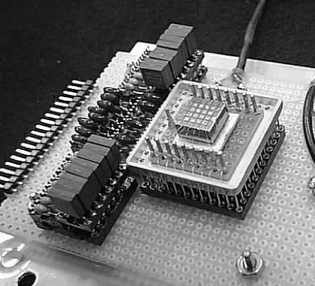
At CfA, we have tested this detector for spatial and spectral resolution using a 241Am source of 60 keV X-rays. The detector was read out by two 8 channel VA-1 preamplifier ASICs provided by IDE AS Corp. The CZT is irradiated through the metal-ceramic chip carrier on the side with the continuous contact, which is negatively biased, so that the electrons drift nearly the entire 5 mm thickness to the grounded pixels. Gold wires from the chip carrier holding the detector are connected to the pixels with silver epoxy. The chip carrier sits on a small board providing decoupling capacitors and bias resistors for each channel (cf. Figure 1); this board in turn plugs into a test board provided by IDE AS Corp. that carries the ASICs and provides line drivers for each output channel. This board was not optimized for minimal capacitance, as indicated below. A lab pulser was input through 1.4 pf capacitors into each ASIC channel in parallel with the detector. Spectra were then recorded one channel at a time on a lab PC with a commercial MCA card. The MCA triggered internally on the shaped pulse; we also experimented with deriving a trigger pulse from the cathode of the detector (via a separate preamp) and got the same results. The 241Am source was mounted on a computer-driven translation table allowing collimated X-rays to be scanned across the detector with mm resolution. A photograph of the RMD detector is shown in Figure 1.
RESULTS
The VA-1 ASIC linearity is shown in Figure 3. Voltage pulses from the lab pulser were put into a 1.4 pF capacitor, in parallel with the CZT input, and the peak channel recorded in the lab MCA. A shaping time of 1 s was used. This range of input voltages corresponds roughly to 30-180 keV in our CZT detector, and the ASIC is found to be linear over this range. We were limited to this range by our MCA, but the ASIC should be linear up to 600 keV.


We measured the leakage current as a function of bias voltage for each pixel using a Keithley 237 high voltage source and current meter. The bias voltage was stepped from -500 V to 500 V and back down in 50 V steps. The detector was uniform in this respect; a typical I-V curve is shown in Figure 3. At our typical operating bias voltage of -500 V, the leakage measured current is about 19 nA. We calculate the resistivity of the detector to be -cm.
Spectra of 60 keV X-rays from a 241Am source were taken with the lab MCA for all pixels. The bias voltage was -500 V, the shaping time was 1 s, and the MCA was operated in a self-triggered mode to obtain spectra of individual channels. We also recorded spectra with the MCA triggered by a pulse from the negatively-biased continuous electrode, and obtained the same results. First, spectra were taken with the detector fully illuminated and a pulser injected simultaneously into all channels to monitor electronic noise. We obtained good spectra for all 16 pixels, as shown in Figure 4.

The low energy cutoff in these spectra is keV; the low energy Am and Np lines are not visible in any case because the detector is illuminated through the metal-ceramic chip carrier. There was some variation in the gains of the 16 channels due to differences in the line drivers on the IDE AS test board. The 60 keV line was fit with a combination of a gaussian and low energy exponential tail to model the effects of charge trapping or incomplete charge collection between pixels, as shown in Figure 5.

We define the photopeak efficiency as the ratio of the counts in the gaussian to the total counts in the gaussian plus tail, and the energy resolution as the ratio of the FWHM of the gaussian to the peak energy. We found typical photopeak efficiencies of 75% for the 60 keV line, and the energy resolution varied from %. Most of this peak width is due to electronic noise, as evidenced by wide pulser peak widths. As discussed below, the primary contribution to the noise is probably stray capacitance in our detector carrier board, which we know varies from channel to channel with the lengths of the wires. We have subtracted the pulser peak width in quadrature from the X-ray line width to estimate the intrinsic detector energy resolution of %. The pixel to pixel variation in resolution is shown in Figure 7.


Some of this variation is still probably due to channel to channel capacitance variations. The good photopeak efficiency and energy resolution indicate that the detector is working in the small pixel regime.
Next we collimated the beam from the 241Am source to form a mm spot size on the detector and moved it from pixel to pixel with the translation table. The recorded spectrum of the collimated beam on a central pixel is shown in Figure 7. The low energy tail is practically gone; the photopeak efficiency is 97%. The energy resolution (with pulser width subtracted) is 3.8%. We took spectra of adjacent pixels to investigate the effects of charge spreading. The four surrounding pixels showed no counts above background, indicating that charge spreading is localized to one pixel even in a 5 mm thick detector. Our spatial resolution is thus much finer than our 1.5 mm pixels. We scanned the collimated beam onto the 0.2 mm interpixel region and recorded a spectrum from the adjacent pixels. We find here a photopeak efficiency of 70%, indicating that the low energy tails originate mostly from photons incident between pixels, which naturally results in charge division between pixels.
We have investigated the various sources of noise in our detector and readout system by adding components one at a time and observing the change in the pulser peak width. The noise sources are assumed to add in quadrature. We find a baseline noise of the IDE AS preamp test board and the bare readout card with the detector not in place of . The VA-1 ASIC has a noise of pF of input capacitance. This would indicate we have about noise or 19 pF of stray capacitance in our detector carrier card and the IDE AS test board. Also, we find from the AC coupling capacitors and from the bias resistors. Additional noise contributions are from the detector (chip carrier) capacitance and from leakage current. We are currently making a printed circuit board detector carrier card that should reduce the stray capacitance significantly.
CONCLUSIONS
We have presented preliminary results from our program to develop thick pixellated CZT array detectors with ASIC readouts. For 60 keV radiation incident within a pixel, the energy resolution and photopeak efficiency of individual pixels are % and 97%, respectively. There is no cross-talk due to charge spreading between pixels, and the small pixel effect is clearly demonstrated by the near absence of a low energy tail. (Some effect due to charge trapping may become evident when the electronic noise is reduced, however.) The VA-1 ASIC performs well, showing low noise and good linearity. Our immediate plans include the completion of a 16 channel parallel readout system interfaced to a compact single board computer, which will allow true imaging operation, and investigation of new self-triggering ASICs with up to 64 channels to allow for larger arrays. Balloon flight tests of a prototype BDE array and coded aperture telescope are planned.
This work was supported in part by NASA grant NAG5-5103.
REFERENCES
1. J. Butler, C. Lingren, F. Doty, Trans. Nuc. Sci. 39, 605 (1992).
2. H. Barrett and J. Eskin, Phys. Rev. Let. 75, 156 (1995).
3. A. Parsons, C. Stahle, C. Lisse, S. Babu, N. Gehrels, B. Teegarden, P. Shu, Proc. SPIE 2305, 121 (1994).
4. C. Stahle, Z. Shi, K. Hu, S. Barthelmy, S. Snodgrass, L. Bartlett, P. Shu, S. Lehtonen, K. Mach, Proc. SPIE 3115, 90 (1997).
5. J. Matteson, W. Coburn, F. Duttweiler, W. Heindl, G. Huszar, P. Leblanc, M. Pelling, L. Peterson, R. Rothschild, R. Skelton, Proc. SPIE 3115, 160 (1997).
6. T. Tumer, T. O’Neill, K. Hurley, H. Ogelman, R. Paulos, R. Puetter, I. Kipnis, W. Hamilton, R. Proctor, in The Transparent Universe (Proc. 2nd INTEGRAL Workshop, St. Malo, France, 1996) pp. 361-365.
7. J. Grindlay, T. Prince, N. Gehrels, J. Tueller, C. Hailey, et al., Proc. SPIE 2518, 202 (1995).