For further information contact Chao-Lin Kuo, e-mail: clkuo@astro.caltech.edu
Antenna-Coupled TES Bolometers for CMB Polarimetry
Abstract
We have developed a completely lithographic antenna-coupled bolometer for CMB polarimetry. The necessary components of a millimeter wave radiometer — a beam forming element, a band defining filter, and the TES detectors — are fabricated on a silicon chip with photolithography. The densely populated antennas allow a very efficient use of the focal plane area. We have fabricated and characterized a series of prototype devices. We find that their properties, including the frequency and angular responses, are in good agreement with the theoretical expectations. The devices are undergoing optimization for upcoming CMB experiments.
keywords:
cosmic microwave background, polarization, millimeter wave instrumentation1 Introduction
The primary science goals of the next generation Cosmic Microwave Background (CMB) polarization experiments are to produce a high fidelity E-mode power spectrum and to search for the B-mode polarization. A detailed E-mode spectrum will help constrain the cosmological parameters, and test crucial hypothesis in standard cosmology. The measurements of B-mode polarization at high multipole value () can be used to study the matter power spectrum through gravitational lensing. At low , B-mode polarization can only be produced by gravitational waves. The detection of this signature would provide invaluable information on the fundamental physics in the very early Universe, such as the energy scale of Inflation. To achieve these goals in the presence of the astronomical foregrounds, the instruments will require wide frequency coverage, a large number of sensitive microwave detectors, and exquisite control of systematics[1].
Bolometers can provide photon noise-limited sensitivity over a wide frequency range. However, the existing feedhorn-coupled micromesh bolometers [2, 3, 4] face difficulties in extending the frequency coverage and scaling to kilo-pixel instruments. The micromesh bolometers with low thermal conductance (both the “spiderweb”[2] and the “PSB”[4] type) have currently been demonstrated with architectures suitable for frequencies 60 GHz. The metallic corrugated feedhorns used for beam collimation are heavy and expensive to implement in systems with thousands of pixels at cryogenic temperatures. Semiconductor bolometers with high impedances ( ) pose a challenge for kilo-pixel readout. Each of the bolometers requires one impedance-matching JFET, which dissipates significant amount of electrical power. The noise contribution from standard JFET is prohibitively large for use in multiplexers. So far, the number of elements in a semiconductor bolometric receiver is limited to a few hundreds [3].
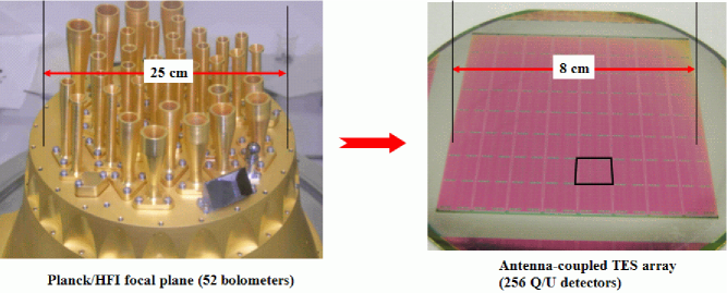
We describe a CMB polarimeter based on antenna-coupled superconducting transition edge sensors (TES) that can avoid all these difficulties. In this design, the beam forming slot-antenna array, microstrip band defining filter, and TES detectors are fabricated on a silicon chip. These completely photolithographic detectors provide intrinsic polarization sensitivity and purity, collimated beams, simultaneous measurement of Stokes I and Q parameters in a single spatial pixel, high focal-plane packing density, and massively parallel fabrication. The migration from semiconductor bolometers to superconducting TES bolometers enables the readout of thousands of pixels with moderate electronics complexity. This is achieved by superconducting quantum interference device (SQUID) multiplexers [5, 6]. In a microstrip-coupled bolometer, only the mechanically robust slot antenna scale with wavelength, therefore the entire frequency range ( 30 GHz to 500 GHz) of interest in CMB science can be covered by the same technology.
The densely populated antennas allow a very efficient use of the focal plane area. The excellent uniformity of the photolithography provides intrinsically good alignment and orthogonality of the two polarization modes, uniformity of the in-line filter band-passes, and gain matching of all elements for two orthogonal polarizations. Besides TES, the microwave antenna-coupled architecture is completely compatible with other detector technology, such as indium bump-bonded NTD chips and microwave kinetic inductance detectors.
The paper is organized as follows. We describe the components of a polarization sensitive antenna-coupled bolometer in §2. The design, fabrication, and measured optical properties of prototype detectors are presented in §3. Issues related to the implementation of arrays of antenna-coupled bolometers in a polarization receiver are discussed in §4, including a comparison of on-chip polarization modulators and half-wave plates (§4.2). We describe our detector development plan and several proposed CMB polarization experiments that will be using this technology in §5.
2 The Components of a Polarization Detector
2.1 In-phase planar slot antenna
A beam forming element limits the radiation background on the detectors, and reduces side-lobes, stray light coupling, and sensitivity to cryogenic temperature fluctuations. Feed-coupled bolometers are especially advantageous compared to bare arrays under low background loading conditions at millimeter wave frequencies [7, 8]. In an antenna-coupled detector, a planar array of slot antennas perform the function of beam collimation. The signals coming from the sub-antennas are combined coherently by a summing network to form a beam.
Long slots in a ground plane are intrinsically polarization sensitive since microwave radiation tends to excite electric fields across the slots. Another key motivation for choosing a slot architecture is that most of the substrate remains metalized, shielding the summing tree network from the incoming radiation. We have developed 2 types of polarization selective planar antenna. The first one is a broad-band single polarization slot antenna [9, 10]. In this design, parallel long slots are patterned in the superconducting niobium ground plane. In each slot, a vertical microstrip summing tree with stub capacitors collects the incoming radiation. A horizontal summing tree subsequently joins the vertical trees and sends the signal to the filter and the bolometer. The second design is a dual polarization antenna, with two colocating orthogonal sets of slots, and two independent microstrip summing trees and TES detectors, each of which measures one linear polarization. Such dual-polarization antenna makes efficient use of the focal plane real estate, and reduces polarization artifacts associated with pointing errors in certain observation modes [1].
There are several research groups involved in the development of microstrip-coupled bolometers. Alternative beam collimation methods include external hyperhemispherical lenses or platelet feeds [11, 12, 1]. The advantages of the photolithographic planar phase-antenna approach are fabrication simplicity, mechanical robustness at cryogenic temperatures, and immunity to misalignment. Compared with the highly curved lenses, the flat silicon entry surface also greatly simplifies the anti-reflection coating.
2.2 The summing network
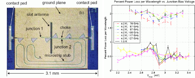
Our array design depends critically on the loss properties of microstrip transmission lines. We conducted measurements of the loss using the open-ended microstrip stub circuit, at 75-120 GHz, 220-320 GHz and 450-550 GHz, at both 4.2 K and 1.5 K. A 75-120 GHz test device is shown in Fig.2. At T = 1.5 K, the loss appears to be dominated by temperature independent loss in the dielectric (SiO). With a loss tangent () , the expected loss at 150 GHz from the entire summing tree is on the order of 10%. Since the loss per propagation wavelength is nearly independent of frequency, and the pixel size scales with wavelength for a fixed F/number, the total loss should not change when we scale this design to other operating frequencies. This low loss figure is qualitatively confirmed in the optical efficiency measurements described in §3.2.
The sidelobe response of the antenna is largely determined by how each sub-antenna is excited by the summing network. In all the current antenna designs, the sub-antenna arranged in a square grid pattern are excited equally by the feed network. Consequently, the radiation pattern exhibits minor sidelobes (at -15dB) and a four-fold symmetry. It is straightforward to improve the symmetry and to reduce the sidelobes by redesigning the feed network to taper the excitation pattern. The microstrip feed network which collects the signals from sub-antennas has to match the impedance of the antennas on one end, while halving its impedance at each binary divider. Tapered impedance transformers are used to maintain the downstream microstrips at a manageable width. We use a combination of SuperMix library[13] and SONNET simulation software to optimize the design of the summing network.
2.3 The microstrip in-line filters
In a feedhorn-coupled bolometric radiometer, long wavelength radiation is rejected sharply by the waveguide cutoff, which is absent in an antenna-coupled bolometer. Fortunately, microstrip in-line filters can be easily integrated with antenna-coupled detectors. From a system point of view, it is in fact desirable to avoid multiple external quasioptical mesh filters, because they tend to generate reflections, resulting in ghost images. The off-axis behavior of metal mesh filters are also not well-studied.
We have developed a lumped-element 3rd order bandpass Chebyshev filter, consisting of CPW inductors and stub capacitors. This compact filter design does not include any “vias” (direct electrical contacts to the ground plane), and is fully compatible with photolithographic processes. Because of their non-resonant nature, these filters do not have fundamental harmonic leaks. The bandgap frequency (690 GHz) of niobium microstrips provides a natural high frequency cutoff for CMB experiments. In future applications, blocking filters are likely to be used for decreasing the thermal loading, while microstrip filters are used to define the science bands.
2.4 The TES bolometer
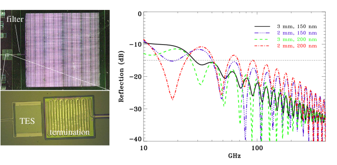
After the bandpass filter, the signal collected by the antenna is transmitted through the Nb microstrip, and readout with microstrip-coupled bolometers, thermally isolated on micro-machined silicon nitride beams. The TES sensor is coupled to a Nb/SiO/Nb microstrip, which enters the thermally isolated patch on a suspended silicon nitride beam, and terminates in a meandering normal-metal microstrip (see Fig.3). A TES film deposited on the isolated region, and readout via superconducting Nb leads, detects the heat from dissipation of electromagnetic energy in the resistor. The bolometer operates in the standard voltage bias configuration, which provides strong electrothermal feedback [14]. The principal benefits of this operating mode are linearity and rapid speed of response.
The termination resistor is made of a meander of normal metal open-ended microstrip. The un-absorbed EM wave is reflected at the end of the microstrip, as a result the effective length of the resistive microstrip is twice the physical length (2.2 mm). Since the characteristic impedance is largely determined by the geometry, the impedances of the superconducting and resistive microstrips are well-matched. The termination efficiency is calculated to be at 100 GHz. The advantages of this design are wide bandwidth and immunity to variations in the thickness and the resistivity of the lossy film. The same meandering microstrip can be used to terminate 30 GHz radiation with an efficiency of . A 3 mm long microstrip will absorb up to of the incoming power (Fig.3). The heat capacity of the gold meander is on the order of or less, small compared to that of the TES film. The detector giving a physical time constant on the order of a few ms for a thermal conductance appropriate for CMB polarimetry. This time constant will be reduced by the factor of the loop-gain in the voltage biased operating condition[14]. Another significant advantage of microstrip-coupled bolometer geometry is that the thermalization time constant is much shorter than the external (bolometer) time constant, providing excellent thermal efficiency [15, 3].
While in theory small-volume bolometers might someday provide lower noise equivalent power (NEP) at a higher physical temperature [16, 17], a micro-machined mechanically-isolated bolometer allows the characteristics of the termination, the thermistor, and the thermal conductance to be optimized independently. State-of-the-art photolithography can now reliably produce silicon nitride legs with extremely high aspect ratio[18]. The NEP required by a space-borne CMB mission is now routinely achieved in the laboratory with appropriate time constant.
The TES sensors will be read out using SQUID current amplifiers with time-domain multiplexing [5] provided by NIST. To demonstrate the compatibility of TES and the NIST MUX, we have fabricated a low thermal conductance, 8 element Mo/Au TES array ( 0.12 K), and integrated it with NIST’s SQUID multiplexing readout. The observed noise degradation from the readout is small: we measured a dark NEP of W.
Time-domain SQUID multiplexing has been under development for a number of years and is now a fairly mature technology. The current SQUID MUX can multiplex up to 32 channels [5]. In the future, the microwave frequency domain SQUID MUX [19] with reflectometer readout might be able to multiplex hundreds or even thousands of detectors, with electronics at a much lower cost.
3 Prototype Detectors
The antenna-coupled architecture has now been fully demonstrated. We have fabricated and thoroughly characterized a series of prototype antenna-coupled TES detectors. We use Mo/Au (100nm/10nm) bilayers as the TES to obtain a transition temperature of 0.9 K, appropriate for high-background optical testing. In the following sections we describe the fabrication, test, and measured optical properties of these prototype detectors.
3.1 Fabrication
The devices are fabricated in the Microdevices Laboratory of the Jet Propulsion Laboratory. The process begins with 200 nm of Nb sputtered onto a 100 mm diameter Si wafer as the ground plane. Slot antennas are then patterned using the reactive ion etching (RIE) process. In order to separate the spectral responses of the antennas and the microstrip filters, half of these prototype detectors are not incorporated with filters. Thermal SiO (400nm) was evaporated on the top of the Nb ground plane. This then becomes the dielectric layer for the microstrips. The TES film dimension is 100 m 95 m, giving a normal resistance of 0.6 . A thin Ti layer (4nm) is used to promote adhesion between the TES and the SiO layer. The TES layer is then ion milled and cleaned using high power oxygen plasma. The absorbing resistor is a Ti/Au/Ti (4nm/150nm/4nm) meander. A second sputtered SiO layer (100nm) is used to protect the resistor layer. The wafer is then sputtered for the Nb microstrip with a thickness of 400nm and etched using the fine contact alignment method. Finally, front-side and back-side silicon nitride membranes are etched, followed by deep-trench Si etch process to form silicon nitride beam-isolated bolometers. In Fig.3, the antenna, the termination resistor, and the TES film (before release) are shown.
3.2 Optical tests and results
3.2.1 Test set-up
The devices are cooled by a closed-cycle 3He refrigerator. A low pass metal mesh filter with a cut-off frequency of 280 GHz is inserted in the optical train for this initial testing. Carbon-loaded PTFE sheet with a thicknesses of 2 millimeters is used to reduce in-band millimeter wave loading on the detectors, providing an attenuation of . Additional Fluorogold, plain PTFE sheets, and metal mesh filters are used for infrared blocking. A quartz plate is glued onto the silicon entry surface as the anti-reflection coating. A superconducting niobium shield with a 4.4-cm opening is placed at 4 K during the measurements to guard the TES and the SQUID read-out against magnetic interference.
For each detector, the angular response is measured with an optically modulated thermal source. The frequency response is measured with a large aperture Fourier transform spectrometer (FTS). The optical efficiency (the normalization of the spectrum) is measured separately by illuminating the detector with a known optical power from a cold blackbody source in the dewar. It is crucial to maintain and monitor the temperature of the detector substrate while heating up the blackbody illuminator, since a systematic drift in the the bath temperature could be mis-interpreted as an optical power. We use a metal mesh filter and a Fluorogold sheet to filter out infrared radiation from the illuminator. We mount an NTD thermistor chip on the detector silicon substrate to monitor the temperature drifts. We observe a temperature rise of mK in the substrate when the illuminator temperature is raised by K. This systematic drift is corrected for in the results reported here.
3.2.2 Radiation pattern
The measured FWHM for both the single- and dual- polarization detectors are , in good agreement with the theoretical predictions and previous measurements with SIS junctions using a coherent source [9, 10]. Out of the 8 antennas measured (4 are shown in Fig.4), 7 produce satisfactory radiation patterns. One dual polarization detector (not shown) exhibits a double-peak mainlobe and sidelobes up to 25%. This can be explained by a broken or shorted microstrip in the summing tree. New fabrication equipments and techniques (see §4.1) will greatly improve the reliability of the summing network in the upcoming batch of detectors.
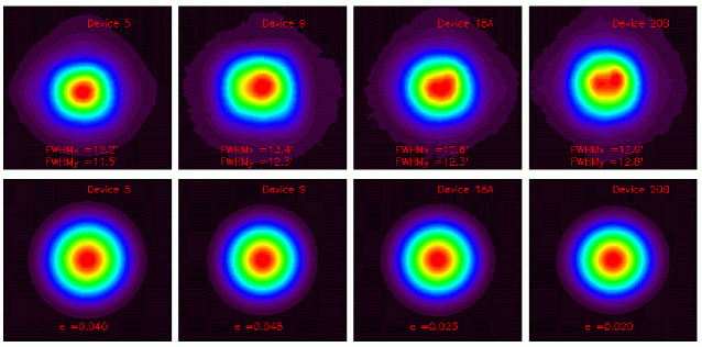
We investigate the asymmetries in the radiation patterns by repeating the measurements after a rotation of the detector. We find that the minor asymmetry near the peak in the radiation pattern is caused by the optical set-up, most likely the infrared filters at oblique angles. The measured cross polarization responses of the antennas are also dominated by the reflections from these infrared filters, at the level for both the single-polarization and dual-polarization antennas. The system is currently being re-designed to allow a more symmetric optical path. With the present set-up, we place an upper limit on the cross-polarization to be less than , and the ellipticity to be less than .
As stated earlier, the radiation pattern of a uniformly excited phased antenna have sidelobes at -15dB level. In the previous measurements with SIS junctions, these sidelobes are observed to be at the predicted level. In our current measurements, the optical opening is not large enough for sidelobe characterization. In a polarization receiver, the sidelobes will be terminated at the cold Lyot stop. The illumination of the pupil, and consequently the beam on the sky, is then determined by the main lobe of the antenna radiation pattern. Neglecting distortions from geometrical optics and assuming the phase errors are small, the beams on the sky can be approximated by the Fourier transform of the illumination patterns. We take the Fourier transform of the measured radiation patterns (Fig.4) with a cold stop at a radius of 1.29 FWHM (corresponding to a “20dB” taper for a Gaussian illumination), to assess the beam shapes expected from a telescope fed by antenna-coupled bolometers. The resulting beams are highly symmetrical and have very low (dB) sidelobe content (bottom rows of Figure 4). We comment on the polarization modulation and beam artifacts in §4.2.
3.2.3 Spectral response and optical efficiency
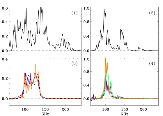
The FTS spectra in Figure(5) are normalized with the blackbody illuminator measurements (Fig.6). The effects of a Mylar beam-splitter is corrected for. We also assume single-moded throughputs () while plotting these spectra. The spectrum of the unfiltered single-polarization device indicates that the long-slot antenna has a bandwidth in excess of (Fig.5, panel 1.). The spectrum shows prominent interference fringes, with optical efficiency lower than expected, especially near the design frequency of 100 GHz. We attribute the anomalously low efficiency and fringes to reflections in the microstrip summing network. To obtain largest possible bandwidth, we chose an array design with feed points. However, a more careful analysis carried out after the array fabrication indicates that the impedance transformer in the summing network causes much higher reflections than originally estimated. This design flaw can easily be fixed in the next generation devices.
The unfiltered dual-polarization antenna shows a sharp resonance at the design frequency of 100 GHz, as well as two additional resonances near 145 GHz and 190 GHz (Fig.5, panel 2.). The main resonance has a peak optical efficiency around 90%, and a usable bandwidth of , agreeing with the theoretical calculations based on method of moments [9]. The summing network in the dual-polarization antenna incurs some reflections, but much less than that from the network.
Comparing the spectrum of the unfiltered single-polarization detector with those of the filtered detectors (Figure 5, panel 3., spectra from two detectors are shown), we find that the microstrip filters have a bandwidth, centering around GHz. Good uniformity is observed in the transmissions of two filters. Overall, the microstrip filters show high out-of-band rejection, and sharp cut-off edges. An external high-pass thick grill filter is used to limit harmonic leaks between 170 GHz and 280 GHz (the cutoff of the metal mesh filter) to be . The filtered dual-polarization detectors (Figure 5, panel 4., spectra from two devices, or four TES, are plotted) tell a similar story. The low frequency end cutoff near 95 GHz is provided by the microstrip filters. The high frequency cutoff at 110 GHz is dominated by the antenna itself, as is apparent by comparing the two right panels.
The center frequency of the microstrip filters is designed to be at 100 GHz, 20% lower than the measured value. To investigate the frequency shift, we measure the thickness of the dielectric layer with a profilometer. The difference between the measured thickness and the target thickness is too small to account for the observed disagreement. Some slight misalignment is observed in these first generation prototype detectors made with contact lithography. We perform numerical calculations for filters with misalignments in different layers (SiO, the Nb microstrip, and ground plane). The effects to the transmission of the filter are again found to be very small. We arrive at the conclusion that the dielectric constant is lower than the target value, presumably because of contaminations during the SiO deposition, resulting in a capacitance change in the LC circuit and the frequency shift. With an adjusted dielectric constant, we reproduce the transmittance of the filter with numerical calculations (HFSS and SONNET).
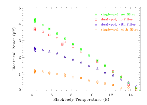
The blackbody illuminator in the optical efficiency measurements is made of carbon loaded Stycast-2850 epoxy, temperature controlled between 4K and 20K. The of the prototype detectors are designed to be K. We measure the thermal conductance of the bolometers, usually denoted by , by fixing the blackbody temperature at 4K and varying the cold plate temperature. To derive the optical efficiency, we acquire TES curves as a function of the blackbody temperature while holding the cold plate temperature. At each blackbody temperature, several curves are obtained as consistency check. The electrical power required to maintain the TES at a fixed resistance (1/2 the transition) is calculated from each curve. The thermal conductance, measured to be around 0.5 nW/K, is used to correct for the cold plate temperature fluctuations during TES curve measurements. After the correction, the points form a straight line, with the slope indicating the optical coupling of the detector to the illuminator (Figure 6). The TES normal resistance and shunt resistance are independently measured at 4K with a 4-wire AC bridge, minimizing the errors introduced by parasitic series resistance (normally ).
These measurements provide normalization to the FTS spectra, however, it should be pointed out that the filtering in this test is significantly less than that in the FTS measurements. Therefore the FTS spectra do not exactly represent the transmittance in the optical efficiency measurements.
4 Integrating the array with a polarization receiver
4.1 Fabrication reliability and uniformity
The summing network consists of many long and thin microstrip transmission lines, each of which crosses 2 steps in the ground plane created by the slot antenna. The prototype detectors described in §3 are fabricated with contact lithography. Already, judging from the measured angular responses, only one detector shows significant signs of failure in part of the summing network. The future arrays will be fabricated with stepper lithography, vastly improving the reliability and resolution of the structures. In addition, we have implemented a biased sputtered SiO2 process. By applying a DC voltage bias of several hundred volts during sputtering, the SiO2 layer exhibits a tapered edge profile, with better metal coverage and smoother, low impurity dielectric content. To demonstrate the reliability of the step coverage, we have fabricated a test device in which a 5m-wide meandering Nb microstrip is shown to have no breaks or shorts over its entire length of 255 mm and 3,800 cross-overs. We believe this level of reliability is adequate for the production of high yield antenna-coupled TES arrays.
To reduce wiring complexity, several TES in an array will share a common bias111In the current design, 32 TES using the same MUX chip will share a common bias.. It is therefore important to control the transition temperature, the normal resistance, and the thermal conductance of each TES. In the strong voltage bias limit (when the shunt resistance is much less than the TES resistance), the electrothermal equation reads
| (1) |
where is the optical power, , are the bath temperature and the transition temperature, and the bias voltage. defines the temperature dependent thermal conductance of the bolometer. A voltage-biased TES is self-biasing, in a sense that for a fixed bias voltage the resistance can vary freely from the normal resistance to zero to compensate for different loading . In practice, however, it is not desirable to operate the TES at a resistance below because of excess noise. It is apparent from this equation that variations in , , and across an array degrade the dynamic range of . For millimeter/far infrared instruments, the dynamic range in is usually designed to be a factor of a few. Moderate variations (up to 10 or 15%) in and cause only minor degradation in this factor. However, since is usually in the range of for silicon nitride at sub-K temperature, effects from variations are the most important.
The TES in the pathfinder array for balloon-borne SPIDER[20] will be based on elemental titanium. It is known that the of Ti films is close to the bulk value ( 0.42 K) and is fairly immune to thickness variations. To produce Mo/Cu or Mo/Au bi-layers with highly controlled poses a greater fabrication challenge. A dual- TES (0.42 K and 1.2 K) made from Ti and Al films is also under study. Such TES can will greatly help laboratory testing under high optical loading.
4.2 Polarization modulation/optics
Polarization modulators are often incorporated to aid the detection of a weak signal on top of a large unpolarized background. The types of polarization modulators include switches on the focal plane and external polarization modulators. The focal plane modulators include PIN diodes in correlation polarimeters[21], Faraday rotation modulators[22], MEM stripline switches[12], and superconductor-insulator-superconductor (SIS) inductance switches222We have successfully demonstrated an SIS switch that provides 80% modulation over a frequency range of 10%.. The most important example of an external modulator is a half-wave plate [23, 20].
To compare these different approaches, we recall the two primary purposes of modulators. First, they can put the signal frequency above the 1/f noise frequency. For correlation polarimeters [21], a fast modulator is essential to avoid gain fluctuations in the amplifiers. Bolometers are intrinsically very stable detectors. 1/f noise lower than 0.1 Hz is routinely achieved in various bolometric CMB experiments. Therefore, the performance in the second function of a polarization modulator, i.e., its ability to reduce polarization artifacts from the instrument, most notably the beam mismatch, passband mismatch, and gain mismatch [1, 24], is what should be weighted more in evaluating different modulation schemes.
Measuring polarization with bolometers generally requires taking differences of measurements at different polarization angles. Many effects associated with the beam, such as differential ellipticity and differential pointing, can create an artificial polarization signal. For a B-mode detection at T/S=0.01, the requirements for beams are very stringent [24]. However, if the polarization differences can be made with the same beam, these problems can be avoided. This idealized polarization rotation is most closely approximated by a rotating half-wave plate at the pupil of the optics. This is because that a half-wave plate locally rotates the direction of polarization without altering the field distribution, or the illumination. Other methods of polarization rotation, including sky/instrument rotation and all the on-chip modulators, do not help mitigate, and sometimes can even exacerbate the beam mismatch. For a detailed account of the systematic effects associated with polarization measurements and how a half wave plate help mitigate them, see the SPIDER paper in these Proceedings [20].
On-focal plane modulators do help alleviate 1/f fluctuations, and effects associated with focal plane temperature fluctuations and other scan-synchronous pick-ups. Given their advantages in speed, weight, and mechanical and cryogenic simplicity, on-focal plane modulators are still very worth pursuing alongside with the half-wave plates. For the first generation antenna-coupled TES, however, we assume that a rotating half-wave plate at the pupil is the primary mode of modulation. With the half-wave plate, the requirements for the beam are much more relaxed. The beams should be symmetric enough to produce a window function that is isotropic in space, and low in sidelobe content to avoid astronomical foregrounds. The beams produced by antenna-coupled bolometers (Figure 4) have already met these requirements.
5 Future plans
The current antenna-coupled TES prototype devices provide the first successful demonstration of this promising technology. We will continue to refine the microwave designs, with help from rapid feedback of optical characterizations. The wide bandwidth and well-understood impedance properties of long slot single polarization antenna can be used to study various downstream components, such as the summing network and filters. We have designed a new dual polarization architecture with a much larger bandwidth than that of the current design. The new antenna will be implemented in the next generation test detectors. Our current lumped-element filter design offers very good results in terms of in-band transmittance and out-of-band rejection. The absolute frequency control should improve with better fabrication techniques and experience.
Magnetic field shielding is an important issue for TES array and SQUID readout. We are currently setting up a SQUID multiplexing system for an adiabatic demagnetization refrigerator (ADR) system to test different magnetic field shielding schemes. In particular, we have the option of individually shielding each SQUID MUX chip with a superconducting enclosure. It is also necessary to shield the strong fields from the ADR. From our experience, an attenuation of 60-80 dB can be achieved with a few layers of high permeability cryoperm shield, Metglas sheets, and niobium foils. Tests carried out in an ADR system in NIST suggest that adequate magnetic shielding is fairly straightforward to achieve. More detailed characterization of the noise needs to be done to answer these questions further.
These detectors will first be used in the upgrade of the Robinson gravitational wave telescope[25], and SPIDER, a proposed balloon-borne experiment [20]. Robinson II and SPIDER share common design concepts, including large throughput cold refractive telescope that produces extremely low cross-polarization, instrument polarization, instrument loading, and beam ellipticity. The 30 cm compact optics enables detailed pre-flight characterizations, and provides an angular resolution of suitable for primordial B-mode polarization.
Despite these similarities, the two experiments are based on very different observing strategies. SPIDER is targeting very large angular scale CMB polarization, including the re-ionization bump at . It will survey 50% of the sky. To facilitate Galactic foreground removal on large angular scales, SPIDER payload consists of 6 monochromatic telescopes, covering a wide frequency range of 80-275 GHz with 2312 antenna-coupled TES bolometers. Multiple telescopes enable each to be monochromatic, thereby improving the performance of AR coatings, enabling a simplified wave plate design, and providing a large system throughput with minimum aperture size. On the other hand, Robinson II will be observing from South Pole through the 100 GHz and 150 GHz atmospheric windows. With the long integration time available from the ground, it will go extremely deep on 1-2% of the sky that has minimum astronomical foregrounds.
Both experiments will be an important scientific pathfinder for CMBPol, a comprehensive NASA satellite to study the CMB polarization [1]. In addition, many technical aspects discussed in this paper will be thoroughly tested. We believe the antenna-coupled TES detector technology is a strong candidate for CMBPol.
Acknowledgements.
The authors acknowledge support from the JPL Research and Technology Development program for supporting the TES development and SQUID multiplexer testing, and a 2004 NASA/APRA grant ”Antenna-Coupled TES Bolometer Array for CMB Polarimetry” to J. Bock. CLK acknowledges the support of a NASA postdoctoral fellowship.References
- [1] J. Bock, S. Church, M. Devlin, G. Hinshaw, A. Lange, A. Lee, L. Page, B. Partridge, J. Ruhl, M. Tegmark, P. Timbie, R. Weiss, B. Winstein, and M. Zaldarriaga, “Task Force on Cosmic Microwave Background Research,” ArXiv Astrophysics e-prints astro-ph/0604101, Apr. 2006.
- [2] J. J. Bock, D. Chen, P. D. Mauskopf, and A. E. Lange, “A Novel Bolometer for Infrared and Millimeter-Wave Astrophysics,” Space Science Reviews 74, pp. 229–235, Nov. 1995.
- [3] A. D. Turner et al., “Silicon nitride Micromesh Bolometer Array for Submillimeter Astrophysics,” Applied Optics 40, pp. 4921–4932, Oct. 2001.
- [4] W. C. Jones, R. Bhatia, J. J. Bock, and A. E. Lange, “A Polarization Sensitive Bolometric Receiver for Observations of the Cosmic Microwave Background,” in Millimeter and Submillimeter Detectors for Astronomy. Proceedings of the SPIE, Volume 4855, T. G. Phillips and J. Zmuidzinas, eds., pp. 227–238, Feb. 2003.
- [5] P. A. J. de Korte et al., “Time-division superconducting quantum interference device multiplexer for transition-edge sensors,” Review of Scientific Instruments 74, pp. 3807–3815, Aug. 2003.
- [6] T. M. Lanting et al., “Frequency-domain multiplexed readout of transition-edge sensor arrays with a superconducting quantum interference device,” Applied Physics Letters 86, pp. 2511–+, Mar. 2005.
- [7] M. J. Griffin, J. J. Bock, and W. K. Gear, “Relative performance of filled and feedhorn-coupled focal-plane architectures,” Applied Optics 41, pp. 6543–6554, Nov. 2002.
- [8] S. R. Dicker et al., “A 90-GHz array for use on the Green Bank Telescope,” in Proceedings of the SPIE, Volume 5489., J. M. Oschmann, ed., pp. 1221–1229, Oct. 2004.
- [9] A. Goldin et al., “Design of broadband filters and antennas for SAMBA,” in Millimeter and Submillimeter Detectors for Astronomy. Proceedings of the SPIE, Volume 4855., T. G. Phillips and J. Zmuidzinas, eds., pp. 163–171, Feb. 2003.
- [10] A. Goldin et al., “Antennas for bolometric focal plane,” Nuclear Instruments and Methods in Physics Research A 520, pp. 390–392, Mar. 2004.
- [11] M. J. Myers et al., “An antenna-coupled bolometer with an integrated microstrip bandpass filter,” Applied Physics Letters 86, pp. 4103–+, Mar. 2005.
- [12] D. Chuss et al., “The Primordial Anisotropy Polarization Pathfinder Array (PAPPA): Instrument Overview And Status,” in Proceedings of the SPIE, 2006.
- [13] J. Ward, F. Rice, G. Chattopadhyay, and J. Zmuidzinas, “SuperMix: A Flexible Software Library for High-Frequency Circuit Simulation, Including SIS Mixers and Superconducting Elements,” in Proceedings of Tenth International Symposium on Space Terahertz Technology, pp. 268–281, 1999.
- [14] K. D. Irwin, “An application of electrothermal feedback for high resolution cryogenic particle detection,” Applied Physics Letters 66, pp. 1998–2000, Apr. 1995.
- [15] P. D. Mauskopf et al., “Composite infrared bolometers with Si 3 N 4 micromesh absorbers,” Applied Optics 36, pp. 765–771, Feb. 1997.
- [16] S. Ali et al., “Antenna-coupled transition-edge hot-electron microbolometers,” in Proceedings of the SPIE, Volume 5498., J. Zmuidzinas, W. S. Holland, and S. Withington, eds., pp. 381–389, Oct. 2004.
- [17] B. S. Karasik, W. R. McGrath, M. E. Gershenson, and A. V. Sergeev, “Photon-noise-limited direct detector based on disorder-controlled electron heating,” Journal of Applied Physics 87, pp. 7586–7588, May 2000.
- [18] M. Kenyon et al., “Background-limited membrane-isolated TES bolometers for far-IR/submillimeter direct-detection spectroscopy,” in the 11th International Workshop on Low Temperature Detectors, 2005.
- [19] K. D. Irwin and K. W. Lehnert, “Microwave SQUID multiplexer,” Applied Physics Letters 85, pp. 2107–+, Sept. 2004.
- [20] T. Montroy et al., “SPIDER: a New Balloon-Borne Experiment to Measure CMB Polarization on Large Angular Scales,” in Proceedings of the SPIE, 2006.
- [21] D. Barkats et al., “Cosmic Microwave Background Polarimetry Using Correlation Receivers with the PIQUE and CAPMAP Experiments,” Astrophysical Journal Supp. 159, pp. 1–26, July 2005.
- [22] B. G. Keating, P. A. R. Ade, J. J. Bock, E. Hivon, W. L. Holzapfel, A. E. Lange, H. Nguyen, and K. W. Yoon, “BICEP: a large angular scale CMB polarimeter,” in Polarimetry in Astronomy. Edited by Silvano Fineschi . Proceedings of the SPIE, Volume 4843., S. Fineschi, ed., pp. 284–295, Feb. 2003.
- [23] P. Oxley et al., “The EBEX experiment,” in Proceedings of the SPIE, Volume 5543., M. Strojnik, ed., pp. 320–331, Nov. 2004.
- [24] W. Hu, M. M. Hedman, and M. Zaldarriaga, “Benchmark parameters for CMB polarization experiments,” Physical Review D 67, pp. 043004–+, Feb. 2003.
- [25] K. Yoon et al., “The Robinson Gravitational Wave Background Telescope,” in Proceedings of the SPIE, 2006.