Evaluation of 5 mm-thick CdTe Detectors from the Company Acrorad
Abstract
Using 220.5 cm3 Cadmium Telluride (CdTe) substrates from the company Acrorad, we have fabricated detectors with planar cathode contacts and 88 anode pixels. We investigate the I-V characteristics and energy resolution of the detectors for different contact materials and surface treatments. After biasing the detectors for a certain time, the dark currents increase dramatically. Our studies show that the time before breakdown decreases for higher detector temperatures and for higher applied bias voltages. We obtained the best results with a Pt cathode contact and In anode pixels when we heat the detector to 90∘C for 30 minutes prior to depositing the In contacts. Flood-illuminating the detector with 662 keV X-rays, we measured the pulse length distribution and derived an electron mobility of 860 cm2 V-1 s-1. We show that the energy resolution can be improved by correcting the anode signals for the depth of the primary interaction. Operated at a temperature of -40∘C and a cathode bias voltage of -500 V, the best pixels of the best detector achieved full width half maximum (FWHM) energy resolutions of 8 keV (6.4%) and 23 keV (3.4%) at 122 keV and 662 keV, respectively.
Index Terms:
CdTe, CdTe detectors, contacting technologyI Introduction
Cadmium Telluride (CdTe) and Cadmium Zinc Telluride (CZT) detectors are having a major impact on the field of hard X-ray astronomy. The Swift[1] satellite carries the Burst Alert Telescope (BAT) that uses CZT detectors. The International Gamma-Ray Astrophysics Laboratory (INTEGRAL)[2] includes the Imager on Board the Integral Satellite (IBIS) which is built with CdTe detectors. NASA’s Beyond Einstein roadmap included two X-ray missions, Constellation-X[3] and the Black Hole Finder Probe (BHFP). CZT detectors will play an important role for both missions. The Energetic X-ray Imaging Survey Telescope (EXIST)[4] is a strong candidate for the BHFP and uses pixelated Si and 0.5 cm thick CZT detectors and the coded mask approach to cover the energy range from 5 keV to 600 keV. The Non-thermal Energy eXploration Telescope (NeXT)[5][6] mission proposed in Japan is a successor to the Suzaku mission and will utilize CdTe on two of its instruments. The Hard X-ray Imager (HXI) on board NeXT will cover the energy range from 8 to 80 keV using a Si CCD combined with a pixelated CdTe detector. NeXT will also carry the Soft-Gamma Detector (SGD), which uses CdTe for an extended energy range up to 1 MeV. The broad energy ranges of these missions requires either thick detectors or layers of thin detectors. In this presentation, we focus on 5 mm-thick CdTe detectors.
While CdTe detectors show at room temperature a poorer performance than CZT detectors, CdTe might be an alternative to CZT in spaceborne applications where temperatures around -20∘C can be achieved without the need for cryogenic cooling. Several groups tested relatively thin CdTe detectors (e.g. [7, 8, 9, 10]). We report here on results from evaluating 0.5 cm thick CdTe detectors. Using substrates from the company Acrorad [11], we deposited different cathode and anode contacts and measured the I-V characteristics, the energy resolutions, and the electron mobility.
II Detector Fabrication
We purchased two uncontacted 220.5 cm3 CdTe substrates from Acrorad. In the following, we refer to the two detectors as D1 and D2. The substrates were cleaned in DI water and methanol. Prior to contact deposition, the detectors were polished with three grades of abrasive paper followed by 0.3 and 0.05 m alumina suspension. Optionally, the detectors were etched for 2 minutes in a solution of 5% Br in 95% methanol. We deposited planar cathode contacts and anode pixels on the CdTe substrates with an electron beam evaporator. The 1.6 mm diameter pixels with 2.4 mm pixel pitch were deposited using a 0.3 mm brass foil shadow mask. The first detectors showed modest performances. We thus started to use a method similar to the one described by Takahashi et al. (1999), and heated D1 at 90∘C (30 minutes) and D2 at 140∘C (15 minutes) prior to the deposition of the anode contacts. The heating was performed in a 10-7 Torr vacuum with the anode side facing an Hg lamp, and a temperature sensor being attached to the backside of the detector. As discussed further below, the heat treatment markedly improved the energy resolution achieved with the detectors.
We used the high-workfunction metals Au and Pt as cathode materials and the low-workfunction metal In as anode material. The high-workfunction Au and Pt metals are expected to form ohmic contacts on the p-type CdTe and the low-workfunction contacts blocking contacts. The heat treatment is thought to remove the Te-rich surface layer and to improve the contact properties of the CdTe–In junctions [7]. We will refer to the two detectors as D1a-D1b and D2a-D2c, depending on which surface treatments and contact materials were used (see Table 1).
III Results
III-A I-V Characteristics
We measured the pixel-cathode dark current as a function of the cathode bias voltage for detector temperatures between C and 20∘C. Holding all pixels at ground potential, the currents were measured for three central pixels.
After keeping the detectors biased at a certain voltage for some time, we observed the well known breakdown phenomenon: a dramatic increase of the dark current. We found that if the bias voltage was set to zero after a breakdown and then immediately returned to its previous value, the breakdown would occur after a shorter period of time. However, if the bias voltage remained at zero for several minutes and was then returned to its previous value, the breakdown time would be very similar to its original value.
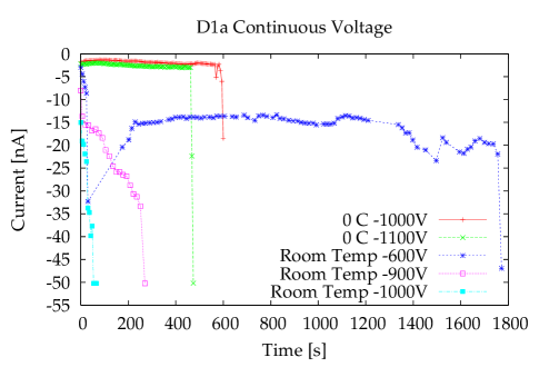
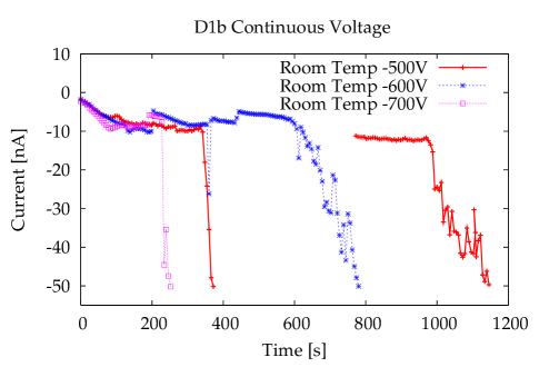
Figure 1 shows the current for the detector D1a at different temperatures and different bias voltages. It is evident that the time before breakdown decreases with increasing detector temperature and with more negative cathode bias voltages. Figure 2 shows a very similar breakdown behaviour for the same crystal, this time depositing the In pixels after polishing, etching, and heat treatment (detector D1b). As discussed further below, our heat treatment may have used temperatures too low to strongly suppress the breakdown behaviour.
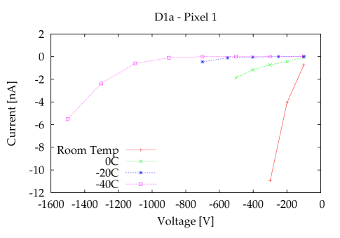
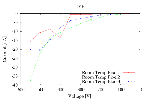
The I-V measurements showed a wide range of variation from detector to detector and from pixel to pixel. Figure 3 shows the dark current for the detector D1a as a function of bias voltage for various temperatures. All measurements were taken before breakdown occurred. It can be recognized that the I-V characteristics are non-linear. Figure 4 shows the measurements for three pixels on D1b; a large variation from pixel to pixel can be recognized. Figure 5 compares the results for D2a (Pt cathode) and D2b (Au cathode). The detector with Au cathode shows very high dark currents that compromise the detector’s spectroscopic performance.

III-B Energy Resolution and Mobility Measurements
The energy resolutions of the detectors were determined using a 662 keV X-ray source and cooling the detectors to C. The same three pixels for which the I-V measurements were performed were also used for measuring the energy spectra. A cathode bias voltage of -500 V was applied; at C this voltage allowed us to operate the detectors without incurring breakdown. The pixels were held at ground and AC coupled to a fast Amptek 250 amplifier followed by a second-stage amplifier. The signals were sampled with a 500 MHz oscilloscope and the digitized pulses were send to a computer via Ethernet. High-frequency filtering was done offline. The amplifier noise was 5 keV at -40∘C and was subtracted in quadrature from the measured resolutions. In most cases, the amplifier noise was negligible compared to the inherent detector resolution. A more detailed description of the measurement setup can be found in Krawczynski et al. (2005)
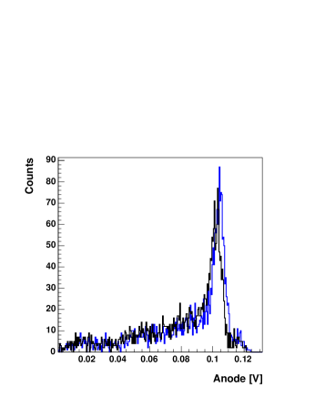
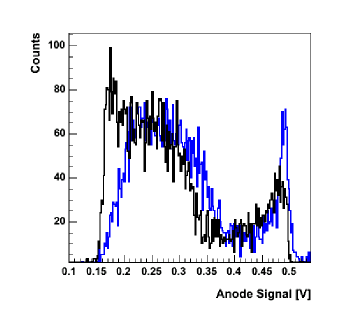
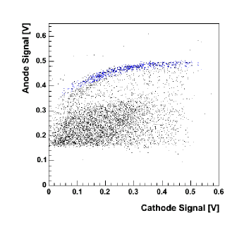
Owing to trapping of electrons and poor hole mobility, interactions occurring near the cathode produce larger anode signals than those that occur near the anodes. This depth of interaction (DOI) effect can be corrected by comparing the anode and cathode signals for each pulse. Figure 6 shows the anode vs. cathode pulse heights. Photopeak events are highlighted in blue. The original and corrected 122 keV and 662 keV energy spectra for a detector D1b pixel are displayed in Figs. 7 and 8. After correction we obtain 122 keV and 662 keV full width half maximum (FWHM) energy resolutions of 8 keV (6.4%) and 23 keV (3.4%), respectively.
| Detector | Cathode/ | Surface | Energy |
| Anode | Treatmenta | Resolution | |
| (662 keV) | |||
| D1a | Pt/In | Polish | 8.4% |
| D1b | Pt/In | Polish, Etch(2 min), | 3.4% |
| Heat (90∘C-30 min) | |||
| D2c | Pt/In | Polish | High Leakage |
| Current | |||
| D2a | Au/In | Polish | High Leakage |
| Current | |||
| D2b | Pt/In | Polish, Etch(2 min), | 8.3% |
| Heat (140∘C,15 min) |
a The etching and heat treatment were performed only prior to depositing the In anodes. The cathodes were always deposited on the surfaces as polished.
The energy resolution does depend on the surface treatment and the choice of contact materials. Table 1 gives the 662 keV resolutions for the different combinations of substrate, surface treatment, and contact material. Energy resolutions varied widely from detector to detector and from pixel to pixel. Here only the results for the best pixels are reported. For all the detectors, we tested three central pixels. The energy resolutions differed from pixel to pixel by 25%. It is evident that the combination of etching and heat treatment prior to contact deposition improves the performance for both detectors. While the detector D2 did not produce a spectrum with any photopeak prior to etching and heating, it did show a photopeak afterward, although the 662 keV energy resolution (55 keV, 8.3%) was still very modest. For the detector D1, the 662 keV energy resolution improved from 56 keV (8.4%) before heating and etching to 23 keV (3.4%) after etching and heating.
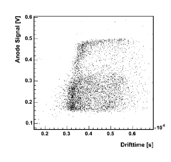
Our test-setup allows us to measure the rise time of the pulses and thus to measure the electron drift times. Assuming that the detector is fully depleted, the longest pulse times result from electrons travelling the full 0.5 cm thickness of the detector, and the electron mobility can be computed. Figure 9 shows the drift times for detector D1b. Longest drift times of translate into a -value of cm2 V-1 s-1.
IV Conclusion
We have presented here results on the spectroscopic performance of 0.5 cm thick CdTe crystals from the company Acrorad with a variety of electrodes fabricated by Washington Univeristy in St. Louis. At a substrate temperature of -40∘C, our best results are 122 keV and 662 keV resolutions of 8 keV (6.4%) and 23 keV (3.4%), respectively. We have shown that changes in the surface preparation yield widely different detector performances. Our detectors showed a breakdown if biased for a sufficient time; the time before breakdown was longer for lower bias voltages and at colder detector temperatures. We cannot exclude the possibility that a combination of low bias voltage and low temperature may suppress the breakdown completely.
Other authors have experimented with between 0.5 and 2.0 mm thick CdTe detectors. For example, using a 0.5 mm thick detector with an area of 1.91.9 cm2, Oonuki et al. (2005) report 122 keV and 511 keV energy resolutions of 1.6 keV (1.3%) and 5.0 keV (1%). Comparison of these results with our results is difficult as Oonuki et al optimized the contact deposition procedure with very detailed studies. We thus cannot determine to which degree the difference in detector performance results from the different detector thicknesses and from the different contacting techniques.
Acknowledgment
This work was supported by NASA under contract NNG04WC176. We thank T. Takahashi for very useful discussions.
References
- [1] Gehrels, N. Proc. SPIE 4140, 42, 2000.
- [2] Ubertine, P. et al. A&A 411 L131, 2003.
- [3] The Constellation Project Team, Constellation-X Technology Readiness and Implementation Plan (TRIP) Report. http://constellation.gsfc.nasa.gov/images/science/resources/documents/ TRIPReport_NoCost.pdf
- [4] Grindlay, J.E. et al. Proc. SPIE 4851, 331, 2003.
- [5] NeXT Satellite Proposal, the NeXT working group, ISAS, 2003, submitted for publication.
- [6] Kunieda, H., Proc. SPIE 5488 (2004) 187
- [7] Takahashi, T. et al. NIMA 436 111, 1999.
- [8] Oonuki, K., Tanaka, T., Watanabe, S., et al. Proc. SPIE 5922 (2005) 59220J-1
- [9] Gnatyuk, V., Aoki, T., Hatanaka, Y., et al. Proc. SPIE 5922 (2005) 59220I-1
- [10] Aoki, T., Ishida, Y., Morii, H., et al. Proc. SPIE 5922 (2005) 59220T-1
- [11] Acrorad Co., Ltd., Wataru. Inui, 1-27-16, Hamamatsucho, Minatoku, Tokyo 105-0013
- [12] Krawczynski, H., Jung, I.V., Perkins, J., Burger, A., Groza, M. SPIE 49, 5540, 13.01.(2004).