Near room temperature X-ray and -ray spectroscopic detectors for future space experiments
Abstract
New generation Cadmium Telluride (CZT & CdTe) solid state detectors can provide high quantum efficiency with reasonably good energy resolution and can operate at near room temperature; an unique advantage for space experiments. We present here results of our study of small diode detectors as well as large area pixel detectors. Our study is aimed at developing near room temperature hard X-ray spectroscopy detectors for ASTROSAT and other future Indian space science missions. We have studied a Si-PIN detector in the energy range 5 - 60 keV and CZT & CdTe Schottky diode detectors in the energy region 10 - 1330 keV. Our results suggest that the energy resolution is limited by the thermal/electronic noise in the low energy region ( 60 keV) while it is affected by the charge transport properties of the detector in the higher energy region ( 100 keV). We have studied large area (64 cm2) CZT pixel detectors with pixel size close to the small CZT detector. We have studied individual pixels as well as CZT detector as a whole (summed over all the 1024 pixels). The CZT pixel detectors are single carrier detectors with peaking time 1 s. The energy resolution behaviour of the large area CZT detector is similar to that of small diode detectors in the low energy region. The change in operating temperature from room temperature 20oC to 70oC drastically affects both the energy resolution as well as the peak area due to a sharp rise in the thermal noise. These results suggest that the cooling of detector system will provide better energy resolution as well as detection efficiency. Our results also show that the crystal uniformity is another important issue in the case of large area CZT pixel detectors.
keywords:
CdTe; CZT; Diode detectors; Pixel arrayPACS:
29.40.Wk1 Introduction
Table 1: Properties of the semiconductor detectors
| Semiconductor | density | Z | Egap | X0 | Eintrinsic | |
|---|---|---|---|---|---|---|
| (g/cm3) | (eV) | (eV) | (mm) | eV@100 keV | ||
| Si | 2.33 | 14 | 1.12 | 3.6 | 25 | 446 |
| Ge | 5.33 | 32 | 0.67 | 2.9 | 3.3 | 400 |
| CdTe | 5.85 | 48, 52 | 1.44 | 4.43 | 1 | 495 |
| CZT | 5.81 | 48, 30, 52 | 1.6 | 4.6 | 1 | 504 |
Egap : band gap energy, : ionization potential, X0 : radiation length
In hard X-ray spectroscopy (for astronomy or planetary mapping), the basic requirement is high sensitivity with high energy resolution which can detect weak closely spaced lines above the background. The best energy resolution among the diode detectors is obtained using Ge diode detectors (E/E 500), if they are cryogenically cooled to reduce the leakage current and thermal noise. In space experiments, the detector requirements are high detection efficiency, high energy resolution and operating temperature close to room temperature (does not need expensive and cumbersome cryogenic cooling). The ideal detector for space experiments should have high atomic number, high density and a band gap much larger than that of Ge which can allow operating temperature close to room temperature (Table 1 lists some of the properties of the semiconductor detectors). In the last column, we give the intrinsic energy resolution calculated from statistical fluctuations in the number of electron-hole pairs created in photon interaction and assuming the fano factor f=0.1 for all the detectors [4,5]. Cadmium Telluride Cd1-xZnxTe (CdTe and CZT) has been regarded as promising material for hard X-ray studies. Its high atomic number gives a high quantum efficiency and a large band gap allows these detectors to operate at near room temperature. However the high defect density in these detectors results in considerable charge trapping. This leads to charge transport properties far inferior to those of Si and Ge detectors. The high defect density is also the main source of leakage current in these detectors.
Till recently, CZT was the best hard X-ray spectroscopy detector operating at near room temperature as it has lower leakage current than the CdTe detectors. The charge transport properties were the limitation of CZT detectors: for electron 1-210 and for hole 110, where is the mobility and is the life time of the charge carriers [6]. This severely limits the effective depth of CZT detectors and hence the energy range. The effective depth of 2 mm thick CZT detectors (investigated here) is commonly in the range of 0.5 to 1 mm. The CdTe detectors show superior charge transport properties: for electron 1-210 and for hole 210. The hole lifetime in CdTe is typically 2 sec, more than an order of magnitude larger than in CZT. Thus, a 1 mm thick CdTe detector (investigated here) will have effective depth close to its physical depth. Recently developed CdTe Schottky diode detectors show further reduction in leakage current which permits the use of a much higher bias voltage, improving further the transport properties and the effective depth. The trapping lengths ( E where E is the electric field) for electrons and holes in CZT are 2.7 cm and 0.01 cm respectively while these values in CdTe are 13.2 cm and 0.8 cm for electrons and holes respectively (for E=400V).
2 Experimental details
Table 2: Some details of the diode detectors
| Detector type | CdTe Schottky diode | CZT | Si PIN diode |
| Detector size | 3x3 mm | 3x3 mm | 13 mm2 |
| Detector thickness | 1 mm | 2 mm | 300 m |
| Detector window | Be 250 m | Be 250 m | Be 25 m |
| Detector power[1] | 400V @ 1 A | 400V @ 1 A | 100V @ 1A |
| Preamp. sensitivity | 0.82 mV/keV | 0.73 mV/keV | 1 mV/keV |
Main details of the diode detector systems which we have studied in this paper are given in Table 2. All the detectors are from AMPTEK INC., USA. Specific power supply provides the main amplifier and the DC high voltage needed to operate each detector system. The thin Si-PIN diode detector (300 m thick) is intended to study soft X-rays below 30 keV while thick CZT and CdTe detectors are intended to study hard X-rays. The signal from the amplifier/power supply can be connected directly to a MCA (multichannel analyzer) or an oscilloscope. We have used pocket MCAs (model 166 from GBS and MCA 8000A from AMPTEK) connected to a PC or laptop for acquiring and storing the spectra. All the detectors are cooled using thermoelectric cooler to C along with input FET transistor, A250 charge sensitive preamplifier and the current feedback network [1]. A temperature monitoring integrated circuit is placed on the cooled substrate to provide a direct reading of the temperature of the internal components.
The cooling of the detector reduces the leakage current considerably, thus permitting the high positive bias voltage of 400V in case of CZT and CdTe detectors which further improves the charge transport properties. Recently developed CdTe Schottky diode detectors which are fabricated using blocking (Schottky) diodes rather than the symmetric contact on CdTe show large reduction in leakage current [7]. The charge transport properties in CdTe detector are much superior to those of CZT, still the charge loss is not negligible. The electron/hole pairs created in the detector near the back contact by radiation result in fluctuations in charge collection time. As a result, the acquired spectra suffer from increased background counts and degraded energy resolution. To reduce these effects, a rise time discrimination (RTD) circuit has been used in the power supply/amplifier with shaping time 3 s. When the RTD is ON, the shaped pulses are internally gated and only pulses corresponding to “full charge collection” events are allowed to be sent to the MCA. In all our observations, the RTD is kept ON.
We have also studied large area CZT pixel detectors from IDEAS, Norway and the details are given in section 4 along with the results.
3 Observations and Results
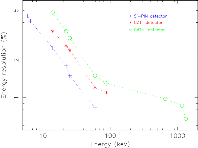
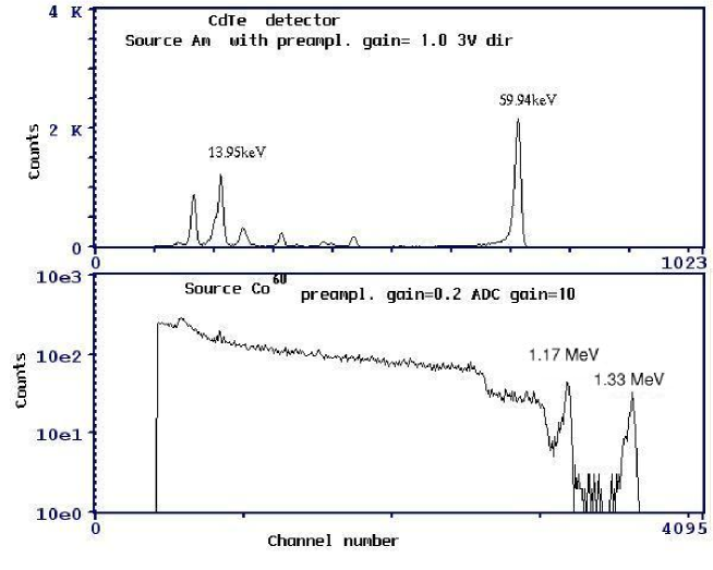
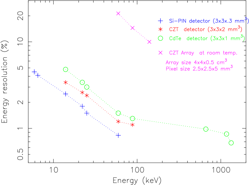
In Figure 1, we show Am241 spectrum in the top panel for 200 sec acquisition time and Co60 spectrum in the bottom panel for 30000 sec acquisition time using CdTe detector. All important energy lines are marked. These results demonstrate the high efficiency of the CdTe detector in a wide spectral range from 10 keV to 1330 keV with good energy resolution. Our results of measured energy resolution vs energy for CdTe, CZT and Si-PIN detectors are shown in Figure 2. The energy resolution is defined as the FWHM of a peak in % of the energy. The Si-PIN detector provides better energy resolution than CdTe and CZT detectors in low energy region. The quantum efficiency of Si-PIN limits its energy to 30 keV. We could also not detect the 662 keV line with the 2 mm thick CZT detector. These results suggest high hole trapping and poor charge collection in CZT at higher energies and much superior charge transport properties of CdTe detectors. This limits the energy range of the CZT detector to the range between 10 keV and a few hundred keV. However the CZT detector provides better energy resolution than the CdTe detector suggesting lower thermal/electronic noise. These results also suggest that a thicker CZT detector (as used in the CZT array) will not increase much the energy range but only affect adversely the energy resolution (see next section). We have also studied the effects of electronic noise, high radiation flux and detrapping by annealing. Results are discussed in a separate publication [13].
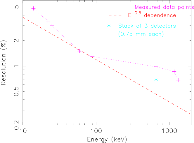
Figure 3 shows the measured energy resolution of the CdTe detector in the energy range 10-1330 keV (data points along the dotted line). The energy resolution is in the range 1-5 % below 88 keV and is around 1% in the wide energy range of 88 keV to 1330 keV. Due to the high atomic number, the photoelectric absorption is the main process up to 300 keV for CdTe as compared to 150 keV for Ge. The 1 mm thick CdTe has 64% detection efficiency at 100 keV which reduces to 4% at 1000 keV.
The background at 59.5 keV line in Am241 spectrum and at 88 keV line in Cd109 spectrum is negligible suggesting very little contribution from thermal/electronic noise. These energies are still low and interactions still occur close to the detector surface and one can reasonably assume that the effect of charge collection loss is negligible at these energies. We fit expected energy dependence of E-0.5 in this energy range (dashed line) and study the deviation of the measured energy resolution. The energy resolution is increasingly affected at lower energies by thermal/electronic noise below 60 keV while at higher energies ( 100 keV), the charge collection properties severely affect the energy resolution (operating temperature -30 oC). At 1330 keV the observed energy resolution is 0.68% while expected resolution is 0.2% (dashed line). For 662 keV line, measured energy resolution is 0.98% while expected energy resolution is 0.46%. A stack of three CdTe detectors with each of 0.75 mm thick (2.25 mm total thickness) provides 0.69% energy resolution at 662 keV (shown by star in the Figure 3, AMPTEK Web-page). A stack of thin CdTe detectors provides better charge collection properties and hence improves energy resolution. Thus a stack of thin CdTe detectors can cover a wide energy range at reasonably good energy resolution [8].
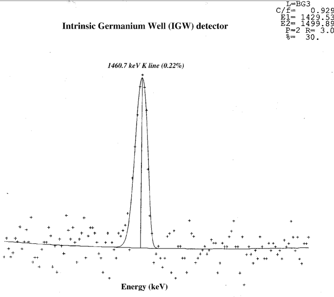
In X-ray spectroscopy or in planetary mapping, one would desire to detect weak lines above background which requires a high performance detector with very good energy resolution. It is known that the background continuum emitted from the moon surface has substantially larger flux than the sum of all the lines of interest. It may be noted here that a large size Ge detector is being used in Mars Odyssey mission for mapping of the Mars. In Figure 4, we show the energy spectrum of a neutron-activated sample in the range 1430 keV - 1500 keV as measured by a Ge detector cryogenically cooled to 77 K [2]. The spectrum exhibits a strong K line at 1460.7 keV with 0.22% energy resolution. This value is close to the expected energy resolution in CdTe detector as discussed before. We therefore conclude that the deterioration of energy resolution in thick CdTe is caused by bad charge transport properties of the detector material and a better energy resolution can be achieved by a stack of thin detectors.


4 Test with large CZT array
Initially the large area pixel detectors were planned as CZT detectors as this material provides by an order of magnitude lower leakage current [6]. The small pixel size is one way to reduce further the leakage current as well as it can provide imaging. Handling a large number (several thousands) of amplifiers and related front-end electronics is one of the critical R&D areas in the development of large area CZT detectors. Normally, this is achieved by designing Application Specific Integrated Circuits (ASIC). We have studied large area CZT array systems provided by Ideas, Norway (with XAIM3.2 ASIC readout) which use CZT crystals developed by IMARAD Imaging System, Israel. Each module uses 44 cm2 CZT crystal with 0.5 cm depth (crystals are grown using the modified Bridgeman method). The pixel size is 2.462.46 mm2. The total pixels are 256 per module (1616) and each module has its own ASICS (2 for each module) [9]. It uses Gold/Gold contacts and a floating guard band of the adhesive tape with a metallic strip deposited near one end [12]. It is known that the IMARAD CZT material is slightly N type and a negative bias of -600V is used. The default peaking time is 0.5 s. The leakage current is in the range of 10-30 nA. We can operate four such modules in our current system which has arrangement to cool the detectors during operation by a liquid coolant. The detector module is supposed to provide less than 10 % energy resolution at 140 keV with more than 40 % photo peak efficiency.
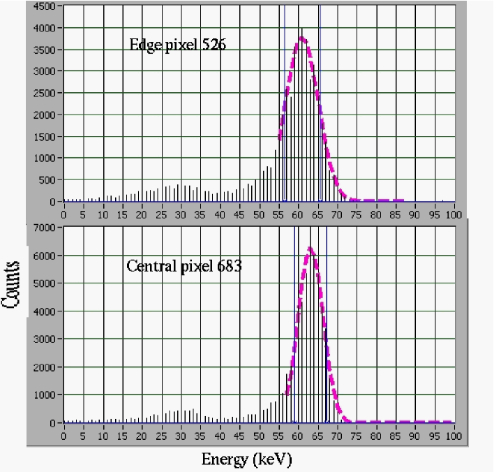
We show in Figure 5 the spectra of Co60 for 10 sec accumulation time from an edge pixel and a central pixel (pixel numbers 526 and 683 respectively) at 240C. The thick dotted lines show the Gaussian fits to high energy region of the peaks (excluding the tailing part at low energy). The central pixels usually provide better energy resolution than the edge pixels.
Each detector module/ASICS system consumes 0.82 W power. If cooling is not used, the dissipation of heat will raise the temperature of the system. In this work, we study the detector system without cooling. We have studied the effect of rising temperature on the energy resolution. The energy resolution is given as standard deviation (FWHM = 2.35 ) in % of peak position. We have used a thermal sensor to measure the temperature of detector/ASICS system. A special thermal grease is used for thermal contact between the thermal sensor and the cooling finger attached to the detector/ASICS system. The temperature rises from 24oC at the start and stabilizes at 32oC in about two hours time (here 32oC is a lower limit on the temperature of the detector system which may be higher due to the temperature gradient). We assume that the detector system is initially in equilibrium with room temperature and any quick measurements within 10-20 sec are assigned to the room temperature. For longer durations, the detector heats up and a temperature gradient appears. We will refer to it as “heated temperature”. Later in this section we will show that the actual temperature of the detector may be as high as 70oC when our thermal sensor attached to the cooling finger shows around 30oC. The result of heating is shown in Figure 6. The energy resolution degrades during the first two hours. Initially the change in energy resolution is faster for the central pixel (# 683) than for the edge pixel (# 526) as expected. This reveals a spatially inhomogeneous rise of thermal noise and background. The energy resolution degrades by about 4%. We have also studied the effect of rising temperature on the peak area. The peak area is calculated within assuming a Gaussian peak shape based on the measured and peak height. The results are shown in Figure 7. For both the pixels, edge and central, the change in the peak area coincides, suggesting a global effect. It is most likely the dead time/multi hit due to sharp rise in the thermal noise which will be clear as we discuss our results of background at different temperature in Figures 8 and 9.
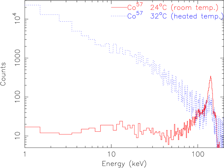
We show Co57 spectra for 10 sec accumulation time in Figure 8 taken at room temperature 24oC and at heated temperature 32oC after two hours of operation. Both the spectra are summed over all the 1024 pixels. The energy calibration is based on single energy of 60 keV (Am241). The 122 keV peak is clear in spectrum taken at room temperature 24oC while this peak is hardly distinguishable in spectrum taken at heated temperature 32oC. In two hours of operation, there is a sharp rise in the thermal noise/background counts in the low energy region. This is consistent with our explanations of Figures 6 & 7.
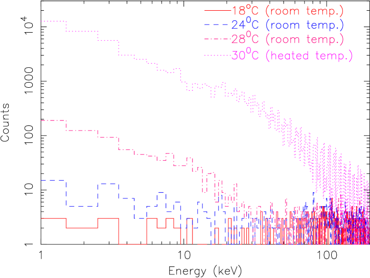
To prove further we study background spectra at different temperature. In Figure 9, we show the background spectra (summed over all the 1024 pixels) taken at room temperature 18oC, 24oC, 28oC and at heated temperature 30oC (after two hour operation). From the shape of the background spectrum at 18oC, it may be safely assumed that it is mostly of non-thermal origin with no significant contribution from thermal noise. The background spectrum taken at 28oC (room temp.) shows significant thermal noise contribution below 30 keV while at higher energies above 30 keV, the background spectrum is similar to one observed at 18oC (IDEAS has suggested operating temperature range 18-28oC for our detector system in the energy range 30-200 keV). The population of conduction electrons for a semiconductor at temperature T is given by
A is a constant (for the temperature range discussed here), Eg is band gap energy (1.6 eV) and k is Boltzmann constant. We have used background data at 28oC room temperature and at 30oC heated temperature (Figure 9). The rise in background is by a factor 50 in the energy range 1-10 keV. It gives the real temperature of the detector is 70oC after two hours of operation when our temperature sensor thermally attached to the cooling finger shows 30oC (the final equilibrium temperature after two hours of operation also depends on initial room temperature). These results show a raised temperature. A rise of 50oC (from room temperature 20oC to 70oC) affects both the energy resolution and the peak area. It is important to use ASICS with lower power or use cooling to keep background low when long duration operations are needed.

We have tested energy resolution of this system at room temperature. During the test at room temperature we have used four detector modules (64 cm2 area with 1024 pixels). The results are shown in Figure 10 along with results of small area diode detectors. The energy resolution behaviour of the large area CZT pixel detector is similar to the energy resolution behaviour of the small area diode detectors in the low energy ( 60 keV). The large area CZT pixel detector is likely to have same behaviour in the high energy region (above 100 keV) as (1) it uses fast peaking time of 0.5 s, and (2) the large area CZT pixel detectors are mostly single carrier detectors. At room temperature (24oC), the energy resolution of CZT array (summed over all pixels) is degraded by a factor of 18 compared to that of a small CZT detector, which is only 2 mm thick and was operated at -30oC. This factor rises to above 24 at 70oC (after two hours of operation). Even the best pixels exhibit a factor of 15 at 24oC. It is known that changing operating temperature from 20oC to -20oC results a drop in the leakage current by almost two order of magnitude [10]. Here, one can identify two main factors which are likely to degrade the energy resolution (1) the CZT array is being operated at room temperature while the small CZT detector is operated at -30o and, (2) the CZT array is thicker (5 mm thick) than the small CZT detector which would result more leakage current due to larger number of defect/trapping sites. Therefore, thiner CZT array would also be expected to improve the energy resolution. Both these factors will reduce the leakage current and hence improve the energy resolution. One needs to explore the low operating temperature range for CZT array detectors as there are reports that the IMARAD standard and Au detectors stop functioning around -20oC [11]. Recent results of the Schottky contact and the guard ring which show a drastic drop in leakage current (more than three order of magnitude) will bring further improvement in the energy resolution [8].
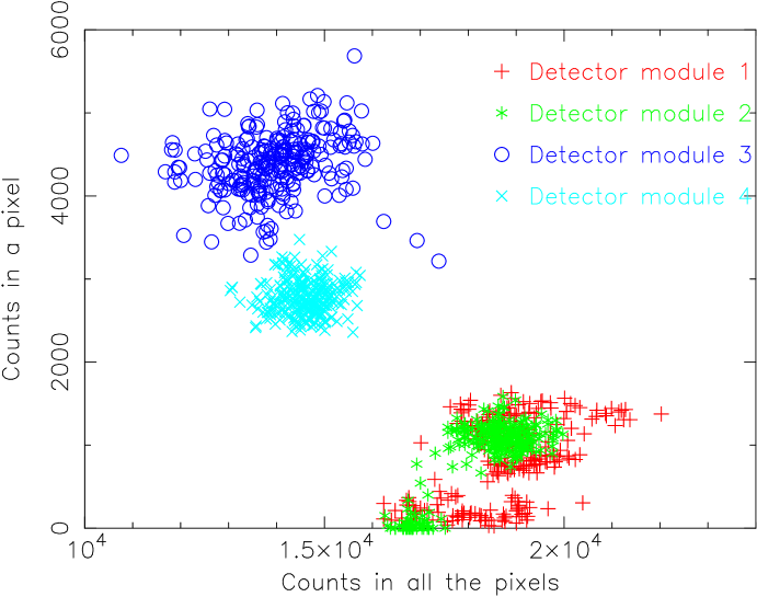
Another important issue with large area CZT pixel array detectors is the uniformity of the crystal. We have measured the energy resolution of individual pixels (central pixels, middle pixels and edge pixels) of the four CZT detector modules operating at 70oC (after 2 hours of operation) and results are shown in Figure 11. For central regions, is averaged over 10 pixels while it is averaged over 20 pixels for middle and outer pixels (bad pixels are excluded from this study). On an average, central pixels show better energy resolution than the edge pixels which is in agreement with previous studies [12]. The detector modules 2, 3 and 4 show typical variation in the energy resolution but detector module 1 shows large variation. Our further study of this detector module shows large patches of bad pixels which show bad detector properties suggesting non-uniform detector material. In Figure 12, the counts in individual pixel vs the counts summed over all the 1024 pixels are plotted for these four detector modules. A collimated Am241 source was used to irradiate each pixel. The beam size was less than the pixel size. This study includes all the pixels (including bad pixels). The detector modules 3 and 4 show good efficiency of individual pixels while detector modules 1 and 2 show that many pixels have poor performance with low detection efficiency (close to 0) in many cases. These results suggest cross talk between pixels as the counts summed over all the 1024 pixels increase. Both of these suggest bad crystal detection properties as well as non-uniformity of the detector material. It may be noted here that the energy resolution of individual pixel improves as the counts in the individual pixel increase (not shown).
5 Conclusions
New generation Cadmium Telluride Cd1-xZnxTe (CdTe and CZT) detectors provide great advantage of compactness and operating temperature close to room temperature for future space experiments due to their higher atomic number and higher band gap. The thermal/electronic noise affects the energy resolution in low energy while bad charge transport properties affect the energy resolution in higher energy range (100 keV). In case of large area CZT pixel detectors, the energy resolution behaviour is similar to that of the small diode detectors in the low energy region. In the space, low ambient temperature will reduce the problem of thermal/electronic noise. The large area CZT pixel detectors can provide good energy resolution as well as high quantum efficiency while operating at the ambient temperature in the space and hold bright prospect for future space experiments. It is capable of detecting most of the lines of interest in the case of moon -ray mapping [2]. For better energy resolution and better peak detection efficiency, a basic requirement in low count rate astronomy and planetary science, our results suggest the following: 1. use of low power ASICS, 2. decouple detector and ASICS (as most of the heat is produced in ASICS), and 3. use cooling to operate detector at low temperature. The INTEGRAL and SWIFT space missions are already using these new generation detectors to achieve their scientific goals [14,15]. Future developments in the crystal technology of compound semiconductors will reduce the gap in the energy resolution achieved with the cryogenically cooled Ge detector and CdTe detectors.
The Indian Multi-wavelength Satellite, ASTROSAT, has been planned with broad-band X-ray spectroscopy as one of its major objectives. One of its experiments is a large area (1024 cm2) CZT detector array. It will have a total of 16384 pixels and the pixel size will be 2.5 x 2.5 mm2 (5 mm depth) [3]. Recent progress in CdTe has shown superior charge transport properties and the effective depth close to its geometric depth. A stack of thin CdTe detectors can cover a wide energy range from 10 keV to a few MeV with reasonably good energy resolution. If we replace pixel material from CZT to CdTe, the same configuration will provide enormous advantage in the same energy range. These detectors will have very good efficiency close to 100% up to about 200 keV due to the superior charge transport properties of CdTe over CZT with similar or better energy resolution. Such a wide energy range (say 10 keV to 1 MeV; higher energy is limited by the detector size as well as the photon flux) will have enormous advantage in the study of non-thermal emission in astronomy.
Acknowledgments
We thank anonymous referee for constructive and very useful comments. We thank Prof. A. R. Rao and Prof. P. C. Agrawal for support and encouragement. We thank Mr. Parag Shah for technical help. We also thank Mrs S. Prabhudesai for help during these observations.
References
- [1] XR-100T-CdTe operating manual from AMPTEK Inc. Mass. 01730 USA (2003).
- [2] J. S. Yadav and J. R. Arnold, Nucl. Instr. & Meth., A195 (1990) 241.
- [3] A. R. Rao, Report on “Cadmium Zinc Telluride (CZT) Array for the ASTROSAT satellite (2002).
- [4] R. Gunnink and Rolf Arlt, Nucl. Instr. & Meth., A458 (2001) 196.
- [5] Glenn F. Knoll, Radiation detection and measurement, John Wiley and Sons, (1989) P.117.
- [6] T. Takahashi and S. Watanabe “Recent progress in CdTe and CdZnTe detectors, IEEE Trans. Nucl. Sci., 48,no. 3 (2001) 950.
- [7] O. Limousin, Nucl. Instr. & Meth., A504 (2003) 24.
- [8] T. Tanaka, Y. Kobayashi, T. Mitani et al., New Astronomy Rev. 48 (2004) 309.
- [9] A. R. Rao, J. S. Yadav, J. P. Malkar et al., Baseline Design Document (2004) 6.
- [10] K. Nakazawa, T. Takahashi, S. Watanabe et al., Nucl. Instr. & Meth., A512 (2003) 412.
- [11] T. Narita, P. F. Bloser, J. E. Grindlay et al., Astroph:0008275 (2000).
- [12] S. V. Vadawale, J. Hong, J. Grindlay et al., Astroph:0409085 (2004).
- [13] J. S. Yadav, S. Savitri, J. P. Malkar and S. Prabhudesai, TIFR Preprint, (2004).
- [14] F. Lebrun, J. P. Leray, P. Lavocat et al., A & A, 411(2003) L148.
- [15] N. Gehrels, New Astronomy Review 48 (2004) 431.