A Prototype Si/CdTe Compton Camera and the Polarization Measurement
Abstract
A Compton camera is the most promising approach for gamma-ray detection in the energy region from several hundred keV to MeV, especially for application in high energy astrophysics. In order to obtain good angular resolution, semiconductor detectors such as silicon, germanium and cadmium telluride(CdTe) have several advantages over scintillation detectors, which have been used so far. Based on the recent advances of high resolution CdTe and silicon imaging detectors, we are working on a Si/CdTe Compton camera. We have developed 64-pixel CdTe detectors with a pixel size of 2 mm2 mm and double-sided Si strip detectors(DSSDs) with a position resolution of 800m. As a prototype Si/CdTe Compton camera, we use a DSSD as a scatterer and two CdTe pixel detectors as an absorber. In order to verify its performance, we irradiate the camera with 100% linearly polarised 170 keV -rays and demonstrate the system works properly as a Compton camera. The resolution of the reconstructed scattering angle is 22∘(FWHM). Measurement of polarization is also reported. The polarimetric modulation factor is obtained to be 43%, which is consistent with the prediction of Monte Carlo simulations.
Index Terms:
Compton Camera, Semiconductor Detectors, CdTe, polarimeter.I Introduction
As gamma-ray energies increase to the MeV region, the detection of photons, the determination of the incident direction, and the rejection of background become very difficult. The use of the technique of the Compton telescope seems to be the only way for the detection of MeV -rays. The development of the technique began in 1970s in order to explore the -ray universe in this energy band[1, 2]. The COMPTEL instrument on-board the CGRO satellite, which was launched in 1991, achieved pioneering results with this technique[3]. In order to go beyond the level achieved by the COMPTEL, the next generation of Compton telescope needs to be developed.
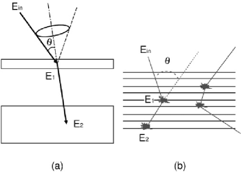
In a Compton telescope, an incident gamma-ray photon is scattered in the scattering part of the detector and the Compton-scattered photon is absorbed in the absorber part (see Fig. 1(a)). The scattering angle of the incident gamma-ray is then written as,
| (1) |
where is the energy of the recoil electron in the scattering detector and is the energy deposited in the absorbing detector. Thus, by measuring the energy and position of the individual interactions, we can limit the direction of the incident photon to the surface of a cone. The projection of this cone onto the celestial sphere is the “event circle”. The -ray source is located at the point of the intersection of all event circles. As clearly seen in the equation, the angular resolution becomes better if the energy resolution becomes higher.
Since the major goals for the next generation Compton telescope are to increase the detection efficiency by up to two orders of magnitude over the COMPTEL and to realize much improved background rejection, the development of 3-D position sensitive detectors with a high detection efficiency, a high angular resolution and an excellent energy resolution is the key. Several detector options are under consideration, including the use of position-sensitive solid state detectors such as germanium and silicon[4, 5, 6, 7, 8, 9, 10, 11, 12]. As to applications to nuclear medicine, see D. Meier et al.[13] and references therein.
We have been working on a semiconductor Compton telescope based on silicon and cadmium telluride (Si/CdTe Compton camera) in view of sub-MeV to MeV detectors with high sensitivity[11, 12]. In this paper, we demonstrate the first results from a prototype Si/CdTe Compton camera. Firstly we describe the performance of newly-developed CdTe pixel detectors which are used as the absorber part of the prototype. Secondly, the reconstruction of the scattering angle and a polarization measurement are reported based on experiments at the SPring-8 synchrotron radiation facility in Japan. Further report on the imaging performance of the Si/CdTe Compton camera will be described in a separate paper[14].
II Si/CdTe Compton camera
In the Si/CdTe Compton camera, a stack of many thin scatterers made of fine pitch double-sided Si strip detectors is used to record the Compton scatterings. Additional layers made of a heavy semiconductor such as CdTe (or CdZnTe) are used to absorb the Compton scattered photons. The order of the interaction sequences, hence the correct energy and direction of the incident photon, can be reconstructed by examination of the energy-momentum conservation for all possible sequences (Fig. 1(b)).
For imaging devices, their good energy resolution and the ability to fabricate compact arrays are very attractive features of semiconductor detectors in comparison with inorganic scintillation detectors. The high density and good detection efficiency of CdTe and CdZnTe, comparable with that of NaI(Tl) and CsI(Tl), are important additions when we design the absorber part of the Compton telescope [11]. Based on our recent developments, the CdTe diode now shows an energy resolution comparable with that of a Ge detector, even at room temperature[15, 16, 17]. The energy resolution achieved for a planar diode detector, which has dimensions of 2 mm 2 mm as an active area and a thickness of 0.5 mm, is 0.93 keV and 1.2 keV (FWHM) at 59.5 keV and 122 keV, respectively.
The merit of using Si as scatterers in the energy range from 50 keV up to several hundred keV is that the cross section of Compton scattering is well above that of photoelectric absorption. Therefore the efficiency of Compton scattering is high if the scattering part has sufficient thickness. Additionally, Si works better than CdTe in terms of the “Doppler broadening” effect. The standard Compton formula Eq. (1) assumes the scattering takes place with a free electron at rest. When we take the momenta of bound electrons into account, we need to consider additional uncertainties in the energy and angle of the scattered gamma ray[18]. This phenomenon is often referred to as Doppler broadening. The additional uncertainties on the energy resolution and angular resolution are especially pronounced at low gamma ray energies and become less significant as the atomic number decreases. Together with the high absorption efficiency of CdTe, a Si/CdTe Compton camera can be used efficiently below several hundred keV in particular. Application of a stack of Si detectors to higher -ray energies, where multiple Compton scattering has to be taken into account, is described in [4, 5, 11].
III High resolution CdTe pixel detector and Double-sided Si Strip Detector
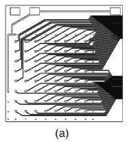
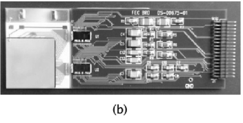
As a key component of a Si/CdTe Compton camera, we have developed a CdTe pixel detector (Fig. 2(b)). It is made of a CdTe diode and has the dimensions of 16.5 mm 16.5 mm as an active area, surrounded by a 1 mm wide guard-ring, and a thickness of 0.5 mm. On the cathode side, it is pixellated with 2 mm square electrodes. The gap between pixels is 50 m. A fanout board, which consists of bump pads and patterns to route the signal from pads on the surface of the ceramic board, is shown in Fig. 2(a). Once each pixel electrode on the CdTe diode is connected to the bump pad, we can extract signals from the detector. The leakage current of this device is 200 pA/pixel at a bias voltage of 600 V and a temperature of 20 . For the readout of many channels from the detector, we utilize a newly developed low noise analog ASIC, “VA32TA” [19, 20]. We handle 64 channels as a module and read out with the Front End Card (FEC) on which two VA32TAs are mounted.
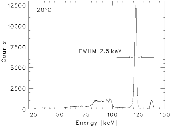
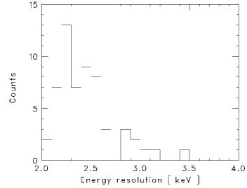
We developed a first prototype detector and obtained spectra from each channel. Fig. 3 shows the sum of the energy spectra for all channels except for seven channels at the corner in which no signal was obtained. The detector is operated at room temperature (20 ) under the bias voltage of 600 V. We obtain an energy resolution of 2.5 keV (FWHM) for the 122 keV -ray lines. Fig. 4 shows the distribution of the energy resolution of all channels. It ranges from 2.1 to 3.4 keV. When the operating temperature is 0 , the highest energy resolution of 1.7 keV at 60 keV is obtained.
Although we have demonstrated that our bump method provides high yield when we handle small pixel size[22, 21], no signal was obtained for seven channels out of 64 of the first detector due to a failure in the procedure of connecting the pixels to the fanout board. To improve the yield of the connections, we have fabricated another batch of detectors in different conditions of bump bonding. In this version, the yield of the connections has increased to 99.6%, but the energy resolution deteriorates to 6 keV under the same operating conditions at 20 . We are working to improve this performance. Despite the relatively poor energy resolution, we use detectors from the second batch in the following experiment because they provide larger acceptance than the case for the first batch.
Another key component is the low noise double-sided Si strip detectors(DSSDs). The DSSD used in the present detector has a thickness of 300 m and the strips have a length of 2.56 cm on each side. The strip pitch of DSSD is 800 m and the strip gap is 100m. The signals are also processed via the same FECs as the CdTe pixel detectors. See Tajima et al. for details on DSSD developments [19, 20].
IV Prototype of Si/CdTe Compton Camera and its Performance
IV-A Setup
To demonstrate the concept of the Si/CdTe Compton camera, two CdTe 88 pixel detectors are combined with one DSSD. In Fig. 5(a), we present a schematic view of the arrangement of the detectors. In this configuration, photons scattered in the DSSD are absorbed by the CdTe detectors if the scattering angle is between 100∘ and 130∘. This geometry is adopted because the scattered photons have relatively low energy and can be photo-absorbed efficiently in CdTe.
The CdTe detectors used in the prototype have an energy resolution of about 7 keV on average when we operate at a temperature of 25 with a bias voltage of 500 V. The energy resolution of the DSSD used in this system is 5 keV at a temperature of 25 . The resolution is deteriorated due to the rather high operation temperature. As to the DSSD, “RC chips”, which provides bias voltage via polysilicon bias resistors and AC-coupling between each strip and the input of VA32TA, could also be the cause of the degradation of the spectra. Another type of DSSD we have developed with a strip pitch of 400 m has achieved an energy resolution of 1.3 keV at a temperature of 0 without “RC chips” [19, 20].
Two CdTe pixel detectors and a DSSD are read out together by the specially designed compact readout system including an ADC, which is controlled with a fast serial interface, “Space Wire (IEEE 1355)”[23]. During data acquisition, events are taken when trigger signals are generated from CdTe pixel detectors. The data from triggered CdTe detectors and the DSSD are read out.
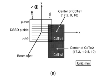
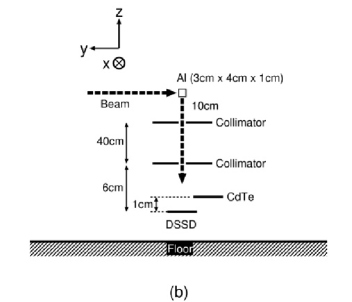
We conducted a photon beam experiment at the synchrotron radiation facility, “SPring-8” [24] in Japan on 7 July, 2003. The initial beam energy was 270 keV. To reduce the intensity of the original beam, the beam was scattered by an Al plate. Photons scattered at 90∘ are collimated with Pb collimators as an input to the Compton camera (Fig. 5(b)). According to the Compton kinematics, the estimated incident energy at the detector is 177 keV and the incident photons are nearly 100 % linearly polarized. The electric vectors of the photons are parallel to the p-strips of the DSSD. We irradiated the photon beam with the geometry shown in Fig. 5(a). After a irradiation, the whole Compton camera system is rotated by 90∘ around the z-axis. By performing this procedure four times, we obtain 360∘ coverage. During the experiment, the noise of n-strips of the DSSD was high and we can not use the information from the n-strips. We estimate the hit channel of the n-side on the basis of geometrical information of the collimator and fix the hit channel in the following analysis.
IV-B Reconstruction of Compton scattering angle
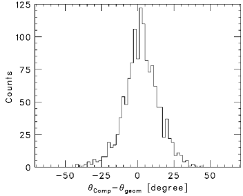
From the data obtained, we reconstruct the Compton scattering angle. Fig. 6 shows the distribution of for the events under the conditions 150 keV 180 keV, keV and . Here, , are the energy deposited in the DSSD and the CdTe detectors, respectively. The scattering angle is calculated from Eq. (1) using , while is that calculated from the hit positions under the assumption that the incident beam is orthogonal to the DSSD surface. The FWHM of the peak in Fig. 6, i.e. the angular resolution of the Compton camera, is 22∘. This value is consistent with the angular resolution of 20∘ obtained from an EGS4 Monte Carlo simulation[25] with a low energy extension[26]. From the analysis of the simulation, the contribution to this angular resolution of the detector positional resolution is estimated to be 6.2∘, that of the energy resolution 17∘, and that of Doppler broadening 4.7∘.
Although the basic performance of a Si/CdTe Compton camera is demonstrated, the angular resolution is not so pronounced. If the energy resolution of both the DSSD and CdTe pixel detectors reaches their present best value, 1.3 keV and 2.5 keV, respectively, the contribution of the energy resolution can be reduced to 3-4∘. For the geometrical contribution, improvement of positional resolution can be achieved either by using smaller pitch devices or by increasing the distance between the DSSD and CdTe detectors. Note that the relatively large Doppler broadening contribution is only because of the low incident gamma-ray energy and there is no semiconductor currently, except for diamond, with better performance.
IV-C Performance as a polarimeter
An important feature of the Compton camera is the capability of measuring polarization[27]. The differential cross-section of Compton scattering is expressed as
| (2) |
Here, is the scattering angle, is the azimuthal angle of the scattered photon with respect to the electric vector of the incident photon, and is the classical electron radius. As shown in Eq. (2), photons are likely to be scattered in a direction orthogonal to their electric vector. Therefore the distribution of scattered photons provides information of the linear polarization of incident photons.
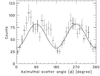
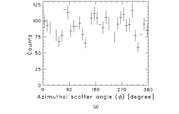
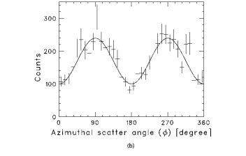
The azimuthal scattering angle () distribution of the experiment is shown in Fig. 7 and an angular modulation is clearly observed. To correct the geometrical effect related to the layout of the detectors and the associated quantization of possible scattering angle, the measured distribution is normalized by the model distribution (Fig. 8(a)) estimated from an EGS4 Monte Carlo simulation for an unpolarized beam. Thus, Fig. 7 includes the statistical error of both the experiment and simulation. For comparison, a distribution obtained from the results of a simulation with a 100% linearly polarized beam is shown in Fig. 8(b), which is corrected in the same way as the actual data. In the simulation, 108 photons are incident on the detector and 6.3102 photons undergo one Compton scattering followed by photoelectric absorption. The low efficiency shown here must be improved by stacking Si and CdTe detectors.
V Conclusion
The hard X-ray and -ray bands are important frequency windows for exploring the energetic universe. It is in these energy bands that non-thermal emission becomes dominant. In order to study the “non-thermal universe”, characterized by accelerated high energy particles, we need an advanced mission which has orders of magnitude better sensitivity than any previous or current missions. To this end, we are working on a Si/CdTe Compton Camera. With two CdTe pixel detectors and a DSSD, we have constructed a prototype Si/CdTe Compton camera. Using the prototype, we conducted a photon beam experiment and demonstrate the concept of Si/CdTe Compton camera. The angular resolution is 22∘ which is limited by the energy resolution of 7 keV for the CdTe pixel detector and 5 keV for the Si detector employed in this camera. By employing devices with a better energy resolution, the angular resolution is expected to be improved significantly. As the first demonstration of the Si/CdTe Compton camera as a gamma-ray polarimeter, we have measured polarization by using a synchrotron photon beam. We have succeeded to obtain a very clear modulation pattern. The polarimetric modulation factor is measured to be 43%. Based on these results, a semiconductor Compton telescope utilizing Si and CdTe is shown to posses a potential as both a Compton camera and a polarimeter.
Acknowledgment
The authors would like to thank P. G. Edwards and C. Baluta for their critical reading of the manuscript.
References
- [1] V. Schönfelder, A. Hirner, K. Schneider, “A telescope for soft gamma ray astronomy,” Nucl. Instrum. Methods, vol. 107, pp. 385-394, 1973.
- [2] D. Herzo, R. Koga, W. A. Millard, S. Moon, J. Ryan, R. Wilson, A. D. Zych, and R. S. White, “A large double scatter telescope for gamma rays and neutrons,” Nucl. Instrum. Methods, vol. 123, pp. 583-597, 1975.
- [3] V. Schönfelder, H. Aarts, K. Bennett, H. de Boer, J. Clear and W. Collmar, et al., “Instrument description and performance of the imaging gamma-ray telescope COMPTEL abroad the Compton Gamma-Ray Observatory,” Astrophys. J. Suppl. Series, vol. 86, pp. 657-692, 1993.
- [4] T. Kamae, R. Enomoto and N. Hanada, “A new method to measure energy, direction, ans polarization of gamma rays,” Nucl. Instrum. Methods, vol. A 260, pp. 254-257, 1987.
- [5] T. Kamae, N. Hanada and R. Enomoto, “Prototype design of multiple Compton gamm-ray camera,” IEEE Trans. Nucl. Sci., vol. 35, pp. 352-355, 1988.
- [6] Recommended priorities for NASA’s gamma ray astrophysics program, NP-1999-04-072-GSFC.
- [7] J. D. Kurfess, W. N. Johnson, R. A. Kroeger, B. F. Phlips and E. A. Wulf, “Development and applications of position-sensitive solid-state gamma ray detectors,” Nucl. Instrum. Methods, vol. A 505, pp. 256-264, 2003.
- [8] G. Kanbach, R. Andritschkea, F. Schoppera, V. Schönfeldera, A. Zoglauera, P. F. Bloserb, S. D. Hunterb, J. A. Ryanc, M. McConnellc, V. Reglerod, G. DiCoccoe and J. Knödlseder, “The MEGA project,” New Astronomy Reviews, Vol. 48, pp. 275-280, 2004.
- [9] T. J. O fNeill, D. Bhattacharya, M. Polsen, A. D. Zych, J. Samimi and A. Akyuz, “Development of the TIGRE Compton telescope for intermediate-energy gamma-ray astronomy,” IEEE Trans. Nucl. Sci., vol. 50, pp. 251-257, 2003.
- [10] Y. F. Du, Z, He, G. F. Knoll, D. K. Wehe, W. Li, “Evaluation of a Compton scattering camera using 3-D position sensitive CdZnTe detectors,” in Proc. SPIE, vol. 3768, 1999, pp. 228-238.
- [11] T. Takahashi, K. Nakazawa, T. Kamae, H. Tajima, Y. Fukazawa, M. Nomachi and M. Kokubun, “High resolution CdTe detectors for the next generation multi-Compton gamma-ray telescope,” in Proc. SPIE, vol. 4851, 2003, pp. 1228-1235.
- [12] T. Takahashi, K. Makishima, Y. Fukazawa, M. Kokubun, K. Nakazawa, M. Nomachi, H. Tajima, M. Tashiro and Y. Terada, “Hard X-ray and gamma-ray detectors for the NEXT mission,” New Astronomy Reviews vol. 48 pp. 269-273, 2004.
- [13] D. Meier, A. Czermak, P. Jalocha, B. Sowicki, M. Kowal, W. Dulinski, G. Mæhlum, E. Nygård, K. Yoshioka, J. Fuster, C. Lacasta, M. Mikuz, S. Roe, P. Weilhammer, C.-H. Hua, S.-J. Park, S. J. Wildermann, L. Zhang, N. H. Clinthorne, and W. L. Rogers, “Silicon detector for a Compton camera in nuclear medical imaging,” IEEE Trans. Nucl. Sci., vol. 49, pp. 812-816, 2002.
- [14] T. Tanaka et al., “Development of a Si/CdTe semiconductor Compton telescope,” in Proc. SPIE, vol. 5501, to be published in 2004.
- [15] T. Takahashi and S. Watanabe, “Recent progress on CdTe and CdZnTe detectors,” IEEE Trans. Nucl. Sci., vol. 48, pp. 950-959, 2001.
- [16] T. Tanaka, Y. Kobayashi, T. Mitani, K. Nakazawa, K. Oonuki, G. Sato, T. Takahashi and S. Watanabe, “Recent achievements of the high resolution Schottky CdTe diode for -ray detectors,” New Astronomy Reviews, vol. 48, pp. 309-313, 2004.
- [17] K. Nakazawa, K. Oonuki, T. Tanaka, Y. Kobayashi, K. Tamura, T. Mitani, G. Sato, S. Watanabe, T. Takahashi, R. Ohno, A. Kitajima, Y. Kuroda and M. Onishi, “Improvement of the CdTe diode detectors using a guard-ring electrode,” IEEE Trans. Nucl. Sci., to be published in 2004.
- [18] A. Zoglauer and G. Kanbach, “Doppler broadening as a lower limit to the angular resolution of next-generation Compton telescopes,” in Proc. SPIE, vol. 4851, 2003, pp. 1302-1309.
- [19] H. Tajima, T. Kamae, S. Uno, T. Nakamoto, Y. Fukazawa, T. Mitani, T. Takahashi, K. Nakazawa, Y. Okada and M. Nomachi, “Low noise double-sided silicon strip detector for multiple-Compton gamma-ray telescope,” in Proc. SPIE, vol. 4851, 2003, pp. 875-884.
- [20] H. Tajima, T. Kamae, G. Madejski, E. do Couto e Silva, S. Uno, T. Nakamoto, Y. Fukazawa, T. Mitani, T. Tanaka, T. Takahashi, K. Nakazawa, Y. Okada, M. Nomachi and D. Marlow “Performance of a low noise front-end ASIC for Si/CdTe detectors in multiple-Compton gamma-ray telescope,” IEEE Trans. Nucl. Sci., to be published in 2004.
- [21] T. Takahashi, S. Watanabe, M. Kouda, G. Sato, Y. Okada, S. Kubo, Y. Kuroda, M. Onishi, and R. Ohno, “High-resolution CdTe detector and application to imaging devices,” IEEE Trans. Nucl. Sci., vol. 48, pp. 287-291, 2001.
- [22] M. Löcker, P. Fischer, M. Kouda, S. Krimmel, H. Krüger, M. Lindner, K. Nakazawa, T. Takahashi, and N. Wermes, “Single photon counting X-ray imaging with CdTe- and Si- multichip pixel modules,” IEEE Trans. Nucl. Sci., to be published in 2004.
- [23] T. Mitani, H. Nakamura, S. Uno, T. Takahashi, K. Nakazawa, S. Watanabe, H. Tajima, M. Nomachi, Y. Fukazawa, S. Kubo, Y. Kuroda, M. Onishi and R. Ohno, “Large area gamma-ray imaging detector based on high resolution CdTe diode,” IEEE Trans. Nucl. Sci., vol. 50, pp. 1048-1052, 2003.
-
[24]
Japan Synchrotron Radiation Research Institute,
“SPring-8 Beamline Handbook,”
Available: http://www.spring8.or.jp/e/publication-5-e.html - [25] W. R. Nelson, H. Hirayama and D. W. O. Rogers, “The EGS4 code system,” SLAC-Report-265, 1985.
- [26] Y. Namito and S. Ban and H. Hirayama, “Implementation of linearly-polarized photon scattering into the EGS4 code,” Nucl. Instrum. Methods, vol. A 332, pp. 277-283, 1993.
- [27] F. Lei, A. J. Dean and G. L. Hills, “Compton polarimetry in gamma-ray astronomy,” Space Science Reviews, vol. 82, pp. 309-388, 1997.