Development of a Si/CdTe semiconductor Compton telescope
Abstract
We are developing a Compton telescope based on high resolution Si and CdTe imaging devices in order to obtain a high sensitivity astrophysical observation in sub-MeV gamma-ray region. In this paper, recent results from the prototype Si/CdTe semiconductor Compton telescope are reported. The Compton telescope consists of a double-sided Si strip detector (DSSD) and CdTe pixel detectors, combined with low noise analog LSI, VA32TA. With this detector, we obtained Compton reconstructed images and spectra from line gamma-rays ranging from 81 keV up to 356 keV. The energy resolution is 3.8 keV and 7.9 keV at 122 keV and 356 keV, respectively, and the angular resolution is and at 122 keV and 356 keV, respectively.
keywords:
gamma-ray, Compton telescope, semicondictor detector, CdTe, Silicon Strip Detector1 Introduction
Gamma-ray universe in the energy band of 100 keV to 10 MeV is a good observational window to study nucleosynthesis and particle acceleration in high energy astrophysical objects. However, in this energy band, observation sensitivity have been still limited, due to high background, difficulty in detecting photons, and incapability of imaging. A Compton telescope tracking the Compton scattering process of gamma-rays by position and energy sensitive detectors is difficult but a promising approach to bring a breakthrough in this energy band.
In the MeV region, COMPTEL[1] on-board CGRO (Compton Gamma-Ray Observatory) was the first successful Compton telescope and brought many pioneering results[2]. In a Compton telescope, deposited energy and position of the gamma-ray interactions with the detector are acquired. When a gamma-ray photon is scattered in one detector and absorbed in another detector, the incident energy of the gamma-ray and the scattering angle can be determined as,
| (1) | |||||
| (2) |
where is the energy of the recoil electron, is the energy of the scattered photon and is the scattering angle. The latter equation presents the incident direction as a cone in the sky.
As shown in equation (2), incident direction of a gamma-ray is calculated from the position and the energy information of interactions. Therefore, employing semiconductor imaging spectrometers as components of Compton telescopes, with their good energy and position resolution, will drastically improve the angular resolution and hence the sensitivity. In this point of view, advanced Compton telescopes based on Si, Ge, CZT and CdTe are proposed and development is on-going in many groups[3, 4, 5, 6, 7, 8]. A Compton telescope also enables us to measure polarization of gamma-rays, by obtaining the azimuthal distribution of Compton scattering[9, 10].
Based on our CdTe and Si detector technologies[11, 12, 13, 14, 15], we are working on a new Si/CdTe semiconductor Compton telescope to explore the universe in the energy band from 100 keV to a few MeV. In this paper, we describe experimental results obtained with a prototype Compton telescope which consists of one layer of a Double-sided Si strip detector (DSSD) and one layer of CdTe pixel detectors. Detailed performance of the DSSD and the vision of next-generation gamma-ray missions using this technique are reported elsewhere[14, 16]. Demonstration of polarization detection are reported in Mitani et al.[17] and Tajima et al.[18]
2 Si/CdTe semiconductor Compton Telescope
Basic concept of Si/CdTe Compton telescope is to utilize Si as a scatterer and CdTe as an absorber[4, 17]. Compared to Compton telescopes using scintillator as an absorber, this design improves the performance especially at sub-MeV region, as low as 100 keV. The lower energy coverage is prefered to connect the band pass of Compton telescope with that of the technology using hard X-ray focusing mirror optics[19, 20].
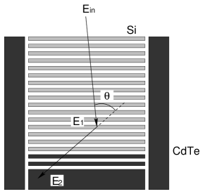
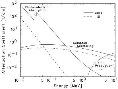
A schematic image of Si/CdTe Compton telescope is shown in Figure 1. The major interaction process of Si with gamma-rays with energy higher than 60 keV is Compton scattering, while in CdTe photo-electric absorbtion is still dominant up to 300 keV (Figure 2). In a Si/CdTe Compton telescope, therefore, “one-Compton and absorption” events dominate the data around several hundred keV. A merit of utilizing this kind of event is that it is relatively easy to analyze. For example, in Compton scattering of photons with energy less than keV, the recoil electron energy is always less than that of the scattered photon[3]. In addition, the ambiguity in the Compton scattering angle caused by the orbital motion of bound electron is relatively small for Si compared to that of Ge and CdTe. This effect is called “Doppler broadening effect[21]”, and is the dominant factor of angular resolution around a few hundered keV.
The demerit of current Si/CdTe Compton telescope design is that it looses effective area especially at the higher energy band, as much as a few MeV. This is simply because the density of Si () is much less than that of CdTe (). For Compton telescope aiming mainly at a few MeV band, increasing the number and thickness of CdTe layers becomes important.
3 Experimental setup
Two key technologies for our Si/CdTe Compton telescope are DSSD and CdTe pixel detectors. In this section, we describe the detail of the newly developed CdTe pixel detector and design of the prototype Compton telescope. Detail of the DSSD development is described in Fukazawa et al.[14]
3.1 The CdTe Pixel Detector
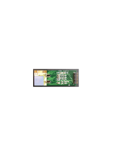
The CdTe pixel detector is based on the Schottky CdTe diode device, utilizing indium as the anode and platinum as the cathode. This device is developed with ACRORAD, Japan and characterized by its low leakage current and high uniformity[11, 22]. Figure 3 (left) shows the photo of the detector. The detector has dimensions of and a thickness of . The indium side is used as a common electrode and the platinum side is divided into 8 by 8 pixels and a guard ring with a width of 1 mm. The guard-ring electrode are attached to reduce the leakage current of the side and corner pixels because most of the leakage current is through the detector perimeter[12, 13]. Pixel size is , and the gap between each pixel is .
Each pixel is connected to a fanout board by bump bonding technology developed in cooperation with Mitsubishi Heavy Industry, Japan[23]. Since the leakage current of each pixel is as low as at a bias voltage of 500 V even at room temperature, the signal lines are directly connected to the input of readout electronics, an analog LSI VA32TA[15, 24]. This LSI is developed with IDEA, Norway, and characterized by its low noise. The LSIs are read out via specially designed compact readout system including an ADC and FPGA, which is controlled with a fast serial interface ”Space Wire (IEEE 1355)”[25].
Figure 3 (right) shows a spectrum of obtained with the CdTe pixel detectors employed in the prototype Compton telescope. In these detectors, all 128 channels are properly connected and their spectra are summed after gain correction. The data is measured at a temperature of and with a bias voltage of 500 V. The energy resolution is 3.2 keV (FWHM) for the 122 keV peak.

3.2 The prototype Compton Telescope System
The prototype Si/CdTe Compton telescope consists of two CdTe pixel detectors and a DSSD. The DSSD has a thickness of . There are 64 strips with a length of 2.53 cm in both sides oriented orthogonally. The strip pitch is and the gap between the strips is . By reading out both the p-strips and n-strips, we can obtain two-dimensional positional information. The device is also read out with VA32TA. The p-strips are connected directly to the input of the LSI, and the n-strips are connected via coupling capacitors. To fully deplete the device, the n-side is biased with a voltage of 110 V. Because the spectral resolution of the p-side is better than that of the n-side, we obtained spectra only from the p-strips, and data from the n-strips are used for the positional information. Figure 4 shows a spectrum of obtained with the p-strips of the DSSD operated at a temperature of . The energy resolution for 81.0 keV peak is 1.9 keV (FWHM).
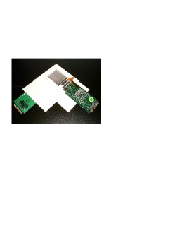
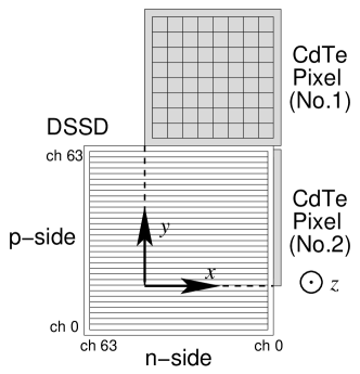
Figure 5 presents the arrangement of two CdTe pixel detectors and the DSSD at our Compton telescope. The separation between the DSSD layer and the CdTe layer is 12.5 mm. In the following experiment, we kept the whole detector system at a temperature of . We irradiated gamma-ray sources of and which were placed 353 mm above the surface of the DSSD. Triggers only from the LSIs connected to the CdTe detectors were enabled. When a trigger was generated from some channel, all channels connected to the CdTe detector which issued the trigger and all channels connected to the DSSD are read out.


4 Data analysis
4.1 Compton Reconstruction of Images
Data reduction is performed as follows. First,“two-hit events”, one hit in DSSD and one hit in CdTe, were selected from the raw data. Here, one hit in DSSD means that only one channel that is connected to DSSD has a pulse hight above 6 keV, and one hit in CdTe detectors means that only one channel that is connected to CdTe detectors has a pulse hight above 20 keV.
A scatter plot of the energy deposit at the DSSD () and at the CdTe detectors () is shown in Figure 6. This plot is obtained when we irradiated to the Compton telescope. There are branches which satisfies and . These branches are the events in which incident gamma-rays of 122 keV or136 keV are scattered in one detector and then absorbed in the other. Another noticeable branches are those parallel to the horizontal axis around –. These are the events by the fuorescence X-rays from Cd (: 23.1 keV, : 26.1 keV) and Te (: 27.4 keV, : 31.0 keV) which escape from the CdTe detectors and are absorbed in the DSSD, and not the Compton events.
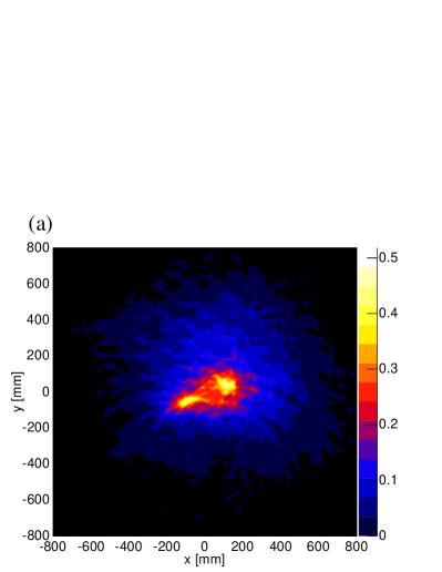
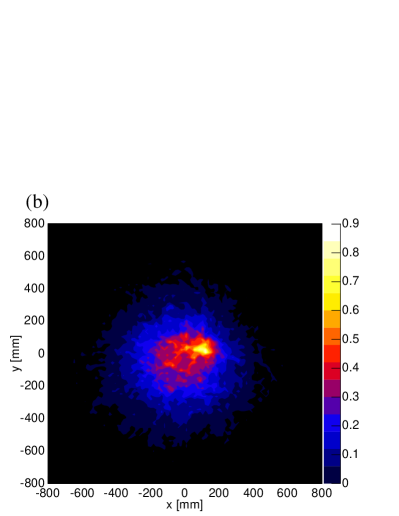
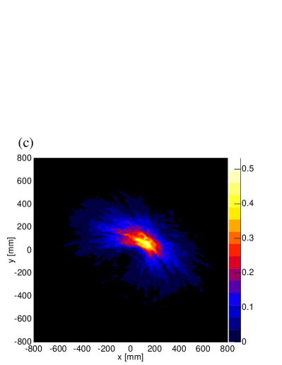
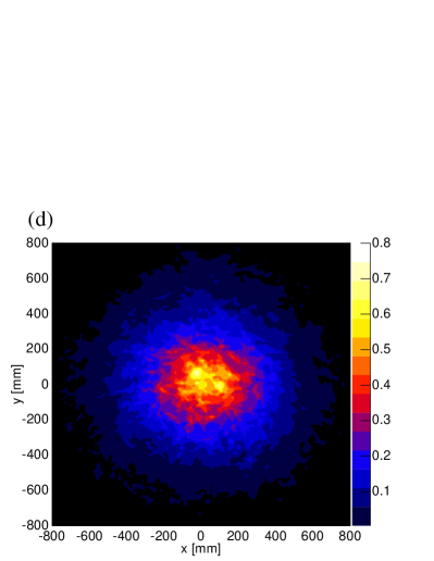
For these “two-hit events”, we calculated the Compton-scattering angle by using equation (2). In the calculation, we assumed that incident gamma-rays are scattered in the DSSD and absorbed in the CdTe pixel detector. From the calculated scattering angle and the two hit positions, the Compton cones are drawn on the sky event by event. We projected the cone at the plane at the distance of 353 mm, and obtained the image of the gamma-ray source. Figure 7 shows the images obtained with the experimental data, in which the gamma-ray source position can be clearly identified.
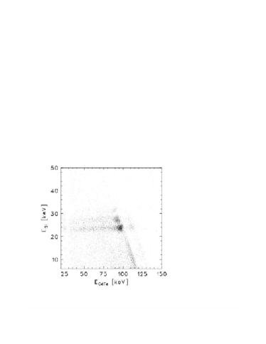
Figure 7(a) is obtained by irradiating gamma-rays from two sources. These sources are placed 230 mm separate from each other, which corresponds to at the distance of 363 mm. The image is obtained by selecting events in which sum of the energy deposit at the DSSD and the CdTe detectro is within .
For the images, energy selection is above 250 keV and for Figure 7(b) and (c), respectively. In Figure 7, appearance of each image is different. This reflects the basic process and geometry of the detector. For example, 81 keV image has a peculiar “batterfly-like” shape. This is caused by the fact that the scattering angle must be larger than to deposit an energy larger than 6 keV at the DSSD, which is the energy threshold in this analysis, and that Compton cones with peculiar orientation are obtained because the CdTe detectors are offset from the DSSD. Another impressive image is obtained when we select the energy band of 100–250 keV for irradiation data (Figure 7(d)). Compared with line images (Figure 7(b) and (c)), the location of source is not clear. This is because the image is dominated by back scattered events and “Compton-Compton” events which finally escaped from the detector. From this data, we see that it is better to use thicker CdTe detector and, if possible, utilize a surrounding shield counter to identify the physical process of each event.
4.2 Angular Resolution
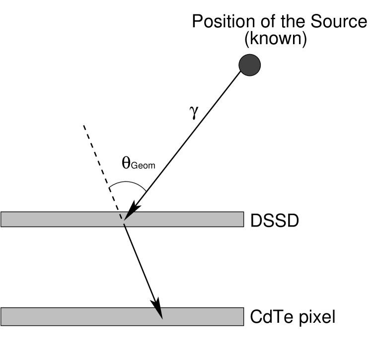
In order to evaluate angular resolution of our prototype Compton telescope, we compare the calculated Compton-scattering angles () with those defined by the location of gamma-ray source and hit positions () (see Figure 9). The difference between the two values reflects the angular resolution of Compton telescope.
We examined the distribution of for various peaks of (122 keV and 136 keV) and (81.0 keV, 303 keV and 356 keV). Figure 9 shows the example of 122 keV events. The FWHM of these distributions (), which is the angular resolution of the Compton telescope, is plotted against the incident gamma-ray energy in Figure 10. The angular resolution obtained from Geant4 Monte Carlo simulations[26], using the Compton scattering process, G4LECS[27, 28] are also plotted. The experimental results are consistent with the results from the simulation.
As shown in Figure 10, the angular resolution becomes better as the incident gamma-ray energy becomes higher. For example, at 81.0 keV and at 356 keV. In order to examine the reason of this tendency, we estimated the contribution of position and energy resolution of the DSSD and the CdTe detector. Contribution of position resolution () is estimated by using the actual hit positions obtained from the experiment and the strip/pixel size of the DSSD and the CdTe detector. To estimate the contribution of energy resolution (), we used the Compton-scattering angles of actual events and smoothed them with detector energy resolution. In Figure 10, the estimated values are plotted. In the same Figure, the values of
| (3) |
are also plotted. This can be interpreted to be the contribution of Doppler broadening, which is supported by the fact that the experimental data is consistent with those obtained from simulations. As seen in Figure 10, and becomes smaller as the incident energy becomes higher, whereas becomes larger. The tendency of is consistent with that of Monte Carlo simulations in several papers (e.g. Zoglauer and Kanbach 2003[21]). becomes smaller when the incident gamma-ray energy is smaller, because in such events only larger scattering angle and hence the longer distance events can be reconstructed due to the energy threshold for the DSSD (6 keV).
In order to investigate the relation between the scattering angles and the angular resolution, we plotted the angular resolution against Compton scattering angle from data in Figure 11. The estimated value of uncertainty due to position resolution, energy resolution and Doppler broadening are obtained in the same way as Figure 10 and plotted together. The value of is somewhat larger for larger scattering angles, and our analysis shows that this tendency is caused by Doppler broadening. In other words, the contribution of Doppler broadening can be reduced if we can reconstruct the events with smaller scattering angles, which means lower energy threshold for the DSSD.


4.3 Compton Reconstruction of Spectra
Energy spectra of the incident gamma-rays are obtained by summing deposited energy at the DSSD and the CdTe detector as shown in equation (1). The dotted lines in Figure 12 show the spectra which we obtained by simply summing the deposited energy at each detector for all “two-hit events”. In these spectra, the gamma-ray peaks from the sources can not be clearly identified since we can not distinguish “one-Compton and absorption events” from other “two-hit events”, such events in which gamma-rays are scattered in the DSSD and scattered again in the CdTe and so on. Then we performed event selection by Compton kinematics. We selected the events satisfying . The solid lines in Figure 12 show the spectra of gamma-rays from and after this selection. In these spectra, the gamma-ray peaks from the source are relatively enhanced.
The energy resolution is 3.8 keV (FWHM) for 122 keV gamma-rays and 7.6 keV for 356 keV. These values are generally consistent with the energy resolution of the DSSD (1.9 keV) and the CdTe pixel detectors (3.2 keV for 122 keV and 7.5 keV for 356 keV) under this setup, i.e. the energy resolution of this Compton telescope is expressed as
| (4) |
where and are the energy resolution of the DSSD and the CdTe detector, respectively.


4.4 Compton Reconstruction of K-escape Events
As described above, significant number of fluorescence X-rays from the CdTe detectors are detected in the DSSD due to high fluorescence yield of Cd and Te ( for the K shell). Depending on the detector geometry, K-escape events can share significant ratio in total events. Therefore, we attempted to reconstruct events in which photons are scattered at the DSSD, absorbed at the CdTe, K-escape takes place and the fluorescence line is detected again in the DSSD.
First, we selected three-hit events, twice in the DSSD and once in the CdTe detector. Then we further select the events in which one of the deposited energy in the DSSD is between 20 keV and 34 keV. After adding these measured value to the energy observed in the CdTe detector, we calculated the Compton-scattering angle as the usual two-hit events. Figure 13 (right) shows a spectrum of obtained from this analysis. Only the events which satisfy are selected. The peak around 122 keV is clearly identified.


5 Implications from the prototype
From §4.2, it is clear that the angular resolution of the prototype Compton telescope can be improved if the energy resolution becomes better especially for lower energy and if the position resolution becomes better for higher energy. In view of energy resolution, the CdTe detectors used in the prototype Compton telescope are not satisfactory. Actually, the best channel in other detector with the same design shows an energy resolution of 1.7 keV. We are currently trying to improve this properties by optimizing parameters for bump bonding. Figure 14 shows the sum spectrum of all channels of the latest version of CdTe pixel device, obtained at with a bias voltage of 600 V. An energy resolution of 2.4 keV (FWHM) at 122 keV is obtained with the detector. Development of CdTe pixel detectors with smaller pixel size is also in underway[29]. If we can make the pixel size smaller, we will improve not only the position resolution but also the energy resolution since the capacitance and the leakage current per pixel can be reduced. However, we need to be careful for charge sharing or K-escape to the other pixels in smaller pixel size detectors.
Obtaining higher detection efficiency is another crucial issue for the next version of the Compton telescope. Currently, we are working on two directions. One is to make a multi-layer DSSD, up to 24 layers or more. Another way is to improve the thickness of the detector. We are now developing thick DSSD and thicker CdTe pixel detectors up to 5 mm.

6 Conclusion
Si/CdTe semiconductor Compton telescope is attractive to explore the universe in sub-MeV gamma-ray region. We constructed a prototype Compton telescope which consists of one layer of DSSD and one layer of CdTe pixel detectors. With this prototype detector, we succeeded in Compton reconstruction of images and spectra in the energy band from 80 keV to 400 keV. The obtained angular resolution is and at 122 keV and 356 keV, respectively, and the energy resolution is 3.6 keV (FWHM) at 122 keV and 7.6 keV (FWHM) at 356 keV. The lower energy coverage down to 80 keV owes to good energy resolution and lower energy threshold of our detectors. We also succeeded in reconstruction of three-hit events by Compton scattering and K-escape, which becomes significant under some configuration of Compton telescopes. With these results, we have experimentally demonstrated the high capabilities of a Si/CdTe Compton telescope.
References
- [1] V. Schönfelder et al., “Instrument description and performance of the imaging gamma-ray telescope COMPTEL aboard NASA’s Compton Gamma Ray Observatory”, ApJ Suppl., 86, pp. 657–692, 1993.
- [2] V. Schönfelder et al., “COMPTEL overview: Achievements and expectations”, Astron. Astrophys. Suppl., 120, pp. 13–21, 1996.
- [3] T. Takahashi et al., “Hard X-ray and -ray Detectors for the NEXT mission”, New Astronomy Reviews, 48, pp. 269–273, 2004.
- [4] T. Takahashi et al., “High resolution CdTe detectors for the next generation multi-Compton gamma-ray telescope”, Proc. SPIE, 4851, pp. 1228–1235, 2003.
- [5] G. Kanbach et al., “The MEGA project,” New Astronomy Reviews, 48, pp. 275–280, 2004.
- [6] J. D. Kurfess et al., “Development and applications of position-sensitive solid-state gamma ray detectors ,” Nucl. Instrum. Methods, A505, pp. 256–264, 2003.
- [7] T. J. O’Neill et al., “Development of the TIGRE Compton telescope for intermediate-energy gamma-ray astronomy,” IEEE Trans. Nucl. Sci., 50, pp. 251–257, 2003.
- [8] Y. F. Du et al., “Evaluation of a Compton scattering camera using 3-D position sensitive CdZnTe detectors,” in Proc. SPIE, 3768, 1999, pp. 228–238.
- [9] T. Kamae, R. Enomoto and N. Hanada, “A new method to measure energy, direction, ans polarization of gamma rays,” Nucl. Instrum. Methods, A260, pp. 254–257, 1987.
- [10] F. Lei, A. J. Dean and G. L. Hills, “Compton polarimetry in gamma-ray astronomy,” Space Science Reviews, 82, pp. 309–388, 1997.
- [11] T. Takahashi et al., “ High Resolution Schottky CdTe Diodes”, IEEE Trans.Nucl. Sci., 49, pp. 1297–1303, 2002.
- [12] T. Tanaka et al., “Recent achievements of the high resolution Schottky CdTe diode for -ray detectors”, New Astronomy Reviews, 48, pp. 309–313, 2004.
- [13] K. Nakazawa et al., “Improvement of the CdTe Diode Detectors using a Guard-ring Electrode”, IEEE Trans. Nucl. Sci., in press, 2004.
- [14] Y. Fukazawa et al., “Low-noise Double-sided Silicon Strip Detector for Soft Gamma-ray Compton Camera”, Proc. SPIE, 5501, 2004.
- [15] H. Tajima et al., “Low Noise Double-Sided Silicon Strip Detector for Multiple-Compton Gamma-ray Telescope”, Proc. SPIE, 4851, pp. 875–884, 2003.
- [16] T. Takahashi et al., “Wide-band X-ray imager (WHI) and soft gamma-ray detector (SGD) for the NEXT mission”, Proc. SPIE, 5488, 2004.
- [17] T. Mitani et al., “A Prototype of Si/CdTe Compton Camera and the Polarization Measurement”, IEEE Trans. Nucl. Sci., in press, 2004.
- [18] H. Tajima et al., “Gamma-ray polarimetry with Compton Telescope”, Proc. SPIE, 5488, 2004, astro-ph/0407114
- [19] K. Yamashita et al., “Supermirror hard-x-ray telescope”, Applied Optics, 37, pp. 8067–8073, 1998.
- [20] J. E. Koglin et al., “Development and production of hard X-ray multilayer optics for HEFT”, Proc. SPIE, 4851, pp. 607–618, 2002.
- [21] A. Zoglauer and G. Kanbach, “Doppler Broadening as a Lower Limit to the Angular Resolution of Next Generation Compton Telescopes”, Proc. SPIE, 4851, pp. 1302–1309, 2003.
- [22] K. Nakazawa et al., “Large area CdTe diode detector for space application”, Nucl. Instrum. Methods, A512, pp. 412–418, 2003.
- [23] T. Takahashi et al. “ High Resolution CdTe Detectorand Applications to Imaging Devices”, IEEE Trans. Nucl. Sci., 48, pp. 287-291, 2001.
- [24] H. Tajima et al., “Performance of a Low Noise Front-end ASIC for Si/CdTe Detectors in Compton Gamma-ray Telescope”, IEEE Trans. Nucl. Sci., in press, 2004.
- [25] T. Mitani et al., “Large area Gamma-ray Imaging Detector Based on High Resolution CdTe Diode”, IEEE Trans. Nucl. Sci., 50, pp. 1048–1052, 2003.
- [26] Geant4, http://wwwasd.web.cern.ch/wwwasd/geant4/geant4.html
- [27] R. M. Kippen, “The GEANT Low Energy Compton Scattering (GLECS) Packages for use in Simulating Advenced Compton Telescopes”, New Astronomy Reviews, 48, pp. 221–225, 2004.
- [28] GEANT4 Low-Energy Compton Scattering (G4LECS) package, http://nis-www.lanl.gov/~mkippen/actsim/
- [29] K. Oonuki et al., “Development of Uniform CdTe Pixel Detectors Based on Caltech ASIC”, Proc. SPIE, 5501, 2004.