Further author information: (Send correspondence to K.O.)
K.O.: E-mail: oonuki@astro.isas.jaxa.jp, Telephone: 81 42 759 8510
Development of Uniform CdTe Pixel Detectors Based on Caltech ASIC
Abstract
We have developed a large CdTe pixel detector with dimensions of 23.7 13.0 mm2 and a pixel size of 448 448 m2. The detector is based on recent technologies of an uniform CdTe single crystal, a two-dimensional ASIC, and stud bump-bonding to connect pixel electrodes on the CdTe surface to the ASIC. Good spectra are obtained from 1051 pixels out of total 1056 pixels. When we operate the detector at –50 ∘C, the energy resolution is 0.67 keV and 0.99 keV at 14 keV and 60 keV, respectively. Week-long stability of the detector is confirmed at operating temperatures of both –50∘C and –20 ∘C. The detector also shows high uniformity: the peak positions for all pixels agree to within 0.82 %, and the average of the energy resolution is 1.04 keV at a temperature of –50 ∘C. When we normalized the peak area by the total counts detected by each pixel, a variation of 2.1 % is obtained.
keywords:
CdTe, CZT, uniformity, hard X-ray detector, pixel detector, stud bump bonding, imaging spectrometer1 INTRODUCTION
One of the primary fields of high energy astro-physics in the near future is the hard X-ray universe, where non-thermal processes such as particle acceleration and nucleo-systhesis become dominant. The combination of the two new technologies of hard X-ray focusing mirror optics [1] and hard X-ray imaging spectrometers[2] at the focal plane will provide two orders of magnitude improvement in both detection sensitivity and imaging resolution [3, 4, 5]. For example, the NeXT mission[3, 6] proposed in Japan has mirrors with a focal length of 12 m and an angular resolution up to 15 arcsec[7]. The detector is required to have an energy coverage from 5 keV to 80 keV, with an energy resolution better than 1.0 keV (FWHM) for 60 keV line -rays[8]. An aperture size of 20–30 mm in diameter with a spacial resolution of 200 – 250 m is needed to take advantage of the performance of the mirror. The detector should have a good timing resolution in the range 10 – 100 s on an event by event basis to reduce the intrinsic background in the detector by the anti-coincidence technique. Good uniformity in both the detection efficiency and the spectroscopic properties is necessary not only to obtain high quality image and spectra, but also to perform proper background subtraction.
Cadmium telluride (CdTe) and cadmium zinc telluride (CZT) are promising devices as the focal plane detector since they have a high detection efficiency comparable to NaI scintilators, a good energy resolution comparable to Ge detectors, and can be operated at room temperature. Thanks to significant progress on technologies of crystal growth, large area detectors based on CdTe and CZT are now available. Recently, Harrison et al. has developed a large area CZT pixel detector with a newly developed low-noise ASIC for the front end[9]. The detector shows a good energy resolution of 1 keV. However, the present high pressure Bridgeman method, which is often used to grow CZT crystal, only yields polycrystals and therefore the yield of obtaining large ( 1 cm2) and uniform portions of single CZT crystals is low. To control the mobility and carrier lifetime within the whole wafer seems to be difficult[10, 11]. This non-uniformity is the issue of the current CZT pixel detectors. On the other hand, CdTe crystal grown by the Traveling Heater Method (THM-CdTe) can provide a single crystal as large as 40 mm 40 mm [12]. Based on the THM-CdTe wafers, we have been working on high performance CdTe detectors for both planar and pixel configuration[13, 14, 15, 16].
In order to improve the current hard X-ray imaging detector by utilizing the recent CdTe technology, we have developed a pixel detector under the collaboration of ISAS and Caltech. In this collaboration, a two-dimensional large area analog ASIC and the read out system is prepared by Caltech. A large size CdTe crystal with pixel electrodes and the bump bonding technologies are prepared by ISAS. In this paper, uniformity of the pixel detector as well as basic performance of the CdTe pixel detector is presented.
2 CdTe Pixel Detector
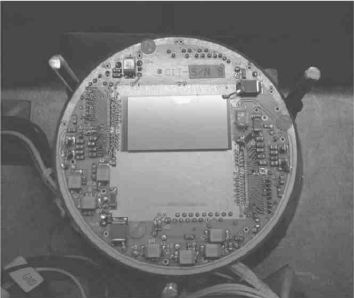
The uniform charge transport properties of the wafer are very important for fabricating large area pixel detectors. The CdTe crystal used here is the THM-CdTe manufactured by ACRORAD[12]. An electrical resistivity of 1109 cm (p-type) is achieved by compensating the native defects with Cl. The grown crystal is large enough to obtain (1 1 1) oriented single crystal wafers with an area as large as 25 25 mm2. We have demonstrated that the wafer shows very good uniformity when we make a large area CdTe detector with planar electrodes[13, 14]. As determined by the measurements with a large planar detector (21 21 mm2 ) by using a collimated -ray beam from an 241Am source, the location of the peak in the pulse height distribution agrees to within 0.1 % and the variation of the area of the 60 keV peak is less than 0.9 %, regardless of the position.
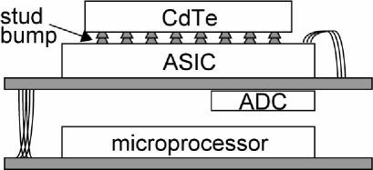
A schematic drawing of the detector is shown in Fig. 2. The detector consists of a CdTe wafer, a front-end ASIC and the data handling circuit including an ADC and a CPU. Charge signals from the individual pixel electrode are fed into the readout circuit built in the ASIC. The ASIC is originally developed by the Caltech group for a CZT pixel detector and features very low noise by means of a capacitor array [17]. The power consumption of the ASIC is as low as 50 W/pixel.
Before assembling the detector, a CdTe wafer with dimensions of 23.7 13.0 mm2 and a thickness of 0.5 mm is prepared. By using polished wafers with (1 1 1) orientation, Pt electrodes are formed by electroless plating for both the common electrode (cathode) and pixel electrodes (anode). The size of each pixel electrode is 448 m 448 m with a gap of 52 m. No control electrode is adopted between electrodes. A guard with 1 mm width surrounds the 24 44 pixels anode pixels.
One of the most difficult parts to realize a fine pitch (finer than several hundred microns) CdTe and/or CZT pixel detectors is to establish a simple and robust connection technology for these fragile devices. High compression and/or high ambient temperature would damage the crystal. Also the co-planarity of the CdTe wafer is measured to be 2 m at most, which is much worse than that of usual silicon wafers. Usual indium-ball soldering might not be appropriate for this purpose. Also indium is easily oxidizable, and needs flux which could contaminate the detector surface. Recently, we have developed indium and gold (In/Au) stud-bump bonding technology, optimized for CdTe detectors, with Mitsubishi Heavy Industries (MHI) in Japan. By following the prescription given in Takahashi et al. [18], but with a slightly modified bump condition, we connected the CdTe wafer to the ASIC. In order to minimize the effect of incomplete charge collection, we apply a negative bias on the common electrode. After we assembled the detector, we have confirmed the connection of 1055 pixels out of 1056 pixels. There is one bad pixel which shows very high noise, regardless of any conditions, such as bias voltage, and temperature. Currently, we do not understand whether the read out circuit is broken, or the bump is not connected for this particular pixel.
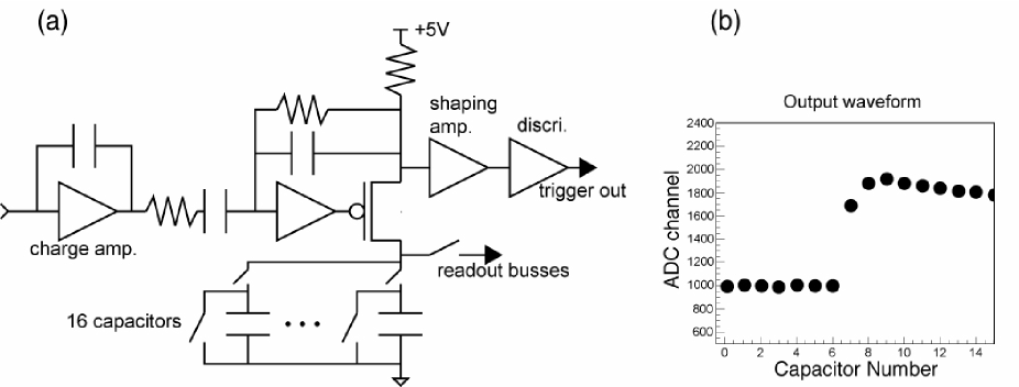
In the ASIC (Fig. 3 (a)), output signal from the preamplifier is continuously integrated by one capacitor to the next with a time interval of 1 s. After a trigger signal is issued from a comparator, the switching sequence continues for the next eight capacitors and then the sequence is freezed for the subsequent readout. The charge in sixteen capacitors is sequentially read out as voltage and converted by the external ADC. Figure 3 (b) shows an example of the output signal for one pixel. Pulse height information for each X-ray photon is calculated by analyzing the recorded pulse shape by the filter algorithm implemented in DSP or by software. The ASIC also reads out data from the surrounding eight pixels together with the data from the triggered pixel. A detailed description of the ASIC is given in Chen et al[17]. For the detector used in this experiment, triggers from five pixels are turned off, because these channels show rather high noise as compared to other channels. The typical noise level is about 50 ADC channel for normal pixels, while the noise level of bad channels is larger than 200 ADC channel. From hereafter, we analyze spectra from 1051 pixels out of total 1056 pixels. At 20 ∘C, the FWHM of the peak measured by the test pulse ranges from 0.4 keV to 0.6 keV when the bias voltage is not applied. This corresponds to the electronic noise of 40 – 60 (RMS).
The spectrum from each pixel is constructed from the pulse height information associated with the trigger. There are two types of events; 1) single-pixel events in which the pulse height of pixels surrounding the triggered pixel is comparable with the noise level, and 2) multi-pixel events in which the energy deposited in the CdTe detector is shared with multiple pixels.
3 Signal Processing and Spectral Analysis
In order to study the spectral performance of the CdTe pixel detector, we start from the search for the optimum operating condition and the investigation of the response from a single pixel. The overall performance, including the pixel by pixel variation will be discussed in the next section.
As the first demonstration of the operation of the CdTe pixel detector, Fig. 4 shows 241Am spectra taken at 20 ∘C and ∘C. Single-pixel events are used to make the spectra. Energy resolutions better than 1 keV (FWHM) are obtained for -ray lines from 14 keV to 60 keV in the spectra. The best resolution is obtained when the detector is operated at the lowest temperature, 50 ∘C. With a bias voltage of 100V, the energy resolution at 14 keV and 60 keV is 0.67 keV and 0.89 keV, respectively. The improvement in the spectral resolution is due to the reduction of the leakage current. At 20 ∘C, the leakage current is estimated to be an order of 10 pA per pixel at –100 V, which is calculated from the results obtained with a planar detector with Pt/CdTe/Pt electrode configuration. Although we need to perform more quantitative measurements, the leakage current at –50 ∘C is expected to be reduced by almost an order of magnitude as compared to that at –20 ∘C.
Charge collection efficiency (CCE) is an important issue for CdTe and CZT, because electrons and holes generated in these semiconductor have low mobility and a short life-time[19]. The low CCE results in the tail-like structure below the peak in the spectrum, which is actually seen in the 241Am spectra (Fig. 4). We study the CCE quantitatively by measuring the 57Co spectrum at different bias voltages under an operating temperature of 50 ∘C. As clearly shown in the case of the 40 V operation (Fig. 7), a significant amount of charge loss is seen as a low-energy tail of the 122 keV line. As the bias voltage is increased to 300 V, a sharp 122 keV peak is obtained. A higher bias voltage is better in terms of the CCE because the fraction of electrons and holes that reach the electrodes increases. However, high bias voltage deteriorates the spectral resolution due to the increase of the leakage current. In the measurements, the best energy resolution for the 14 keV line is obtained at 40V. On the other hand, the best energy resolution of 1.47 keV for the 122 keV line is obtained at 300 V. This is because most of the 14 keV photons interact close to the cathode electrodes, and because the transit of electrons, which is less affected by charge loss, becomes responsible for the pulse height. As an optimum value, we use 300 V as the standard bias voltage from here after.


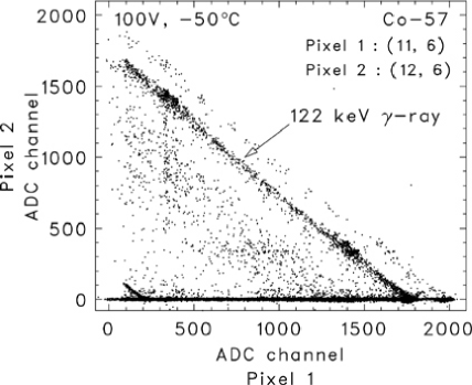

Since the pixel size is as small as 500 m for the CdTe pixel detector, we need to investigate the charge splitting among the adjacent pixels (multi-pixel event). Figure 7 shows a correlation of pulse heights between a triggering pixel and one of the adjacent pixels. It is shown that the energy deposition, corresponds to the 122 keV -ray, is shared between two pixels, for some fraction. Figure 7 compares spectra for single-pixel and multi-pixel events. It is clearly shown that the amount of the tail component is more pronounced when we include multi-pixel events. This implies that the selection of single-pixel events is important to obtain “tail-less” spectra in the CdTe pixel detector.
Long-term stability is an important issue for CdTe and CZT semiconductors [18]. As discussed in our previous publication[13], a CdTe detector with Pt electrode for both cathode and anode sides (Pt/CdTe/Pt) shows good stability. We do not see any spectral degradation for a long term operation of a week or more. In order to verify this with the CdTe pixel detector, we operate it for seven days at an operating temperature of –50 ∘C under a bias of 300 V. An 241Am source is placed above the detector during the measurement. Figure 8 shows the spectra taken at the first day, 1 day later, and 7 days later. No degradation can be observed in the peak positions and the energy resolution. The location of the peak in the pulse height distribution agrees to within 0.2% . The energy resolutions (FWHM) agree within statistical errors. The detector also shows a stable spectral performance at –20 ∘C over one week.

4 Uniformity of the Detector
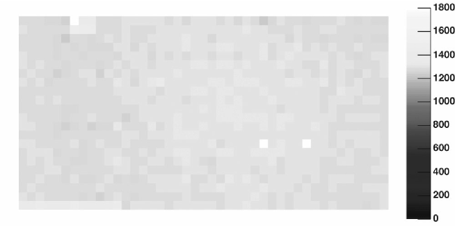


Evaluating the detector uniformity response is an important objective of this experiment. We analyze the uniformity of the detector in terms of spectral properties such as the peak position and the spectral resolution, as well as the detection efficiency.
The location of the peak in the spectrum for mono-energetic -rays has a strong correlation with the charge transport properties of the material[19, 10], especially for electrons. If the mobility-lifetime product is not uniform in the wafer used in the detector, the peak position changes with the pixel location, since we apply a single bias voltage over the entire detector plane. The variations of the size of low-energy tail is explained if the transport properties for holes have some spatial distribution. These spatial variations of charge transport properties could be introduced if the crystal is not uniformly grown.
We study the uniformity by irradiating with an 241Am source from 40 cm above the detector, and obtain flat illumination data. The detector is operated under a bias of 300 V, at a temperature of ∘C. In order to evaluate the charge transport properties, the analog gains for each pixel are calibrated by the using the on-chip test pulse. The average gain variation is 2.8 %, consistent with the number reported in Harrison et al[20]. Figure 11 shows the spatial distribution of the peak position in ADC channel after the gain of readout circuit in the ASIC is calibrated. Distribution of the peak position is almost flat and shows a standard deviation of 0.82 % (Fig. 11), which agrees with the result from the scanning experiment of a planar CdTe detector [18, 14]. Distribution of the energy resolution is also presented in Fig. 11. The average energy resolution is 1.04 keV, and the standard deviation is 0.10 keV.

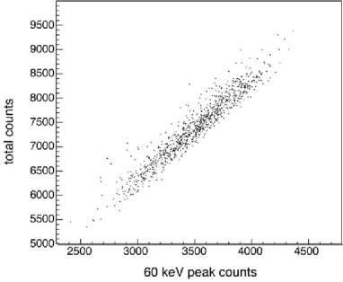



The variation of the count rate is also an important aspect for the pixel detector, since it reflects the variations of the detection efficiency in the detector. In order to produce precise-spectroscopic images, the flat efficiency in the detector plane is desirable to reduce the systematic errors. The uniformity of charge transport properties is again important here. This is because the pixel-to-pixel variation of the fraction of low energy tail affects the flatness of the image when we specify the energy band. Distribution of the area for the 60 keV peak is plotted in Fig. 14. The area is calculated by integrating counts from 45 keV to 65 keV. The variation of the distribution is 8.9 %, which is larger than the statistical variation of 1.1 %. This result is inconsistent with the result for the planar CdTe detector [18, 14].
In order to investigate the reason for the variation of the area, we compare the counts in the 60 keV peak and the total count, and obtain a scatter plot (Fig. 14). From the figure, a strong correlation between the two values is observed. In Fig. 14, we compared the actual spectra of the pixels with the highest and the lowest count at 60 keV. Although the counts are different, the shape of the spectra is very similar. This similarity implies that the variation of the peak area or the total count rate is not caused by the spatial inhomogeneity of charge transport properties, such as mobility and lifetime. This variation then could be explained by two possibilities. One is a reduction of the effective area caused by the bump bonding process. The other is the dead time variations due to the algorithm currently installed in the data acquisition (DAQ) system. We will study this issue more.
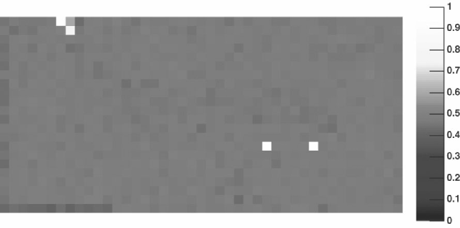
If we assume that the variation of total counts is due to the dead-time variations for each pixel, we can use it as an indicator of the actual integration time for each pixel. Figure 16 shows a map of the “normalized” area (area ratio). In the figure, the integrated counts from 45 keV to 65 keV are normalized by the total counts of the spectrum for each pixel. The resultant variation of the area ratio is 2.1 % while the statistical error is 1.3 %.
5 Imaging Spectroscopy
We perform imaging measurements to demonstrate the performance of imaging spectroscopy. An image mask, made of brass covered with gold, is mounted 6 mm above the detector. It has a length of 70 mm and a thickness of 0.8 mm. The area marked in Fig. 17 (a) is used for the measurement. 241Am and 57Co are located 40 cm above the detector so that the shadow image is obtained with the CdTe pixel detector. The detector is operated at –20 ∘C and 80 V for the pixel is applied.
As shown in Fig. 17 (b) and (c), we have succeeded in imaging spectroscopy using the detector. Fig. 17 (b) is drawn by 13 keV - 26 keV lines from 241Am, while Fig. 17 (c) is by 122 keV line from 57Co. The spoke feature of the mask, which is the same as the pixel size of 500 m, is clearly resolved while a featureless image is obtained for the image selected from the 105 – 130 keV energy band. This result is consistent with the fact that the mask is transparent above 100 keV.

6 SUMMARY
We have developed a large CdTe pixel detector by utilizing recent technologies of an uniform CdTe single crystal, the two-dimensional ASIC, and the In/Au stud bump bonding. When the detector is operated at a temperature of –50 ∘C, the energy resolution (FWHM) for the 14 keV and 60 keV -rays is 0.67 keV and 0.89 keV, respectively. The voltage scanning measurement shows that 10 % of the total event become multi-pixel events, which contributes to the tail structure in thespectra obtained. The detector shows high uniformity as well as the spectral and imaging performances. The location of the peak agrees to within 0.82 % after the analog gain is calibrated by pulser data, and the average energy resolution is 1.04 keV. The variation of the 60 keV peak counts is found to be 8.9 %, which is inconsistent with the result for the planar CdTe detector. Although the reason for this variation is still under investigation, if we assume a “normalized” area, the resultant variation is 2.1 %. In the demonstration of imaging spectroscopy, the detector resolves a 0.5 mm wide line, which is the same as the positional resolution.
Acknowledgements.
The authors would like to thank M. Onishi for his dedicated help throughout the detector development.References
- [1] K. Yamashita, et al., “Supermirror hard-x-ray telescope,” Applied Optics, vol. 37, pp. 8067-8073, 1998
- [2] T. Takahashi, K. Makishima, F. Fukazawa, M. Kokubun, K. Nakazawa, M. Nomachi, H. Tajima, M. Tashiro, and Y. Terada, “Hard X-ray and Gamma-ray detectors for the next mission,”, New Astronomy Reviews, vol 48, pp. 309-313, 2004
- [3] H. Kunieda, “Hard X-ray Telescope Mission (NeXT),” Proc. SPIE, vol. 5488, in press, 2004
- [4] F. A. Harrison, et al., “Technology development for the Constellation-X hard-x-ray telescope,” in Proc. SPIE, vol. 3765, pp. 104-111, 1999
- [5] W. Craig, et al., “NuSTAR,” in Proc. SPIE, vol 5488, in press, 2004
- [6] NeXT Satellite Proposal,the NeXT working group, submitted to ISAS, 2003.
- [7] Y. Ogasaka, K. Tamura, R. Shibata, A. Furuzawa, T. Okajima, K. Yamashita, Y. Tawara, H. Kunieda, “NeXT Hard X-ray Telescope,” Proc. SPIE, vol. 5488, in press, 2004
- [8] T. Takahashi, et al., “Wide-band X-ray Imager (WXI) and Soft Gamma-ray Detector (SGD) for the NeXT mission,” Proc. SPIE, vol. 5488, 2004
- [9] F. A. Harrison, S. E. Boggs, A. E. Bolotnikov, C. M. H. Chen, W. R. Cook and S. M. Schindler, “Development of CdZnTe pixel detectors for astrophysical applications”, Proc. SPIE, vol. 4141, pp. 137-143, 2000
- [10] G. Sato, T. Takahashi, M. Sugiho, M. Kouda, T. Mitani, K. Nakazawa, Y. Okada, and S. Watanabe, “Characterization of CdTe/CdZnTe detectors,” IEEE Trans. Nucl. Sci., vol 49, No. 3, pp. 1258-1263, 2002
- [11] M. Suzuki, et al. “Hard X-ray Response of CdZnTe Detectors in the Swift Burst Alert Telescope,” IEEE Trans. Nucl. Sci., in print, 2003
- [12] M. Funaki, et al., “Growth and Characterization of CdTe Single Crystal for Radiation Detectors,” Nucl. Instrum. Methods., vol. A436, pp. 120-126, 1999
- [13] T. Takahashi, T. Mitani, Y. Kobayashi, M. Kouda, G. Sato, S. Watanabe, K. Nakazawa, Y. Okada, M. Funaki, R. Ohno, and K. Mori, “High Resolution Schottky CdTe Diodes,” IEEE Trans. Nucl. Sci., 49, No. 3, pp. 1297-1303, 2002
- [14] K. Nakazawa, T. Takahashi, S. Watanabe, G. Sato, M. Kouda, Y. Okada, T. Mitani, Y. Kobayashi, Y. Kuroda, M. onishi, R. Ohno, and A. Kitajima, “Large-area CdTe diode detector for space application,” Nucl. Instrum. Methods, vol. A512, pp. 412-418, 2003
- [15] T. Mitani, T. Tanaka, K. Nakazawa, T. Takahashi, T. Takashima, H. Tajima, H. Nakamura, M. Nomachi, T. Nakamoto, Y. Fukazawa “A Prototype Si/CdTe Compton Camera and the Polarization Measurement”, IEEE Trans. Nucl. Sci., in press, 2004
- [16] T. Tanaka et al.,“Development of a Si/CdTe semiconductor Compton Telescope,” Proc. SPIE, vol. 5501, in press, 2004
- [17] C. M. H. Chen, et al. “Characterization of the HEFT CdZnTe pixel detectors,” Proc. SPIE, vol. 5198, pp. 9-18, 2003
- [18] T. Takahashi, et al., “High-Resolution CdTe Detector and Applications to Imaging Devices”, IEEE Trans. Nucl. Sci., 48, pp. 287-291, 2001
- [19] T. Takahashi and S. Watanabe “Recent Progress on CdTe and CdZnTe detectors,” IEEE Trans. Nucl. Sci., vol. 48, pp. 950-959, 2001
- [20] F. Harrison, et al., “Development of a high spectral resolution cadmium zinc telluride pixel detector for astrophysical applications,” Proc. SPIE, vol 4851, pp. 823-830, 2003