Send offprint requests to: P. Schuller, e-mail: pschuller@cfa.harvard.edu
LLiST - a new star tracker camera for tip-tilt correction at IOTA 111 Copyright 2004 Society of Photo-Optical Instrumentation Engineers (SPIE). This paper was (will be) published in New Frontiers in Stellar Interferometry, W. A. Traub, ed., SPIE Proceedings Series, Vol. 5491, paper [5491-126]. and is made available as an electronic reprint (preprint) with permission of SPIE. One print or electronic copy may be made for personal use only. Systematic or multiple reproduction, distribution to multiple locations via electronic or other means, duplication of any material in this paper for a fee or for commercial purposes, or modification of the content of the paper are prohibited.
Abstract
The tip-tilt correction system at the Infrared Optical Telescope Array (IOTA) has been upgraded with a new star tracker camera. The camera features a backside-illuminated CCD chip offering doubled overall quantum efficiency and a four times higher system gain compared to the previous system. Tests carried out to characterize the new system showed a higher system gain with a lower read-out noise electron level. Shorter read-out cycle times now allow to compensate tip-tilt fluctuations so that their error imposed on visibility measurements becomes comparable to, and even smaller than, that of higher-order aberrations.
keywords:
interferometry, tip-tilt correction1 INTRODUCTION
The Infrared Optical Telescope Array (IOTA) is located at the Smithsonian Institution’s Whipple Observatory on Mount Hopkins, Arizona[(1)]. It operates with three telescopes and offers multiple baselines in the range 5 to . Typical site conditions, observed at the MMT Observatory[(2)] with a central wavelength , show a median seeing (FWHM) and a median (ground) wind speed . Both these numbers can become at least 2 times larger. They also allow the derivation[(3), (4)] of the Fried parameter and the coherence time which can be interpreted as scale length and time over which the phase fluctuations of a light wavefront coming from a star and entering the telescope aperture may be considered as sufficiently small. In a crude approximation, and (assuming dominance of ground wind speed), which yields and . In the H band, in which the IONIC fiber beam combiner at IOTA operates[(5), (6)], and using the fact that , so that and . The telescopes at IOTA have an entrance pupil which is of the same order of magnitude as . Therefore, tip-tilt correction of the incoming beam compensates for atmospherically induced aberrations already to a high degree[(7), (8)] where remaining visibility errors are dominated by higher-order aberrations.
The overall procedure for tip-tilt correction that is applied at IOTA for each of the three telescopes is as follows. The visible parts of the beams are focused onto a CCD, i. e., one CCD frame shows three individual star images. The positions of the centroids are retrieved and compared to the nominal positions. Then the tertiary mirrors, which are mounted on 2-axis piezo driven stages, are adjusted accordingly. The whole process aims at stabilizing the infrared star image on the fiber input of the interferometer. Movements due to residual tip-tilt errors are reflected in varying flux recorded in the interferometer outputs.
As the aforementioned and more detailed considerations[(9), (10)] indicate, the goal is therefore to apply tip-tilt correction with an overall cycle time and as short as . An important unit in the tip-tilt correction system is the star tracker CCD camera. Its sensitivity, read-out frame rate, and read-out noise majorly determine if this goal can be achieved. Previously, the camera in use at IOTA could reach frame rates of , which is a factor of 5 slower than the envisaged goal, and it would allow tracking stars with an apparent magnitude of up to , depending on integration time and seeing conditions. Recently, IOTA acquired a new CCD camera in order to reach full tip-tilt correction. In the following sections, we present first test results of this new camera.
2 CAMERA PROPERTIES
The new star tracker camera for IOTA was acquired from MIT Lincoln Laboratory (LL) - hence the acronym LLiST. Its design is based on an imager already developed for adaptive optics applications[(11), (12)]. Figure 1 shows the overall setup of LLiST as it is implemented at IOTA.
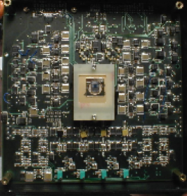
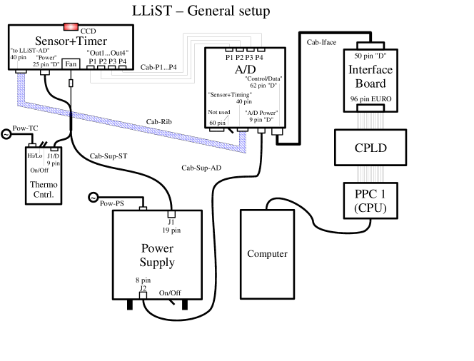
The CCD is kept in a sealed housing, cooled by a thermo-electric cooler (TEC) and mounted on the so-called sensor board. The timing board, which is mounted together with the sensor board in one case, controls the clocking of the analog and digital data and provides synchronization signals for the IOTA control system[(13)]. A programmable logic device (CPLD) controls the camera[(14)], receives data from it, and transfers data for further processing.
2.1 Chip characteristics
The central part of LLiST is a -pixel backside-illuminated CCD. Figure 2 shows the spectral response of the chip showing a maximum of 90% near .

A pixel is on a side, with a full well capacity of about 175,000 electrons. The fill factor of the chip is close to .
At IOTA, the telescope beams are first compressed by a factor of 10 to a diameter and then focused on the ST camera by means of lenses with focal length . This yields a pixel scale on the sky of . The effective full field of view (FOV) on the sky is per telescope, constrained by the optical train of the instrument. Assuming the diffraction limited case (Airy pattern), the central lobe of the star image on the CCD has a diameter , a little over one pixel.
2.2 Read-out process
The area of the CCD exposed to light is sub-divided in four ports. Each port has its own analog and digital amplifier chain. An exposed frame is first transfered to a storage area protected from light and is then read out sequentially row by row into serial registers which are transfered to separate amplifier chains. In addition to receiving and transfering charge from the exposed frame, a serial register contains four physical pixels which are also shielded from light exposure. For this reason, and because of their short idle time (; see clocking rate below) during read-out, these pixels can be used in principle as reference for the chip bias. When digitizing data on the analog-to-digital (AD) board, the order of pixels is re-arranged so that the reference pixels of all four ports come out last in a row.
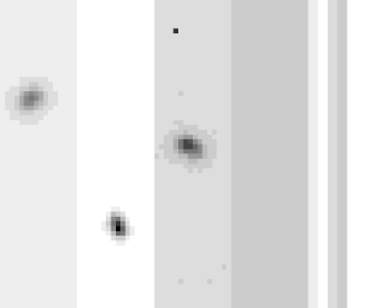
The camera offers a number of different read-out modes of which to date mainly two have been in use. In Mode 1 (M1) the full frame is read out unbinned, whereas Mode 2 (M2) bins pixels during the read-out process. Clocking rates of the serial register are for M1 and for M2. Maximum possible read-out frame rates on the camera side are frames per second (fps) in M1 and in M2, whereas observed cycle times of the control software with open star tracker control loop were and , respectively. The limiting factor here is the data handling in the control software, a matter currently being worked on. Figure 3 shows sample frames of M1 and M2, respectively.
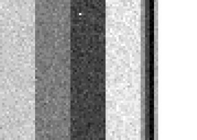

Other modes read out only a window of the full binned mode, i. e., a certain number of rows.
2.3 Amplifier chain
On the sensor board, collected charge is converted by some capacitance into a voltage fed to a pre-amplifier. This step is characterized by the responsivity of the board electronics (=V/e-). It is not known a priori, but can be determined (see Sect. 2.4). The signal is pre-amplified with an electronic gain , whereby the dynamic output range of the pre-amplifier in LLiST is . A 14-bit AD converter transfers this analog signal into analog-to-digital units (ADU), having a conversion factor with . The overall behavior of the entire system is characterized by the system gain ( e-/ADU) with
| (1) |
2.4 Read-out noise and system gain
2.4.1 Mode 1
To determine the read-out noise (RON) standard deviation and the system gain in Mode 1, we applied a variant of the photon-transfer technique as outlined in Ref. 16. It uses the relation between the overall standard deviation of the number of electrons collected in a pixel, the standard deviation due to photo-electron and dark current noise, and in (e- RMS):
| (2) |
This relation is converted by the camera system into ADUs through its system gain :
| (4) |
In the second to last step we inserted the signal value for its variance , assuming Poisson statistics for thermally generated and photo-electrons. Equation 4 describes a linear relation between the measured signal and the total measured variance , whereby the slope represents the inverse of the system gain and the intercept the squared product of and the read-out noise , which can also be interpreted as remaining noise at zero light level.
Assuming that all pixels on the CCD basically behave the same way (i.e., common system gain ) and follow the same statistics, one can expose the CCD to a non-uniform light distribution and take a number () of frames sufficiently high to derive statistical values from them. For each pixel, the signal and noise values will create a data point. The set of data points will scatter around the linear relation (4) so that linear regression can be applied.
Figure 4 shows some results of this procedure. For the necessary subtraction of the camera bias, the reference pixels were averaged to one number which was subtracted off its corresponding port. Dark current was not subtracted, but treated as part of the signal. The linear fit was done at comparatively low signal levels with a higher data point population and where read-out noise becomes important.


2.4.2 Mode 2
For Mode 2, we had to apply a method slightly extended from the one used for Mode 1. Due to camera-internal reasons, the reference pixels in Mode 2 are not good indicators of the bias, they carry erroneous signal. Moreover, due to the binning, the number of pixels is strongly reduced and therefore application of the photon-transfer technique would show scarce population along the regression line. Furthermore, it was not clear from the beginning how low the CCD had to be cooled so that dark current noise would not affect operation with intended integration times up to 100 .
For these reasons we rather took a series of dark frames with increasing and treated the thermally induced dark current as signal. This signal is plotted versus and a linear regression is performed. The intercept of the ordinate yields the bias (“signal at zero integration time”) whereas the slope in this plot yields the dark current:
| (5) |
The bias was subtracted off all frames. These frames were then used to perform a reduction similar to the one described in the previous section for Mode 1. For Mode 2, pixel values and signal variances were averaged over a port to create one data point for a given integration time.
This method was first applied to dark frames taken in Mode 1 to verify validity and confirm the results found by the photon-transfer technique. Some results obtained for Mode 2, at the lowest temperature possible with the current setup (C), are shown in Figure 5.


They show that the system gain in Mode 2 is the same as in Mode 1, yet the read-out noise is roughly a factor 2 higher. In both modes the read-out noise corresponds to more than 2 bits of the AD converter, which is not optimal since this restrains its dynamic range. Also, the signal increases with integration time stronger than expected from the linear fit performed at lower signal levels. Non-linearity is roughly 9% at . The reason for this behavior is not yet clear and under investigation. In any case, this fact should have an only marginal effect on the operation.
Figure 6 shows a compilation of the dark current obtained at different temperatures for Mode 1 and Mode 2 and an exponential fit to them.


The line at the bottom of the plots indicates the level where the photon noise originating from dark current at an integration time equals the read-out noise in the respective mode. It becomes apparent that it is necessary to cool down to C. This task will be addressed in the near future at IOTA by attaching the fluid circuit of a glycol/water chiller to the heat sink of the CCD housing. The water chiller can reach temperatures of about C. This allows the thermo-electric cooler to pump heat against a heat sink roughly C lower than currently room temperature and, therefore, reach the envisaged temperature.
3 SUMMARY
The new CCD camera for the star tracker system at IOTA was installed earlier this year (2004) and has satisfactorily performed since. A summary of characteristics is given in Table 1.
| LLiST: CCD back illuminated | Previous camera: | ||
|---|---|---|---|
| Mode 1 | Mode 2 | CCD front illuminated | |
| (unbinned) | ( binned) | ( binned) | |
| Pixel size | 21 | 84 | |
| Frame size | |||
| Pixel scale on sky | 0.72 | 2.9 | |
| Full FOV on sky (unvignetted) | |||
| Central spot of diffraction | |||
| limited star image at | |||
| Maximum quantum efficiency | 90% at | 40% at 0.6 | |
| Optical uniformity | |||
| Full well capacity | 175,000 e- | ||
| Fill factor | |||
| Pixel clock-out rate | 1.1 | 0.25 | |
| Maximum frame rate | 796 | 2220 | 200 |
| Electronic gain | |||
| of pre-amplifier | 6.8 | ||
| AD converter | 2.5 on 14 bit | ||
| System gain | e-/ADU = e-/ADU | e-/ADU | |
| Responsivity | |||
| on CCD | |||
| RON (rms) | e- | e- | e- |
| ADU | ADU | ADU | |
| Linearity up to | |||
| Dark current at | |||
| (1 bright pixel) | e-/ms | e-/ms | |
| Limiting magnitude | ?? [improvement by expected] | ||
The overall quantum efficiency of the CCD doubled, the frame rate of the camera increased by a factor 4 to 5 up to the desired frame rate, the system gain improved by a factor 4, and read-out noise electrons were reduced by nearly a third operating in the unbinned Mode 1. Furthermore, first experience on the sky show an increase in sensitivity of roughly 1 , depending on spectral type of the star. Remaining issues are to be resolved: reducing high dark current to a non-disturbing level by additional cooling measures; lowering increased read-out noise in the binned Mode 2; balancing system gain and read-out noise for optimal use of the dynamic range of the AD converter. These tasks are expected to be accomplished in the summer down time before the start of the observing season in fall 2004. Other issues like the optimization of the IOTA system control software for the fast frame rates of LLiST will be addressed in the near future.
Acknowledgements.
We thank all members of the Advanced Imaging Technology Group at MIT Lincoln Laboratory for their support under the leadership of Dr. Bernard B. Kosicki.The reported work was funded by the US National Science Foundation (NSF) under grant number AST-0138303 to F. P. Schloerb (PI) at University of Massachusetts.
This publication made use of NASA’s Astrophysics Data System (ADS) Abstract Service (http://adsabs.harvard.edu/).
References
- (1) W. A. Traub et al., “IOTA: recent technology and science,” in New Frontiers in Stellar Interferometry, W. A. Traub, ed., SPIE Proceedings Series 5491, 2004. (these proceedings).
- (2) D. Blanco, “MMT Seeing,” 2003. URL http://www.mmto.org/~dblanco/Seeing_Stats/MMT_Seeing.pdf.
- (3) A. Glindemann, S. Hippler, T. Berkefeld, and W. Hackenberg, “Adaptive Optics on Large Telescopes,” Experimental Astronomy 10, pp. 5–47, Apr. 2000.
- (4) R. K. Tyson, Principles of Adaptive Optics, Academic Press, Boston London, 2nd ed., 1998.
- (5) J. Berger, P. Haguenauer, P. Y. Kern, K. Rousselet-Perraut, F. Malbet, S. Gluck, L. Lagny, I. Schanen-Duport, E. Laurent, A. Delboulbe, E. Tatulli, W. A. Traub, N. Carleton, R. Millan-Gabet, J. D. Monnier, E. Pedretti, and S. Ragland, “An integrated-optics 3-way beam combiner for IOTA,” in Interferometry for Optical Astronomy II, W. A. Traub, ed., SPIE Proceeding Series 4838, pp. 1099–1106, 2003.
- (6) S. Ragland et al., “Characterizing closure-phase measurements at IOTA,” in New Frontiers in Stellar Interferometry, W. A. Traub, ed., SPIE Proceedings Series 5491, 2004. (these proceedings).
- (7) S. Shaklan and F. Roddier, “Coupling starlight into single-mode fiber optics,” Appl. Opt. 27, pp. 2334–2338, 1988.
- (8) T. ten Brummelaar, “The contribution of high order Zernike modes to wavefront tilt,” Optics Communications 115, pp. 417–424, 1995.
- (9) T. ten Brummelaar, J. Hildebrand, and S. Ridgway, “Wobbler Servo Requirements,” Tech. Rep. 19, CHARA Optical Array, 1995. URL http://www.chara.gsu.edu/CHARA/Reports/tr19.ps.
- (10) W. J. Tango and R. Q. Twiss, “Michelson stellar interferometry,” in Progress in Optics, 17, pp. 239–277, North-Holland Publishing Co., Amsterdam, 1980.
- (11) R. K. Reich, R. W. Mountain, W. H. McGonagle, J. C.-M. Huang, J. C. Twichell, B. B. Kosicki, and E. D. Savoye, “Integrated electronic shutter for back-illuminated charge-coupled devices,” IEEE Transactions on Electron Devices 40, pp. 1231–1237, 1993.
- (12) B. E. Burke, J. A. Gregory, A. H. Loomis, C. C. Cook, D. J. Young, M. J. Cooper, T. A. Lind, G. A. Luppino, and J. L. Tonry, “CCD imager technology development at Lincoln Laboratory,” in Optical Detectors for Astronomy II: State-of-the-Art at the Turn of the Millenium, Astrophysics and Space Science Library, pp. 187–199, Kluwer Academic Publisher, 2000.
- (13) F. P. Schloerb et al., “Control system software for the IOTA,” in New Frontiers in Stellar Interferometry, W. A. Traub, ed., SPIE Proceedings Series 5491, 2004. (these proceedings).
- (14) E. Pedretti, R. Millan-Gabet, J. D. Monnier, S. Morel, W. A. Traub, N. P. Carleton, J. Berger, P. Schloerb, M. K. Brewer, S. Ragland, and M. G. Lacasse, “Reconfigurable electronics at the IOTA interferometer,” in Interferometry for Optical Astronomy II, W. A. Traub, ed., SPIE Proceeding Series 4838, pp. 943–955, 2003.
- (15) MIT Lincoln Laboratory, 2004. Lexington, MA, USA.
- (16) J. R. Janesick, K. P. Klaasen, and T. Elliott, “Charge-coupled-device charge-collection efficiency and the photon-transfer technique,” Opt. Eng. 26(10), 1987.