Characterizing IMARAD CZT Detectors with Time Resolved Anode and Cathode Signals
Abstract
We present the results of using standard IMARAD CZT detectors with a 100 MHz readout of the anode and cathode pulses. The detectors, 2 cm x 2 cm large and 0.5 cm thick, have 64 Indium pixellated anode contacts at a pitch of 2.5 mm. We investigate the possibilities to improve on the detector’s photo-peak efficiency and energy resolution using two depth of interaction (DOI) indicators: (i) the total charge induced on the cathode and (ii) the drift time of the electron cloud determined from the anode and/or the cathode pulses. The DOI correction with the cathode charge gives better results, increasing the 662 keV photo-peak efficiency by 57% and improving the energy resolution from 2.33% to 2.15% (FWHM, including the electronic noise). The information on the time dependence of the induced charge can be used as a diagnostic tool to understand the performance of the detector. Detailed comparison of the pulse shapes with detector simulations gives the electron mobility and drift time and makes it possible to assess the weighting potential and electric field inside the detector.
Index Terms:
CZT, IMARAD, Detector SimulationsI Introduction
Cadmium Zinc Telluride (CZT) has emerged as the detector material of choice for X-rays and Gamma-rays because of its large bandgap, excellent spatial and energy resolution, high stopping power, and extremely high photo-effect cross section. We are interested in CZT detectors as focal plane detectors for future space-borne X-ray and Gamma-ray telescopes, such as EXIST (Energetic X-Ray Imaging Survey Telescope) [1] and ACT (Advanced Compton Telescope) [2]. In this paper we report results from testing standard IMARAD detectors with a time resolved readout (Sections 2 and 3). We investigated different options to correct the anode signals for the depth of the primary interaction. A simplified detector model and a comparison of simulated and measured signals are presented in Section 4. A summary and outlook are given in Section 5.
II Equipment
The data presented in these proceedings are for a standard Indium contacted 64 pixel IMARAD CZT detector [3]. Previous measurements of IMARAD detectors have been reported by Li et al. [4], Hong et al. [5] and Narita et al. [6, 7]. The detector dimensions are 2 cm x 2 cm x 0.5 cm with the pixel size being 1.6 mm square at a 2.5 mm pitch. The electronics included 4 channels (3 anode pixels plus the cathode) to read out the pulses with an analog bandwidth of 100 MHz similar to the setup described in [8]. Using fast electronics enabled measurement of the drift time of electrons in the detector to a resolution of 10 ns. In addition, we used a 16 channel ASIC [9], which allows us to measure pulse height information for 16 additional pixels. We plan to use the ASIC readout to study events occurring between pixels. The low noise design of the electronics used batteries for power and batteries for the high-voltage supply, cooled external fets, and ground isolation. The 100 MHz signal from the detector is digitized by a 500 MHz oscilloscope and read into a PC for analysis.
III Measurements
III-A Pulse Shape Analysis
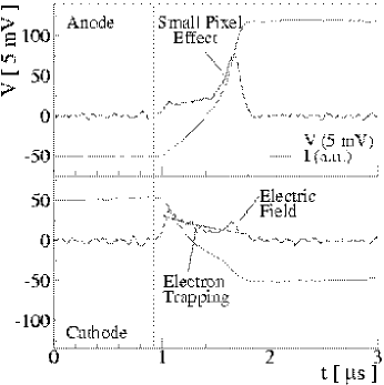
The following measurements were made using a Cs137 source which emits an X-ray line at 662 keV. Figure 1 shows a single pulse induced by a photon interacting with the detector. The CZT is irradiated from the cathode side. While low-energy photons do not penetrate far into the detector, most 662 keV photons do not interact with the CZT; the few interactions are basically homogeneously distributed within the detector volume. The detector is biased at -500 V on the cathode with each of the pixels held at ground. The electrons drift at an almost constant velocity. Shortly before impinging on the pixels, they induce most of the charge. The small pixel effect ([10, 11]) is seen in Figure 1 by a peak in the anode current (dashed line) toward the end of the pulse. The cathode does not show this effect. For many pulses we observed an increase of the cathode current towards the end of the pulse. This increase may correspond to an increased electric field near the anode pixels. However, the effect is not yet fully understood. The electron trapping is seen in an exponential decrease of the current on the cathode.
III-B Cs137 Spectra
From data as shown in Figure 1, we determined the drift time of the electron cloud in the detector, and the amplitudes of the anode and cathode pulses. The drift time is directly correlated with the depth of interaction in the detector ([12, 13]). We used a Cs137 source to produce several thousand events in the detector and read them with a PC.
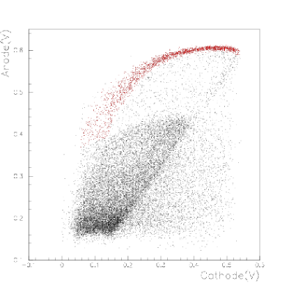

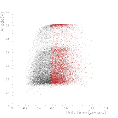

Figure 2 is a plot of the cathode charge versus the charge induced on an anode pixel. 662 keV photo-effect events produce a clearly recognizable arc in Figure 2. A histogram of the anode signals is shown by the solid line in Figure 3. The photo-peak has a FWHM of 2.33%. Correcting the anode signal for the DOI with the cathode signal improves the energy resolution to 2.15% and increases the photopeak efficiency by 57% (see the dashed line in Figure 3). Similar results have been reported by Hong et al. [5]. By subtracting the electronic resolution in quadrature we obtained a pre-correction energy resolution of 1.8% and a post-correction energy resolution of 1.6%.
Figure 4 presents the same data showing the anode amplitude versus the drift time. The photo-peak is obvious but there is no clear correlation of amplitude and drift time which could be used to correct the anode signals for DOI effects. Selecting events with drift times larger than 0.57 -sec, improves the energy resolution from 2.33% to 2.12% (1.5% after subtracting electronic noise) but the photo-peak efficiency decreases by 14% (see Figure 5).
IV Simulations
The simulations are based on a two-dimensional model. The pixel width corresponds to that of the standard IMARAD detector. We chose a slightly larger pixel pitch to mimic the 3-D geometry with our 2-D model. The weighting potential for each pixel and the electric field inside the detector were determined using a commercial semiconductor device simulator package called ATLAS [14]. We modeled the CZT detector with a bulk region and several layers to mimic surface conductivity and contact resistance. The bulk is doped with electrons/cm3 We used surface layers with a higher electron concentration than the bulk to simulate the surface conductivity [15]. We also included significant contact resistance based on pixel-cathode and pixel-pixel I-V measurements. The contact resistivity of individual pixels is on the order of several G. Figure 6 shows a diagram of the model.
The ATLAS simulations give us the weighting potential for all contacts and the electric field under realistic bias conditions. The weighting potentials and electric field were used with our own code to track electrons though the detector and to produce events similar to real ones. The velocity of the electrons is determined by the electric field and the assumed mobility.
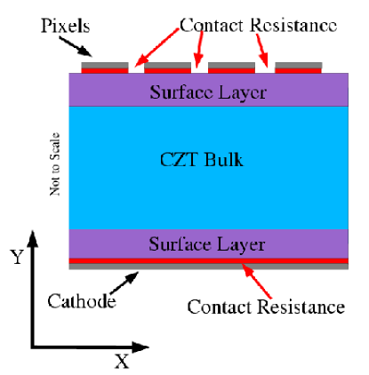
Figure 7 compares a simulated spectrum to the actual data. The mobility and trapping parameters of the simulations were chosen to optimize the agreement between the simulations and the data. The mobility is given directly by the longest drift times while the trapping is constrained by the slope of the photo-peak line (longer drift time events will produce less charge). The simulations deviate from the data in the region of short drift times. We found that these events primarily have interaction sites between pixels (see Figure 8). The results indicate the electric field and/or the weighting potential are not simulated correctly between pixels. Other areas of improvement might include the contact properties and the conductive surface region. Also, an extension from a two-dimensional model to a three-dimensional one will no doubt improve the simulation. Based on these simulations and -sec. Previous studies of IMARAD detectors have shown similar results [4]. The results depend strongly on the assumed contact resistance. Further 3 point measurements of the latter are underway to improve our estimate.
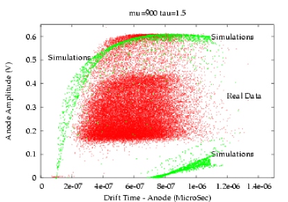
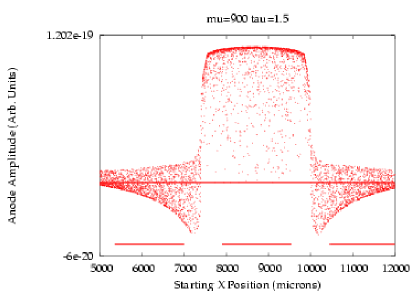
Figure 8 presents the charge induced on the anode versus the initial interaction position. In this figure, the pixels are shown as horizontal lines along the bottom with the pixel under observation being the middle line. This only shows the horizontal interaction position and not the depth of interaction (that can be seen in Figure 7 since there is a direct relation between interaction depth and drift time). The events occurring directly above the pixel induce the most charge while those events occurring off pixel induce less. This indicates there is charge sharing between neighboring pixels which has been seen in other CZT detectors [16]. There are also events occurring above other pixels that induce negative charge on the observed pixel. In the real data, events with low anode charges are masked by the Compton events and are not observed.
V Summary and Outlook
In summary we have made measurements of the photo-peak of a 662 keV Cs137 line using standard Indium contacted IMARAD detectors giving a FWHM of 2.15% (1.6% after subtracting the electronic contribution). These detectors are substantially less expensive than standard high-pressure Bridgman CZT and are thus extremely promising for experiments requiring large detector areas. The correction with the cathode amplitude produces better results than the correction with drift times. Time resolved measurements of events allow for development and fine tuning of simulations which subsequently allows for optimization of new detectors.
Astrophysical applications require CZT detectors with broad energy coverage. However, at photon energies below 100 keV leakage currents deteriorate the performance of IMARAD detectors. Reduced leakage currents have been achieved with Au and Pt contacts ([5, 6]). We next intend to improve on these results by systematically testing high work function metals (Pt, Cr, Ni, etc.) in combination with different surface preparation and passivation methods. The detectors are produced in a class-100 clean room. We use standard photolithographic methods to pattern the anode sides. Results with novel contact and steering grid geometries will be presented in a forthcoming paper.
Acknowledgment
The authors would like to thank Uri El Hanany of IMARAD for supplying us with crystals, Jim Matteson of UCSD for discussing the electronics, and our shop technicians for manufacturing the equipment.
References
- [1] Grindlay, J.E., Craig, W.W., Gehrels, N., et al. 2003, Proceedings of the SPIE, 4851, 331
- [2] Milne, P.A., Kroeger, R.A., Kurfess, J.D., The, L.-S. 2001, astro-ph/0110346
- [3] IMARAD Imaging Systems, Ltd., Rabin Park, 10 Plaut Street, Rehovot, ISRAEL
- [4] Li, W., He, Z., Knoll, G.F., et al. 2001, NIMA, 458, 518
- [5] Hong, J., Bellm, E.C., Grindlay, J.E.,Narita, T. 2003, Proceedings of the SPIE, 5165-06
- [6] Narita, T., Bloser, P., Grindlay, J., Jenkins, J., and Yao, H. 2000, Proceedings of the SPIE 4141, 89
- [7] Narita, T., Bloser, P., Grindlay, J., Jenkins, J., and Yao, H. 1999, Proceedings of the SPIE 3768
- [8] Matteson, J.L., Pelling, M.R., Skelton, R.T. 2002, Proceedings of the SPIE, 4784
- [9] eV Products, 373 Saxonburg Boulevard, Saxonburg, PA 16056
- [10] Barret, H.H., Eskin, J.D., Barber, ,H.B. 1995, Phys. Rev. Lett., 75, ,156
- [11] Luke, P.N. 1995, ,In: Procs. of the “9th International Workshop on Room Temperature Semiconductor X- and Gamma-Ray Detectors, Associated Electronics and Applications”, Grenoble, France, 18-22 Sept., 1995
- [12] Kalemci, E., Matteson, J.L. 2002, NIMA, 478, 527
- [13] He, Z., Li, W., Knoll, G.F., et al. 1999, NIMA, 422, 173
- [14] SILVACO International, Inc., 4701 Patrick Henry Drive, Building 2, Santa Clara, CA 95054
- [15] Bolotnikov, A.E., Chen, C.M.H., Cook, W.R., et al. 2002, IEEE Transactions on Nuclear Science, 49, 1941
- [16] Bolotnikov, A.E., Cook, W.R., Harrison, F.A., et al. 1999, NIMA, 432, 326