Modeling Charge Transfer Inefficiency in the Chandra Advanced CCD Imaging Spectrometer
Abstract
The front-illuminated (FI) CCDs in the Advanced CCD Imaging Spectrometer (ACIS) on the Chandra X-ray Observatory (Chandra) were damaged in the extreme environment of the Earth’s radiation belts, causing charge traps that result in enhanced charge transfer inefficiency (CTI) during parallel readout. This causes row-dependent gain, event grade ‘morphing’ (spatial redistribution of charge) and energy resolution degradation.
The ACIS back-illuminated (BI) CCDs also exhibit pronounced CTI due to their manufacturing. It is mild enough that position-dependent energy resolution is not seen, but it is present in both parallel and serial registers. This CTI also changes the gain and event grades, in a spatially complicated way as parallel and serial CTI interact.
Given these realities, we have developed and tuned a phenomenological model of CTI for both FI and BI CCDs and incorporated it into our Monte Carlo simulations of the ACIS CCDs. It models charge loss and the spatial redistribution of charge (trailing), thus reproducing the spatially-dependent gain and grade distribution seen in all ACIS CCDs and the row-dependent energy resolution seen in the FI devices. Here we explore the evidence for CTI, compare our simulations to data, and present a technique for CTI correction based on forward modeling.
keywords:
CCD , charge transfer inefficiency , Monte Carlo simulationPACS:
95.55.Ka , 95.75.Pq , 02.70.Lq , 07.05.Tp, , , and
1 Introduction
This paper is the third in a suite of articles outlining recent efforts to improve the modeling of CCDs used in the Chandra X-ray Observatory (hereafter Chandra). The Advanced CCD Imaging Spectrometer (ACIS) instrument employs bulk front-illuminated (FI) CCDs and back-illuminated (BI) CCDs to give good spectral resolution and good 0.2–10 keV quantum efficiency [1]. These devices, designed and manufactured at MIT’s Lincoln Laboratories [2], couple with the Chandra mirrors to give users the ability to do spatially-resolved X-ray spectroscopy on spatial scales comparable to ground-based visual astronomy.
In the first paper in this series [3], Pavlov and Nousek developed a solution to the diffusion equation, including recombination, to describe the process of charge diffusion in field-free regions of CCDs. In the second paper ([4], hereafter T01), Townsley et al. describe the latest Pennsylvania State University (PSU) CCD simulator, which includes the results from Pavlov and Nousek and many recent innovations in CCD modeling made by our ACIS team colleagues at the Massachusetts Institute of Technology (MIT) Center for Space Research (CSR) [5], [6], [7]. T01 also gives introductory material such as the geometry of ACIS devices and the event grading scheme used; readers unfamiliar with the operation of X-ray CCD cameras should see that paper and references therein for details. This paper narrows the focus of T01 to a calibration complication with the ACIS CCDs – charge transfer inefficiency (CTI).
Below we discuss the pronounced CTI effects observed in ACIS flight data. CTI is a phenomenon in which some of the charge resulting from an X-ray photon’s interaction with the CCD is lost as that charge is transferred across the device to the readout nodes. Thus CTI changes the gain across the device. It also causes spatial redistribution of the charge in the pixel neighborhood of an event, as charge traps capture electrons and release them on short timescales during the readout process. This results in charge being redistributed in surrounding pixels within the region recognized as a single event. Charge loss can be substantial (equivalent to the reduction of apparent X-ray energy of over 100 eV), depending on photon energy and the event’s position with respect to the CCD readout nodes.
Due to the unanticipated forward scattering of charged particles (probably mainly 100 keV protons [8], [9]) by the Chandra mirrors onto the ACIS CCDs, the FI devices suffered degraded performance on-orbit, most pronounced at the top of the devices, near the aimpoint of the imaging array. This radiation damage created charge traps with a variety of time constants that increased the parallel CTI of these devices markedly, resulting in the equivalent of several years of damage in only a few weeks of operation.
As a result of their manufacturing process, the ACIS BI devices have always shown modest serial and parallel CTI effects, but their geometry has protected them from severe radiation damage on-orbit so they show no additional CTI. Although operational changes have halted the rapid degradation of the FI devices, the space environment is likely to increase CTI effects slowly on all chips throughout the life of the mission. Prior to launch we began development of a CTI model for BI devices and a data correction process to remove CTI effects. We have extended this model and corrector to address both BI and FI CTI effects at two operating temperatures.
To ensure that no water ice could collect on Chandra’s instruments, the focal plane temperature of the Observatory was kept at the relatively warm setting of 110C from mid-September 1999 to the end of January 2000. Thereafter, it was determined that the Observatory structures had outgassed enough that it was safe to lower the focal plane temperature to 120C. At this new colder temperature, the trap population that causes the row-dependent energy resolution in FI devices is partly suppressed [9], [10]. This step greatly improved the performance of the FI devices by ameliorating the effects of CTI. The BI CTI is very slightly worse at 120C than at 110C but the improvements in the FI performance completely justify operating at 120C.
Given the existing and potential complication CTI causes for ACIS calibration, we have developed a model for CTI and incorporated it into our Monte Carlo CCD simulator. CTI is parameterized as a function of the charge in each pixel, including the effects of de-trapping (charge trailing), shielding within an event (charge in the leading pixels of the 33 pixel event island protect the rest of the island by filling traps), and non-uniform spatial distribution of traps. This technique partially recovers the degraded energy resolution near the top of the FI chips and it reduces the position dependence of gain and grade distributions. By correcting the grade distributions as well as the event amplitudes, we can improve the response of the FI chips, both in quantum efficiency at high energies and in background rejection.
First we will illustrate the effects of CTI on ACIS performance. Our CTI model is described in Section 3; simulations showing its ability to reproduce CTI are then presented. Next we describe the program that we have developed to partially remove CTI effects from ACIS data and examine the performance of this “CTI corrector.” A preliminary version of the CTI model and corrector was described by Townsley et al. [11].
2 Illustrating CTI with ACIS Data
Due to crystal defects caused in the manufacturing process or by radiation damage, silicon-based detectors such as CCDs can have charge traps, where charge is inefficiently transferred. There is a large body of work on the reasons for and results of charge traps in silicon: see Janesick et al. [12] for more details on bulk and radiation-induced traps in X-ray astronomy CCDs; see Stetson [13] for an illustration of CTI effects on CCDs used for visual astronomy. For our purposes, we can think of charge traps simply as potential wells that trap charge on a timescale short compared to the timescale for charge transfer from one pixel to the next. The traps then release charge on some exponential timescale that may be comparable to the charge transfer time (see Gendreau et al. [14] for a mathematical development of these concepts). Prigozhin et al. have shown that the charge traps in ACIS FI devices consist of multiple trap species characterized by different decay time constants [9].
Charge release from traps with short time constants results in a phenomenon that we call “charge trailing” – charge in the final detected event appears shifted from its native pixel into the adjacent pixel farther from the readout node. Since events are graded based on the distribution of charge in a pixel neighborhood around the brightest pixel (see Figure 2 in T01), charge trailing causes events to be recognized with different grades than their original charge distribution would have generated – we call this phenomenon “grade morphing.” Only part of the trapped charge appears trailed into the adjacent pixel(s); the rest of it is lost to the event because the charge in that event was transferred away from the interaction site before the other traps released all of their captured charge.
Our data show that the charge loss and trailing vary with photon energy in a complicated way. This is due to the nature of the traps convolved with the size of the charge clouds. In the BI device, it is also the result of the device geometry. For a BI device, low-energy photons can create large-diameter charge clouds, since many of those photons interact near the surface of the device and suffer substantial charge diffusion as the charge cloud transits the depletion region. High-energy photons create large-diameter initial charge clouds, which also can suffer substantial diffusion, depending on the interaction depth. As charge clouds get bigger, they spread over more pixels, so they can encounter more charge traps as they are transferred across the device.
2.1 On-orbit Calibration Data
During radiation belt passage, the Chandra Science Instrument Module is configured so that ACIS is out of the telescope’s field of view. This protects ACIS from further radiation damage and orients the instrument under its calibration source [15] (called the “External Calibration Source” or ECS here). As a way to monitor the CTI, ECS data are collected and telemetered every orbit. We have combined these ECS data to calibrate our model for CTI and to check the fidelity of our CTI corrector that is based on that model.
The ECS spectrum is well-understood and was described in detail by the MIT/ACIS team in the ACIS Calibration Report [16]. Using their line identifications, Table 1 shows the main spectral features apparent in our composite ECS dataset and notes the ones used in this analysis.
| Spectral Line | Energy (eV) | Used here? | Comments |
|---|---|---|---|
| Mn, Fe L complex | 680 | FI, BI | treated as single line |
| Al K | 1486 | FI, BI | major calibration line |
| Si K | 1740 | BI | blurred with Al K in FI devices |
| Au M complex | 2112 | FI | treated as single line |
| Ti K escape | 2771 | FI, BI | |
| Ti K escape | 3192 | faint | |
| Ca K ? | 3690 | faint, line ID uncertain | |
| Mn K escape | 4155 | FI (120C), BI | blurred with Ti K in FI devices at 110C |
| Ti K | 4511 | FI, BI | major calibration line |
| Ti K | 4932 | FI, BI | |
| Mn K | 5895 | FI, BI | major calibration line |
| Mn K | 6490 | FI, BI | |
| Mn K + Al K pile-up | 7381 | faint, blurred with Mn K | |
| Ni K | 7470 | faint | |
| Au L | 9711 | FI, BI | not used in trailing model |
| Mn K + Ti K pile-up | 10406 | faint |
In order to achieve the highest fidelity in our model calibration, we have combined all available data (as of early 2001) from the ACIS ECS at a given focal plane temperature to generate a corrector appropriate for any dataset taken at that temperature. We have checked that the CTI is stable enough over the time periods in question that this approach is sound and that the resulting corrector performs acceptably on all ECS datasets in the sample.
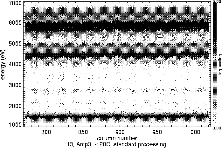
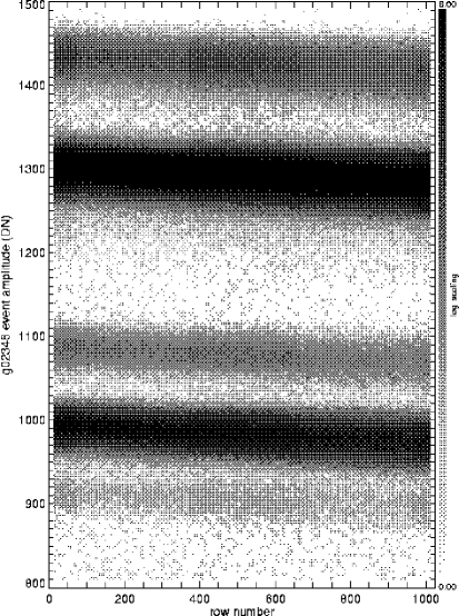
Example spectra for Amplifier 3 (Node D) on the FI device I3 and Amplifier 0 (Node A) on the BI device S3, using a large sample of the appropriate ECS data taken at 120C and all rows of the devices, are shown in Figure 1. These spectra reflect the work of the Chandra X-ray Center (CXC) to remove the largest effect of CTI (illustrated in Figures 2 and 4 below), the row-dependent gain. They represent the standard processing applied to all ACIS data and form the fundamental comparitors for our CTI corrector’s performance.


The data were filtered to keep only events with certain “standard” grades. The ACIS event grading scheme can be related to that of the Japanese X-ray satellite ASCA [16], which is familiar to X-ray astronomers. The standard ACIS grade filtering scheme includes ASCA-like Grades 0, 2, 3, 4, and 6 (“g02346”, [18]) and was developed (in the absence of CTI) to maximize both sensitivity and spectral resolution (see the “Chandra Proposers’ Observatory Guide,” [15]). Virtually all standard data products employ this grade filter.
2.2 FI CTI
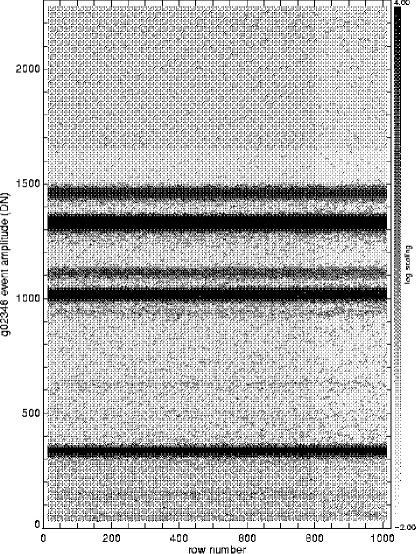
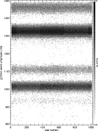
Figure 2 illustrates the effects of CTI on the ACIS I3 chip at focal plane temperatures of 110C (left) and 120C (right) by showing the row-dependent charge loss and energy resolution for the spectral lines in the ECS. The events are binned by position and energy using the Event Browser software [19] into an “image” to make the features easier to see.
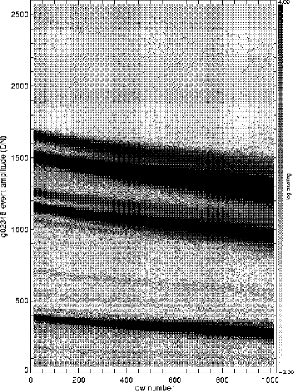
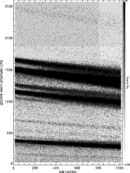
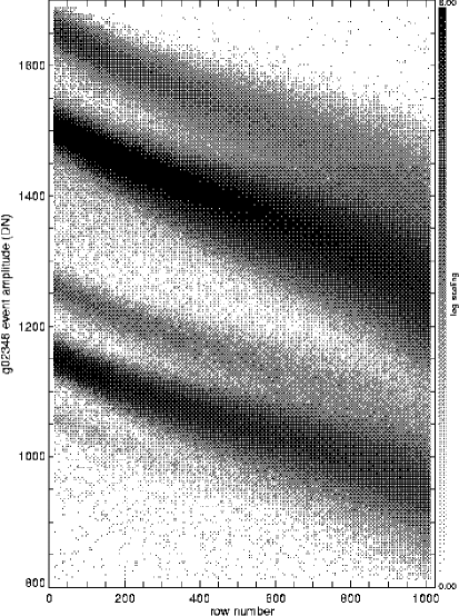
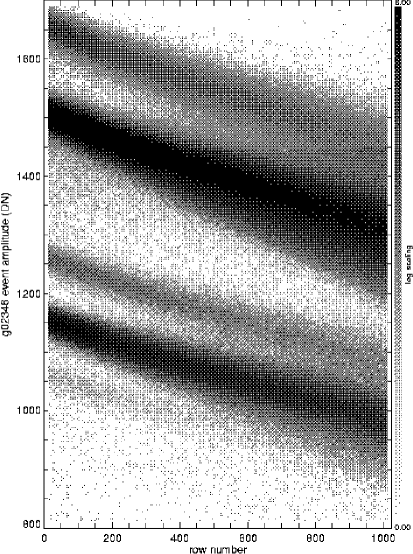
Note that the charge loss gets more severe at higher event energies (the loci in Figure 2 steepen with line energy, or larger DN values). The data are displayed using the digital value (“Data Number,” DN) of the event amplitude because the standard data processing pipeline applies a correction factor to the event energy in eV (a quantity derived from the event amplitude) as a first-order correction for CTI. Since we wish to illustrate this charge loss effect here, we display the data in their native units. For a rough approximation of a line’s event amplitude in DN, divide its energy in eV by 4. We use I3 as the example FI CCD because it contains the aimpoint for the ACIS imaging array. The other I3 amplifiers and other FI devices show similar charge loss effects.
The left-hand panels of Figure 2 are representative of the state of the CTI at 110C and apply to data gathered in the first five months of the mission. The improvement gained by operating at 120C is apparent in the right-hand panels of Figure 2 which show less line blurring at large row numbers.
The lower panels of Figure 2 show expanded views of the Mn and Ti lines. Note the non-linearity of the charge loss with row number that lends a slight S-shape to the curve: the slope is flatter in the middle third of the CCD than at low and high row numbers. Here the increase in linewidth toward the top of the chip (high row number) is easily seen.
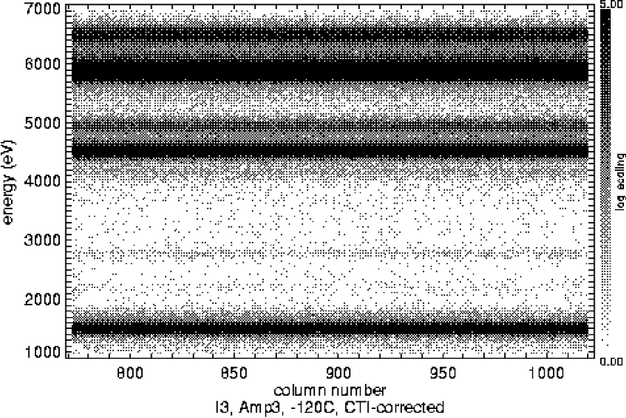
Due to the non-uniform spatial distribution of traps, ACIS CCDs also exhibit column-to-column gain variations that increase in amplitude with energy and row number. These variations contribute substantially to the spectral resolution degradation. Figure 3 illustrates these variations using ECS data from Amplifier 3 of the I3 chip. The data are displayed in energy space now, using the standard processing techniques to remove the gross row-dependent gain variations so that the column-wise variations are more apparent.
2.3 BI CTI
Although CTI in ACIS BI devices is caused by a different mechanism than in the FI devices, it causes similar non-uniformities in the data. The two major differences are that BI devices show CTI in the serial as well as the parallel registers and the framestore is also affected. This means that parallel CTI acts over 2048 parallel transfers in BI devices rather than just 1024 parallel transfers as in the FI devices. The amplitude of serial CTI is much larger than parallel CTI in the BI devices, but there are at most 256 serial transfers. Thus both parallel and serial CTI must be modeled in BI devices and the interaction of these two effects results in spatially-complex charge loss and grade morphing behavior.
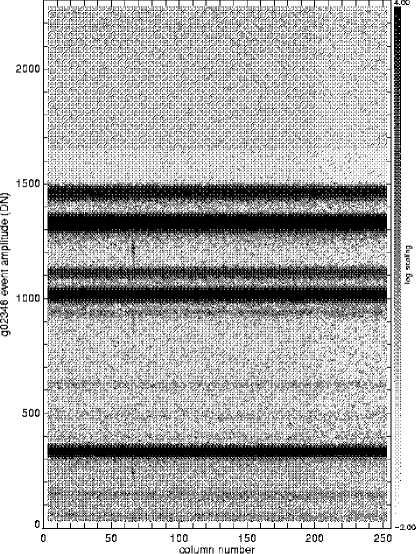
Figure 4 illustrates CTI in the BI device S3, using only data from Amplifier 0 at 120C. BI CTI is only slightly worse at 120C than at 110C, so only 120C data are presented here. The left-hand columns illustrate serial CTI over the full range of the ECS data (top) and for the major spectral lines (bottom). The amplifier readout is at Column 0. The right-hand columns show parallel CTI for the same spectral ranges. Parallel CTI is illustrated using only data from the 64 columns closest to the readout node in order to minimize the effects of serial CTI. As in Figure 2, the data are displayed in their native units (DN) and only standard grades are used.
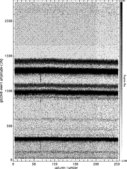
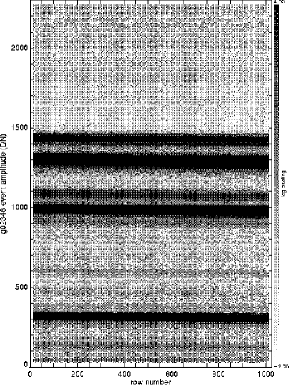
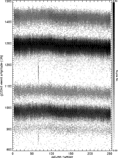
Again due to the non-uniform spatial distribution of charge traps, BI CCDs show column-to-column gain variations that increase in amplitude with energy and degrade the spectral resolution. These variations are visible in the left-hand panels of Figure 4. Also apparent there are charge loss variations of lower spatial frequency.
2.4 Grade Morphing
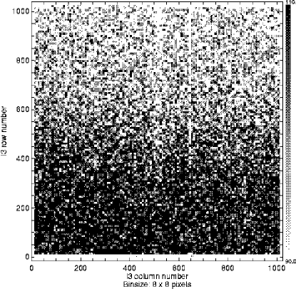
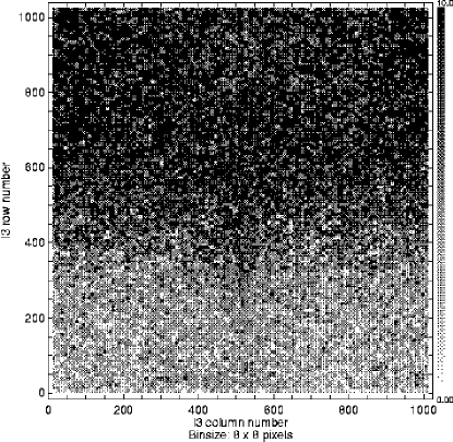
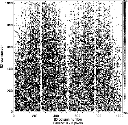
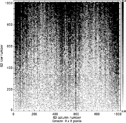
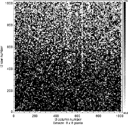
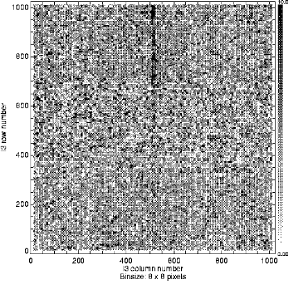
Since CTI causes charge to be shifted into adjacent pixels, thus causing grade morphing, stringent grade filtering results in non-uniform quantum efficiency across the device. Figure 5 shows the number of detected events in the 6 keV Mn K lines in ECS data, using standard grades (g02346, left) and the complementary Grades 1, 5, and 7 (right). The top plots are for the FI device I3 at 110C; at 120C the FI CTI is reduced and the quantum efficiency is quite uniform across the device for the standard grades. The bottom plots are for the BI device S3 at 120C; the behavior at 110C is similar. Note the complex interaction between parallel and serial CTI in the BI device: events morph into Grade 7 due to parallel charge trailing (e.g. top left corner of image), but they morph back out of Grade 7 due to serial charge loss (e.g. top of image around column 300). The degree of grade morphing is a complicated function of event energy and the original event grade. The mirroring effect seen in the BI images is due to the alternating direction of serial readout in the four amplifiers.
3 The Model
3.1 The Primary Model
Our CTI model is phenomenological rather than physical, opting to characterize the effects of CTI in the data rather than to model directly the spatial distribution and time constants of the trap population (see [10], [20], and [21] for examples of such physical models). It consists of a set of amplifier-dependent piecewise-linear equations that relate the quantity of charge lost from a pixel to the original quantity of charge in that pixel. In turn, the amount of charge trailed into the adjacent pixel was determined empirically to be a piecewise-linear function of the charge loss. Trailing is not modeled as an amplifier-dependent relation, rather data from all amplifiers can be combined to derive the fit parameters.
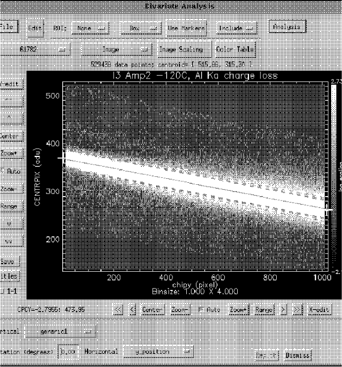
We measure charge loss at a given energy by fitting a line to a plot of the central pixel value (in DN) for only Grade 0 (single-pixel) events as a function of event position on the chip (e.g. row number, called “CHIPY,” for FI devices). All data are fit as an ensemble of points, using sigma-clipping to remove outliers. This is illustrated in Figure 6. We use the Event Browser software [19] for display and fitting. Here the event data are binned into an image for display only; the actual fitting is done on the events themselves, not on binned data.
We show the Event Browser window here because it illustrates details of the fitting process. The ’s show the input to the fitting tool: approximate endpoints of the line and a rough guess at the linewidth (marked at CHIPY 450). The set of dashed lines at the edges of the spectral line show iterations of the sigma-clipping. The final fit is shown as a solid line.
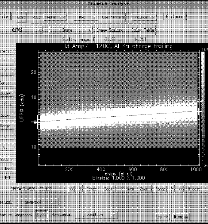
Charge trailing is measured similarly: for FI devices, we plot the “top center” pixel of the neighborhood for ACIS Grade 0 and Grade 64 (upward singly-split) events as a function of CHIPY, then perform a sigma-clipped linear fit to the ensemble of events. This is illustrated in Figure 7, where again we show the Event Browser window to illustrate the input to the fitting routine (’s), the sigma-clipping (dashed lines), and the final fit (solid line).
Our linear characterization of the data leads to a linear model of the charge lost () and trailed () for each pixel, i.e.
| (1) |
| (2) |
where is the number of transfers that the charge packet must undergo to reach the readout node, is the charge in a single pixel, is the charge lost per pixel transfer for an isolated charge packet, and is the charge trailed per pixel transfer for an isolated charge packet. Obviously the physical process of CTI occurs one transfer at a time and the correct model would recalculate the pixel’s charge for each transfer separately (e.g. via a loop in the code), but that is computationally expensive so we do not attempt such a solution.
Accurate modeling of CTI requires accurate knowledge of the shape of and , especially for small charge packets (low energies) where we have very little calibration information. We have found that the grades and energies of corrected events depend on the exact shape of and at low energies. For example, a single linear fit to yields a non-zero intercept, implying that there can be substantial charge loss in pixels originally containing very little charge – this is not supported by the data. This single-line model causes the corrector to boost the charge in low-valued pixels, often causing them to exceed the split threshold (13 DN for both BI and FI devices). This disrupts the grade distribution of a set of monoenergetic events and causes the split events in that set to exhibit higher energies than single-pixel events. We have determined empirically that and must pass through the origin to yield realistic grades and energies for monochromatic input photons.
Thus we model and as piecewise linear, continuous curves that are required to pass through the origin (see Figure 8). Three lines are needed for and two for . The functions’ values (for both parallel and serial CTI) are stored as lookup tables that are accessed for each pixel of each event. We chose a set of lines as the functional form for these relations because they adequately fit the data, they keep the model simple, and because we can restrict the coefficients to ensure zero charge loss or trailing when there is zero charge present.


Our original model for 110C FI data [11] employed a power-law fit, which worked well for all measurable energies up to 6 keV, but underfit the Au L line at 9.7 keV. Application to the first Galactic Center observation made by ACIS showed that this underfitting might be affecting observations of astrophysical iron lines (Y. Maeda, private communication), so the power-law model was abandoned in favor of the piecewise linear model. The new model improves the 110C corrector performance at high energies without compromising the low-energy accuracy. For the more modest FI CTI effects seen at 120C and for BI devices, the power law fit is adequate [22] but we choose to use the piecewise linear model for all temperatures and devices for consistency.
For the BI devices, we must model parallel and serial charge loss and trailing independently to match the data. There are charge traps in the imaging array, framestore array, and serial register. Since the FI devices were damaged by radiation that penetrates only a few microns into the device [7], their (shielded) framestore arrays and serial registers are protected. So, although the CTI is more pronounced on FI devices, it is easier to model than in the BI devices.
The primary FI CTI model consists of a piecewise linear fit to the measurements of parallel charge loss per pixel transfer as a function of line center (in DN units), measured using only the central pixel of Grade 0 events and on a per-amplifier basis. The components cover the ranges 0–100 DN (0–0.4 keV), 100–550 DN (0.4–2.2 keV) and 550–2500 DN (2.2–10 keV) (see the left panel of Figure 8). The mid-energy line is necessary to accomodate a known turnover around these energies (known from calibrations with the soft supernova remnant E0102-72.3). The break is wherever the mid- and high-energy lines meet and is calculated in the code. The low-energy line takes over at 100 DN, a value determined roughly by looking at the energies of corrected split events in the S3 (BI) device. It forces the model through the origin. As mentioned above, this was necessary to avoid anomalous energies for low-energy split events in S3 – in effect, it forces the model to assume zero charge loss for zero-energy events.
An example of the charge trailing model is shown in the right panel of Figure 8. For trailing, only two lines were necessary to fit the data; the low-energy line is forced through the origin as in the loss model. The break between the lines is taken as the loss value where the third line takes over in the loss model (averaged over the four amplifiers). For the example in Figure 8, the two lines in the fit have very similar slopes. Note that the Au L points are omitted from the trailing model. Due to the large charge cloud size and confusion with background events, our method for measuring charge trailing proved unreliable for Au L .
The (very small) error bars represent only measurement uncertainty (estimated by fitting each line 3 times); we have not attempted to quantify systematics. The high-energy charge loss fit was made using errors in both line centers and charge loss and used all points shown on the plot above 500 DN. The low-energy charge loss fit only includes the Al K and Mn/Fe L-complex points.
A similar approach is taken for the BI devices. First the serial charge loss and trailing model coefficients are determined for each amplifier, also using a 3-component piecewise linear fit for loss and a 2-component piecewise linear fit for trailing. Then the CTI corrector (described below) is run on the data, with coefficients for parallel CTI set to zero. The resulting serial-corrected data are used to measure the coefficients for parallel CTI. Due to non-linearities in the serial CTI, columns near the edges of each amplifier are excluded when computing the linear parts of both the serial and parallel models.
As a check on the functional form of the model at low energies, we measured the low-energy parallel charge loss using the soft supernova remnant E0102-72.3 (“E0102”), a calibration target for Chandra. Figure 9 shows the charge loss model for I3, Amplifier 2, at a focal plane temperature of 110C, with the E0102 charge loss values overplotted for the three soft lines measurable with these data.

The E0102 points were obtained from two datasets, Observation ID 49 (source placed at CCD row number ) and Observation ID 48 (source placed at CCD row number ). The charge loss per pixel transfer was calculated using only these data, then corrected for the fact that the full-chip charge loss slope is more shallow than that calculated when only using the bottom half of the chip by executing a similar half-chip analysis on ECS data, then determining the correction factor necessary to recover the full-chip slope.
The E0102 data were not used to modify the model. Their agreement with the low-energy model components confirms that the 3-line fit chosen to parameterize the charge loss is reasonable down to keV at least. This is adequate for characterizing FI devices but we have no confirmation of our model in the 0.2–0.5 keV range accessible to BI devices.
3.2 Shielding Within an Event
This CTI model is “local” – prediction of the amount of charge lost by a particular event does not consider the possibility that another event falling in the same columns but closer to the amplifier readout will have filled some portion of the traps, reducing the charge loss from its nominal value (see [20] and [14] for descriptions of such “precursor” models). We do however consider shielding effects that may occur within the nine pixels of a single event. Physical principles suggest that pixels which are not isolated experience loss and trailing that are influenced by their neighbor pixels – what we call the “self-shielding” effect. We hypothesize that the loss mechanism essentially acts only on the portion of a pixel’s charge which exceeds the charge in the previous pixel; similarly the trailing mechanism essentially acts only on the portion of a pixel’s charge which exceeds the charge in the following pixel. Thus a given pixel experiences either loss or trailing, not both – loss if its predecessor has less charge than the pixel in question and trailing if its predecessor has more charge.
The physical process of self-shielding is of course governed by the relationship between the physical volume of silicon occupied by one pixel’s charge packet compared with the physical volume of silicon occupied by its predecessor or successor charge packet. A physically-based model of self-shielding would involve knowing the details of the three-dimensional charge distribution [20]. For our phenomenological model, we instead take a very simple approach to modeling this effect.
For a pixel with charge (“root”) whose predecessor (“lead”) has a smaller charge , we compute:
| (3) |
| (4) |
| (5) |
The effective charge loss is then subtracted from .
For a pixel with charge (“root”) whose predecessor (“lead”) has a larger charge , we compute:
| (6) |
| (7) |
| (8) |
The effective charge trailed is then added to . In this model, events which are almost evenly split between two pixels in the direction of transfer suffer CTI effects almost identical to those experienced by a Grade 0 event with half the energy of the split event.
3.3 Deviations from Linearity
Although ACIS FI devices do not exhibit serial CTI, they do show a small charge loss effect which is proportional to the distance between the interaction site and the left or right edge of the CCD (as opposed to the distance to the amplifier readout). This is believed to be caused by the slight drop in clocking voltages necessarily suffered between the middle of the CCD and the supply leads at the chip edges (M. Bautz, private communication). CTI scales the effect so that these gain variations are row- and energy-dependent, with the bottom rows of the chip showing virtually no variation and the top rows varying by up to 100 DN at high energies (6 keV).
ACIS BI devices also show low-spatial-frequency deviations from linearity in their charge loss. As shown above, by combining large numbers of ECS observations, column-to-column gain variations can be seen. (Row-to-row variations are not seen in either FI or BI devices.) These effects are also energy-dependent, with high-energy calibration lines in the ECS exhibiting larger-amplitude variations than low-energy lines.
These nonlinearities result in broadened spectral lines for both FI and BI devices even after correction for linear charge loss and trailing. Thus we have developed the concept of a “deviation map” to make moderate gain adjustments to each event that help to regularize the CCD response across the device and narrow the linewidths. Our techniques are reminiscent of flat-fielding techniques used to remove instrumental non-uniformities in visual CCD data.
We model the deviations via a 2-dimensional map () with an energy-dependent amplitude:
| (9) |
where and are the position coordinates of the event in units of CCD pixels, = event amplitude in DN, = deviation amplitude, and is the two-dimensional map of deviations extrapolated to 0 DN. The value of this deviation is calculated for each event based on its location and applied as an additive adjustment to the central pixel value. Figure 10 shows images of for I3 and S3 at 120C. Cuts through the I3 map, given in Figure 11, show that the amplitude of the deviations increases substantially with on FI devices, as noted above.
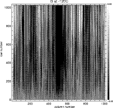
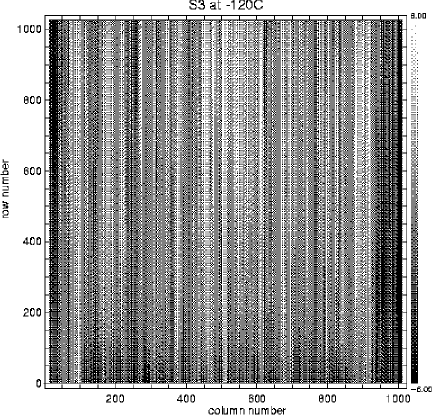

The zero-energy deviation map is made for each amplifier in a series of smoothing and averaging steps using constituent maps made in the three strongest lines in the ECS: Al K , Ti K , and Mn K . First the ECS data are CTI-corrected using the linear model described above. The resulting event list is filtered spectrally to keep only events in one of these strong lines. We then make an image of these event amplitudes in DN space, binned by 1 pixel in and by 16 pixels in , with intensity computed as a sigma-clipped mean. This process is repeated for the other two lines, resulting in three images of the deviations covering a substantial range in energy.
For each energy, we then perform a trending analysis of gaussian fits to the spectral line, noting the mean and standard deviation (width) of the spectral line as a function of row number. We perform a linear fit to these trended properties to determine the line energy and width at row zero, where the values are unaffected by CTI. Then we plot the row-zero standard deviations as a function of line energy (in DN) and fit a line, noting its slope (S) and intercept (). This gives the equation
| (10) |
which, by analogy to the definition of the deviation map above, yields
| (11) |
We obtain an estimate of and for each amplifier; these are averaged then divided to obtain .
The maps at Al K , Ti K , and Mn K are then smoothed column-wise to reduce the effects of shot noise. Next we generate three estimates of using the smoothed maps and average those three estimates to obtain our final for that amp. Lastly, the maps for each amplifier are incorporated into an array to make one deviation map for the entire CCD.
This deviation map is used to adjust the amplitude of an event. We compute in Equation (9) above by summing the values of pixels in the event neighborhood that are above the split threshold (13 DN). The adjustment is then computed from Equation (9), using the event’s location to access the correct element of . The adjustment is made by adding the result to the central pixel of the event. This preserves the event grade; we determined by experimentation that this technique produces the best reconstructed event.
4 Simulator Results
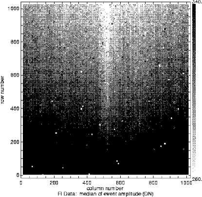
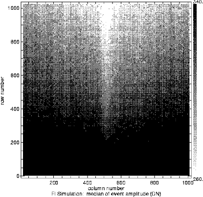
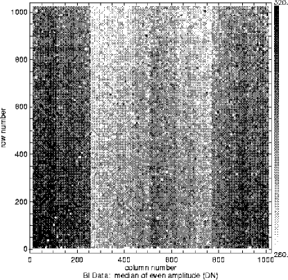
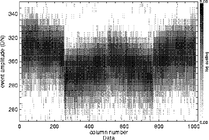
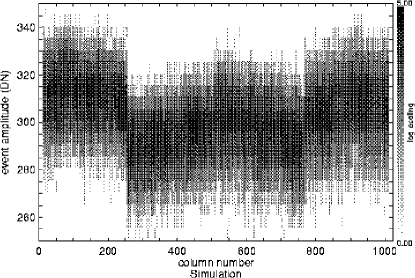
The Monte Carlo simulator’s ability to reproduce the effects of CTI is illustrated in the following figures. All data and simulations are for Al K (1.486 keV) with ASCA g02346 grade filtering. In both figures, the left panels show the data and the right give the matching simulations.
The upper panels of Figure 12 show images of the median event amplitude events on an FI device (I3 at 120C). Both datasets contain events and are binned at pixels. With this binning, column-to-column variations are not visible, but variations with lower spatial frequency are clear and are reproduced with good fidelity by the simulator.
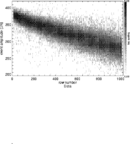
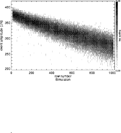
When modeling CTI for the event simulator, we add noise to the pixel adjustments to model the stochastic nature of traps. We find that a simple Poisson noise model on the number of electrons lost is not sufficient for FI devices, so we introduce an energy-dependent tuning parameter that is multiplied by the event’s row number to account for the additional line broadening with increasing distance from the readout node that is seen in the ECS data. The effects of this are apparent in the lower panels of Figure 12. Row-dependent non-linearities in the CTI give the data a slight S shape in this plot; this feature is also seen in the simulation.
The data here show more scatter than the simulation; this is due in part to the background in ECS data and to Al K events that occurred in the framestore region of the CCD. These framestore events do not suffer CTI and appear as a faint horizontal band in the lower left panel of Figure 12.
The upper panels of Figure 13 show the same Al K map as Figure 12, now for the BI device S3. As the figure clearly shows, the four amplifiers in the S3 device have slightly different responses. This is reproduced well by the simulation, as are the CTI-induced spatial variations. The column-wise variations in the Al K event amplitudes are shown in the lower panels of Figure 13. Again the simulator does a reasonable job of reproducing these variations. Both the imaging and the framestore sections of BI CCDs suffer CTI, so no horizontal band of CTI-free events is seen in the lower left panel of Figure 13.

5 The Corrector
As mentioned above, we have used our Monte Carlo modeling of CTI effects to build a CTI corrector. This program attempts to remove those effects from individual ACIS events, taking a forward-modeling approach. For each observed event we first hypothesize the nine pixel values of a corresponding clean event , i.e. the event that would have been obtained if no CTI effects were present. This clean event is passed through the CTI model, producing a model event which estimates what we should have observed if our clean event hypothesis is correct. The hypothesis (the nine pixel values of ) is then adjusted using the differences between the observed event and the model event in a simple way:
| (12) |
This iterative process continues until the model and observed events differ by less than 0.1 DN (for each of the 9 pixels). When convergence is obtained, C is returned as the CTI-corrected event.
Tests show that when a limit of 15 iterations is imposed within the corrector a trivial number of events fail to meet the 0.1 DN convergence criterion; this limit is imposed as a safety in the code and the number of iterations needed for convergence (typically 3–5) is recorded for every simulated event. The pixel values and thus the event amplitudes produced by the corrector are real numbers.
Because the corrector operates on event islands (33 pixel arrays) rather than on event amplitudes, it has the potential to improve the grades in an event list, leading to a different grade distribution. Thus the CCD quantum efficiency appropriate for grade-filtered corrected data will differ from that appropriate for similarly grade-filtered uncorrected data. A technique for determining this QE adjustment is presented in Section 7.
The CTI corrector consists of a set of IDL [23] programs and device-dependent parameter files that instantiate the model for each amplifier on each CCD, for a given epoch of the Chandra mission. Obviously observations must be configured to telemeter the pixel event island in order for the corrector to modify that island. The corrector operates on the “Level 1” event list, one of the standard data products, and requires no additional information regarding the observation. The parameter tuning presumes that the CCDs were operated in their standard full-frame mode, with a frame readout time of 3.24 seconds. Since the trap time constants interact with this readout time to affect the average number of filled traps, observations made in any of the “sub-array” modes (including Continuous Clocking Mode) will exhibit different CTI and cannot be corrected using this full-frame tuning.
The code is available and may be of interest to other groups concerned with the results of radiation damage on X-ray and visual CCD detector systems and to Chandra/ACIS users. We have recently completed tuning our CTI corrector for all chips in the ACIS-I array and chips S2 and S3 in the ACIS-S array, for focal plane temperatures of 110C and 120C. We provide the parameter files used by the corrector code on our webpage, so any Chandra/ACIS user with data on one or more of the allowed CCDs may experiment with the PSU CTI corrector.
Response matrices have been generated for these device/temperature combinations as well, using the CTI model as part of the Monte Carlo CCD simulator to generate simulated events at a large number of monochromatic energies. The simulator applies CTI to the events, then the corrector is used to remove the non-random effects of CTI. The resulting events are combined into a (now polychromatic) instrumental spectrum, which represents a single row of the response matrix. An example was shown in T01. These response matrices are also available to Chandra/ACIS users.
6 Corrector Results
6.1 Spectral Resolution
The most fundamental result of CTI correction is the improvement in spectral resolution. This is illustrated in Figure 14 for an FI device at two ECS energies. This figure also illustrates the major improvement in FI spectral resolution made by reducing the ACIS focal plane temperature from 110C to 120C. The CTI corrector improves the resolution at both focal plane temperatures and all energies for the uniform illumination of the ECS. Celestial sources, which tend to be more pointlike and thus suffer less from the variations across the CCD than ECS data, will show less dramatic improvement.


Figure 15 shows the ECS spectral resolution improvement with CTI correction on a BI device, now as a function of energy rather than position, as the BI devices do not exhibit position-dependent resolution. Only 110C data are shown here; 120C results are similar. Again the spectral resolution is improved at all ECS energies. Below 1.5 keV, though, the device’s intrinsic resolving ability dominates the CTI effects. Here, CTI correction will not markedly improve the spectral resolution. As for FI devices, the spectral resolution improvement for more pointlike celestial sources will be less dramatic.

Comparing Figures 14 and 15 shows that the best ACIS spectral resolution is achieved by placing targets on the lower half of ACIS FI devices. In these regions, the FI resolution surpasses the BI resolution. Without CTI correction, only the lowest quarter of the FI devices surpassed the BI resolution. This improvement is particularly important for targets with extended emission or point sources distributed across the field, such as star formation regions [24] and the Chandra Deep Field observations of the X-ray background [25].
6.2 Spectral and Spatial Comparisons
To give more detail on the effects that the CTI corrector has on ECS data, figures identical to those in Section 2 are presented below.
Figure 16 shows CTI-corrected ECS spectra. For ease of comparison, in this one case we reproduce Figure 1 in the top two panels and show the CTI-corrected spectra below. The spectral resolution is improved for both FI (left) and BI (right) spectra.


The performance of the corrector in removing the observed spatial variation of event amplitude in FI ECS data is shown in Figure 17. The corrector has largely removed the gain changes across the device; compare to Figure 2. Since the spectral broadening with row number is primarily the result of a random process involving one of the trap species [26], it cannot be completely suppressed in our reconstructed events.
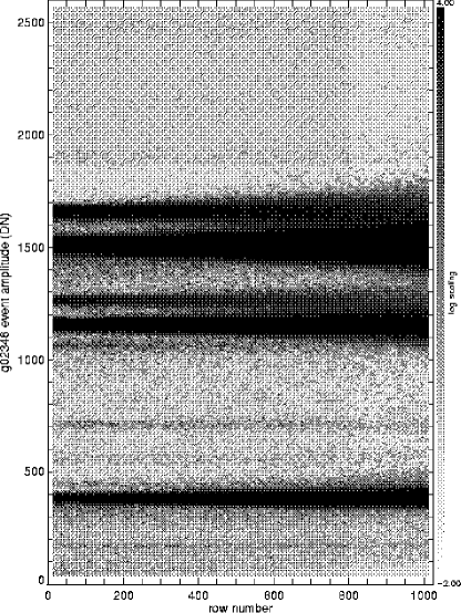
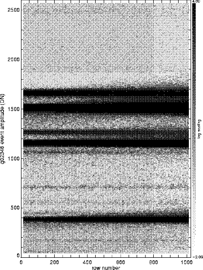


Figure 18 illustrates the remaining non-uniformities after the CTI corrector, with its deviation map, is used to remove the column-dependent gain variations caused by CTI. Comparing this to Figure 3, it is clear that accounting for column-to-column gain variations improves the quality of the data.
Now turning to a BI device, Figure 19 shows the ECS data from S3, Amplifier 0, at 120C, after CTI correction. The spatial effects of CTI are much more subtle on BI devices than on FI devices; the most obvious improvement compared to Figure 4 is in the lower left panel, where the column-to-column gain variations have been largely suppressed by the CTI corrector.

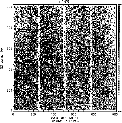
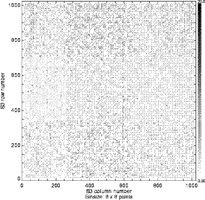
Finally, Figure 20 shows the grade-specific 6 keV images from Figure 5 after CTI correction. The position dependence of undesirable grades (1, 5, and 7) is much reduced.
6.3 Event Grades
As mentioned above, grade morphing due to CTI is a substantial concern for FI observations early in the mission, due to the higher focal plane temperature of 110C. This problem was largely solved by lowering the focal plane temperature, but it is worth noting here the effects at 110C for archival researchers.
Figure 21 shows the effect of grade-morphing on the 110C FI detector quantum efficiency, for the Mn K and Mn K lines combined. At this energy, many events are lost forever because they morphed into grades that were not telemetered. For low-energy events (e.g. Al K) even at 110C, the charge is more spatially concentrated, leading to more single-pixel events. CTI causes these to morph into grades that are still captured in the standard grade filtering, so the QE at the top of the device is not affected by CTI.
For this high-energy dataset, keeping all grades, there are 12% fewer events at the top of the chip compared to the bottom due to grade morphing and subsequent on-orbit grade rejection. For standard grade filtering with standard processing, this loss is augmented to 20% at the top of the chip. This is because grade morphing caused events to migrate out of acceptable grades. By applying the standard grade filter after applying the CTI corrector, though, there are only 13% fewer events at the top of the chip compared to the bottom. Since this is similar to the curve for all grades, we can conclude that we have recovered virtually all useful events available on the ground.

For the BI devices, grade morphing is an issue even at 120C. The success of the CTI corrector in regularizing the grade distribution for the top half of a BI device (where grade morphing is most pronounced), using on-orbit ECS data on the S3 chip at 120C, is shown in Table 2, where original and corrected ASCA-like grade distributions are listed for the Al, Ti, and Mn calibration lines.
Some events are not recovered into their original grades because the corrector is unable to recover charge that has been eroded by CTI down below the split threshold. At that level, the charge is indistinguishable from noise and the corrector is purposely not allowed to include such pixels in its reconstruction.
A good test of grade recovery is to compare the number of Grade 2 events to the sum of Grade 3 and Grade 4 events – for devices with no CTI, these quantities should be roughly the same. Applying this diagnostic to Table 2 shows that the corrector is quite useful in recovering appropriate grades.
| ASCA | 1.486 keV | 4.511 keV | 5.895 keV | |||
|---|---|---|---|---|---|---|
| grade | Standard (%) | Corrected (%) | Standard (%) | Corrected (%) | Standard (%) | Corrected (%) |
| 0 | 26.7 0.1 | 30.9 0.1 | 13.5 0.0 | 22.0 0.1 | 14.9 0.0 | 28.7 0.0 |
| 1 | 0.0 0.0 | 0.0 0.0 | 0.0 0.0 | 0.0 0.0 | 0.0 0.0 | 0.0 0.0 |
| 2 | 30.8 0.1 | 25.3 0.1 | 30.8 0.1 | 20.3 0.1 | 33.2 0.0 | 18.4 0.0 |
| 3 | 10.1 0.0 | 12.1 0.0 | 6.1 0.0 | 11.2 0.0 | 5.0 0.0 | 10.2 0.0 |
| 4 | 9.9 0.0 | 12.3 0.0 | 6.0 0.0 | 11.4 0.0 | 4.9 0.0 | 10.4 0.0 |
| 5 | 0.3 0.0 | 0.4 0.0 | 0.7 0.0 | 0.5 0.0 | 0.8 0.0 | 0.4 0.0 |
| 6 | 21.8 0.1 | 18.9 0.0 | 39.6 0.1 | 34.4 0.1 | 37.1 0.0 | 31.6 0.0 |
| 7 | 0.3 0.0 | 0.0 0.0 | 3.3 0.0 | 0.2 0.0 | 4.2 0.0 | 0.2 0.0 |
Grade-dependent BI spectra are shown in Figure 22: the left-hand panel gives the results for standard processing and the right-hand panel those for the CTI corrector. Between 1 and 7 keV, it appears that including ASCA grades 1, 5, and 7 might improve the signal-to-noise ratio in CTI-corrected data, as the ECS spectral lines dominate over the background spectrum. In general, though, CTI correction has restored the original intent of ASCA g02346 grade filtering, to suppress the particle background and improve signal-to-noise across the full spatial and spectral range of the device.


6.4 Gain linearity
Once the CTI corrector is applied to adjust the amplitude and grade of each ACIS event, the DN-to-eV conversion is recomputed using the ECS lines. A linear fit is made to obtain the gain (slope) and offset (y-intercept) for each amplifier. We can then compute the difference between the measured ECS line energies and the values predicted by this linear model; these residuals are a measure of the non-linearity of the amplifier after correcting for CTI in the data. Figure 23 shows the ECS line energy residuals for all amps on I3 (left) and S3 (right) at 120C.


These residuals show that a linear gain model is reasonable for CTI-corrected ECS data on FI devices at all relevant energies; deviations are seldom larger than eV. For the BI device S3, the deviations are larger at energies below 2 keV. The ECS line complex at 680 eV is faint and more information is needed to search for gain non-linearities in the important BI spectral range 0.2-0.5 keV. Unfortunately virtually no calibration information at such low energies is available at this time.
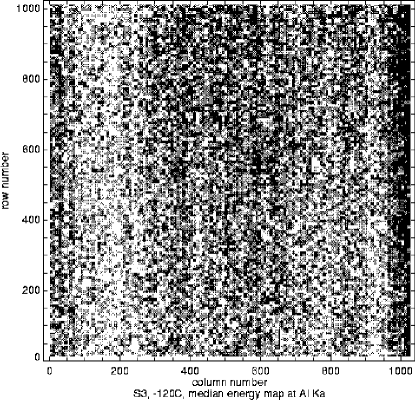
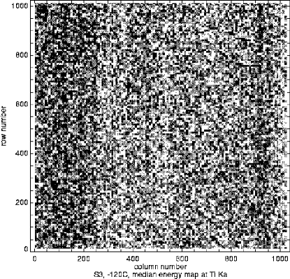
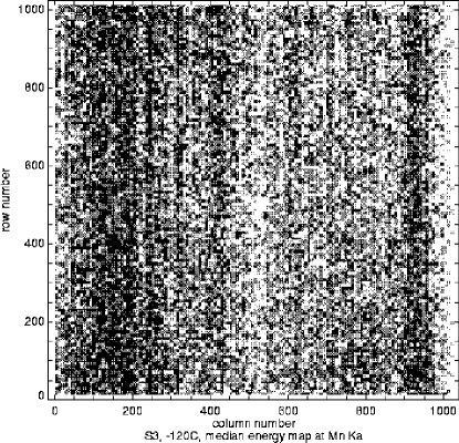
Figures 24 and 25 show the position dependence of gain variations remaining after CTI correction. Three median energy maps are given, for the three main ECS lines. These greyscale maps are displayed such that black is from the mean energy and white is from the mean energy. The spectral lines are shown in the right panels.
For the FI device I3 at 120C, Figure 24 shows that there is some remaining structure following amplifier boundaries. There is no clear correlation between energies, however; regions that are light at one energy are neutral or dark at another. Thus the algorithm, although imperfect, appears to be removing gain variations in a reasonable way.
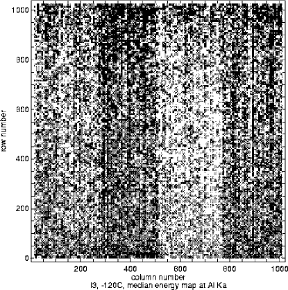

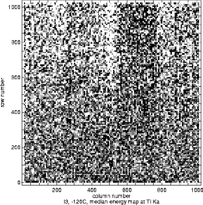


Figure 25 shows that the same is true for the BI device S3. Non-random gain deviations exist, but they are not correlated across energies. It might be possible to generate a second-stage deviation map to try to remove these residual features, but our attempts using this dataset (roughly one year of ECS observations) have been unsuccessful.



7 Quantum Efficiency Adjustments
As mentioned above, grade adjustments by the CTI corrector combined with subsequent grade filtering result in CCD quantum efficiency improvement. This change in QE must be incorporated into the ACIS calibration products so that source fluxes can be estimated properly. Since the CTI-induced grade morphing changes with position on the CCD, the most direct way to account for these QE changes is via the Quantum Efficiency Uniformity (QEU) files, one component of the Auxiliary Response File (ARF) used in spectral fitting. The ARF incorporates the vignetting function of the telescope, the positionally-averaged QE of the CCD, and position-dependent deviations from that average QE via the QEU files.
Two approaches to adjusting the QEU files for CTI-corrected data are necessary: one for FI devices that were effectively CTI-free before launch, and a second for BI devices that have always suffered measurable CTI. These are described below.
7.1 Estimating QE Loss with Respect to an Undamaged Device
This approach is used for FI devices. We estimate how the QE of undamaged devices changes when the damage is applied and the resulting events are corrected for CTI (for example by the simulation experiments shown in Figure 26). Such a loss is of course a function of both energy and position on the CCD. Then the QEU files that were constructed for undamaged devices are adjusted downward to account for unrecoverable CTI losses. For each energy ,
In this formulation, the & terms are the mean QE and QE uniformity products produced by standard processing for undamaged devices, and the term expresses the QE lost by the damage plus correction process. For ACIS FI devices the term is not actually a function of X (CCD column number). The pre-launch FI QE is very spatially uniform below 8 keV, consistent with unity to within measurement errors [16]. Thus for ACIS FI devices the term above is set to unity.

7.2 Estimating QE Recovery with Respect to a Damaged Device
This approach is used for BI devices. We estimate the QE recovery of the CTI corrector via simulation/correction experiments, as shown in Figure 27. This recovery is also a function of both energy and position on the CCD. Then QEU products that were constructed for damaged devices are adjusted upward to account for the increased QE after CTI correction. So for each energy ,
In this formulation, the and terms are the mean QE and QE uniformity products generated by standard processing for damaged devices, and the term expresses the QE recovered by the correction process.

8 Model Performance on Celestial Data
There is an uncertainty introduced by using on-orbit calibration data to tune this or any other model: we must assume that the CTI measured by the on-orbit calibration source is representative of that present in celestial data. This assumption could be incorrect, even for celestial data obtained at nearly the same time as the calibration data, due to differences in the count rates (photons plus particle background) between these two configurations. It is important to remember, however, that most ACIS events are due to particle interactions and are not even telemetered, so the event list supplied to the user is not representative of all the potentially trap-filling interactions that occurred. Since most of these particle events are from cosmic rays that enter from all angles and are not absorbed by the Observatory structure, it is reasonable to assume that calibration and celestial data have comparable particle fluxes, thus a comparable trap population.
We have used the instrumental Au L (9.7 keV) and Ni K (7.5 keV) lines as rough diagnostics of the corrector’s performance on celestial data. These spectral features are due to fluorescence from hardware components. The lines are faint, but in long exposures it is possible to measure their gain changes with position on the chip just like we measure lines in the calibration data. The tests show that the corrector works fairly well even at these high energies, reducing the charge loss per pixel transfer by a factor of 10.
Another implication of tuning the corrector to the ECS data is that we have only minimal calibration information below the Al K line at 1.486 keV and no information below the Fe-Mn L complex at 680 eV. We have extrapolated to lower energies using fits of sensible functional forms, but it is likely that our assumptions break down for small amounts of charge. Understanding the behavior of the CCDs between 0.2 and 1.5 keV is important for obtaining accurate hydrogen column densities, comparing ACIS results to findings from other X-ray missions, and inferring valid astrophysics for the large number of soft sources Chandra is examining.
We can use celestial data to test and improve our calibration of the CTI at low energies. The best available target is the supernova remnant E0102-72.3 (“E0102”) in the Large Magellanic Cloud, used as a soft calibration source for Chandra. We used this source in Figure 9 above to confirm that the piecewise-linear CTI model was reasonable at low energies.
Figure 28 shows the difference between measured and true line energies from ECS data and the E0102 soft spectral lines. Energies for the E0102 lines were provided by R. Edgar (private communication) and can be inferred from Rasmussen et al. [27]. This shows that the model can recover reasonable line energies for both FI and BI devices down to 0.5 keV. The I3 plot includes E0102 points obtained from combining Observation ID’s 136, 140, 439, 440, 1314, 1315, 1316, and 1317. The S3 plot includes E0102 points obtained from combining Observation ID’s 141, 1308, 1311, 1530, 1531, and 1702.


Since E0102 has been observed at several off-axis positions on I3, we can compare its standard and CTI-corrected spectra as a function of the position-dependent spectral resolution. Figure 29 shows these spectra, with the spectral resolution increasing with off-axis angle (the I-array aimpoint is at the top of the I3 chip, where CTI-induced spectral resolution degradation is at its worst). All spectra used ASCA g02346 grade filtering, a binsize of 10 eV, and were smoothed with a Gaussian of width 1 bin.


Near the aimpoint, the CTI corrector changes the low-energy gain substantially and improves the spectral resolution. At 4 arcmin off-axis (about half-way up the I3 chip) the spectral lines are noticeably narrower. The CTI corrector applies a more modest gain change and still improves the spectral resolution compared to standard processing. At 7 arcmin off-axis (only 100 rows from the bottom of the chip, where CTI is minimal), standard and CTI-corrected spectra are very similar in gain and spectral resolution. The line energies between the three observations are comparable in CTI-corrected data.
9 Summary
We have developed a phenomenological Monte Carlo model of CTI in both front- and back-illuminated ACIS CCDs and used it to devise a CTI corrector for ACIS observations of celestial X-ray sources. The PSU CTI corrector has been tuned for the ACIS CCDs most often used for imaging: I0–I3, S2, and S3. This tuning uses a composite dataset of observations of the ACIS External Calibration Source. Both major focal plane temperatures (110C, September 1999 – 29 January 2000, and 120C, 29 January 2000 – present) are calibrated.
The CCD simulator and CTI corrector IDL source code are provided to the community111http://www.astro.psu.edu/users/townsley/cti/. Also available are the parameter files that instantiate the simulator and corrector tuning for each device, the modified QEU files, and a suite of response matrices for use with CTI-corrected data.
The corrector works on a Level 1 event list from ACIS observations using the full-frame readout mode. The or pixel event islands must be included in order for the corrector to modify the event grade. The user is then required to perform the other filtering steps (grade filtering, applying Good Time Intervals, etc.) to recover the CTI-corrected Level 2 event list.
Refinements of the model since the original report of this work (in early 2000) [11] have led to several improvements in CTI-corrected data:
-
•
Modeling the charge loss per pixel transfer as three lines improves the fidelity of corrected event amplitudes at high energies without compromising the low-energy results.
-
•
Removing column-to-column gain variations (to the degree possible with this model) improves the energy resolution on both FI and BI CCDs.
-
•
Including charge trailing and shielding within a single event makes it possible to compensate for CTI-induced grade morphing at all event locations.
-
•
Using a more extensive set of calibration observations of the soft SNR E0102-72.3, we have improved the model tuning in the spectral range 0.5–1.5 keV.
Since this corrector does not account for precursor events, we cannot totally eliminate the row-dependent energy resolution of the FI devices. Thus position-dependent response matrices are still necessary for accurate FI spectral fitting. By regularizing the gain and grade distributions across these CCDs, though, we have reduced the number of matrices needed for typical analysis tasks to fewer than 10. For BI devices, the improvement is even better; since S3 does not exhibit position-dependent energy resolution, a single S3 response matrix is usually adequate for CTI-corrected data. This is a great simplification for users, especially those working on extended targets such as supernova remnants or clusters of galaxies.
Lowering the ACIS focal plane temperature to 120C achieved dramatic reduction in the effects of CTI on FI devices. This reduced the FI spectral resolution degradation and its row-dependence, moderated the gain changes across the device, and reduced the charge trailing, resulting in much less high-energy quantum efficiency loss at the top of FI devices. Since a large fraction of ACIS data were obtained at 120C, we have concentrated on those data in this paper. It is important to remember, however, that the early days of the mission included observations of some very exciting targets and those data are now publicly available. So for the sake of archival research, we have invested substantial effort in tuning the CTI corrector at 110C.
The CTI corrector has been used for a variety of Chandra investigations, including:
- •
- •
-
•
Supernova remnants, e.g. [31]
-
•
The starburst galaxy M82 [32]
-
•
A search for low-luminosity active galactic nuclei [33].
All parameter files, source code, and instructions comprising the PSU CTI corrector and the PSU CCD simulator are available on the Web222http://www.astro.psu.edu/users/townsley/cti/. We encourage the use of these tools and welcome feedback.
Other software mitigation techniques for CTI are under development at the Chandra X-ray Center and at MIT, with support by Chandra Project Science at Marshall Space Flight Center and the rest of the Chandra team. The MIT/ACIS group also is working to devise hardware mitigation techniques that may further reduce the effects of the radiation damage. Prigozhin et al. [8], [9] are developing a more physical model of the charge traps that is likely to replace this phenomenological model. We are confident that these efforts will eventually lead to a more robust CTI correction scheme for ACIS data.
References
- [1] M. Bautz, M. Pivovaroff, F. Baganoff, T. Isobe, S. Jones, S. Kissel, B. LaMarr, H. Manning, G. Prigozhin, G. Ricker, J. Nousek, C. Grant, K. Nishikida, F. Scholze, R. Thornagel, G. Ulm, X-ray CCD calibration for the AXAF CCD imaging spectometer, in: X-Ray Optics, Instruments, and Missions, Vol. 3444, SPIE, 1998, p. 210.
- [2] B. Burke, J. Gregory, M. Bautz, G. Prigozhin, S. Kissel, B. Kosicki, A. Loomis, D. Young, Soft X-ray CCD imagers for AXAF, IEEE Trans. Electron. Devices 44 (10).
- [3] G. Pavlov, J. Nousek, Charge diffusion in CCD X-ray detectors, Nucl. Instr. and Meth. in Phys. Res. A 428 (1999) 348.
- [4] L. K. Townsley, P. S. Broos, G. Chartas, E. Moskalenko, J. A. Nousek, G. G. Pavlov, Simulating CCDs for the Chandra Advanced CCD Imaging Spectrometer, Nucl. Instr. and Meth. in Phys. Res. A in press.
- [5] G. Prigozhin, A. Rasmussen, M. Bautz, G. Ricker, A model of the X-ray response of the ACIS CCD, in: X-Ray Optics, Instruments, and Missions, Vol. 3444, SPIE, 1998, p. 267.
- [6] G. Prigozhin, J. Woo, J. Gregory, A. Loomis, M. Bautz, G. Ricker, S. Kraft, X-ray absorption near edge structure in quantum efficiency of X-ray CCDs, Optical Engineering 37 (10) (1998) 2848.
- [7] G. Prigozhin, S. Jones, M. Bautz, G. Ricker, S. Kraft, The physics of the low energy tail in the ACIS CCD. The spectral redistribution function, Nucl. Instr. and Meth. in Phys. Res. A 439 (2000) 582.
- [8] G. Prigozhin, S. Kissel, M. Bautz, C. Grant, B. LaMarr, R. Foster, G. Ricker, G. Garmire, Radiation damage in the Chandra X-ray CCDs, in: International Symposium on Astronomical Telescopes and Instrumentation 2000, Vol. 4012, SPIE, 2000, p. 720.
- [9] G. Prigozhin, S. Kissel, M. Bautz, C. Grant, B. LaMarr, R. Foster, G. Ricker, Characterization of the radiation damage in the Chandra X-ray CCDs, in: International Symposium on Optical Science and Technology 2000, Vol. 4140, SPIE, 2000, p. 123.
- [10] D. J. Gallagher, R. Demara, G. Emerson, W. W. Frame, A. W. Delamere, Monte Carlo model for describing charge transfer in irradiated CCDs, in: Solid State Sensor Arrays: Development and Applications II, Vol. 3301, SPIE, 1998, p. 80.
- [11] L. K. Townsley, P. S. Broos, G. P. Garmire, J. A. Nousek, Mitigating charge transfer inefficiency in the Chandra X-ray Observatory Advanced CCD Imaging Spectrometer, ApJ 534 (2000) L139.
- [12] J. Janesick, G. Soli, T. Elliott, S. Collins, The effects of proton damage on charge-coupled devices, in: Charge-Coupled Devices and Solid State Optical Sensors II, Vol. 1447, SPIE, 1991, p. 87.
- [13] P. B. Stetson, On the photometric consequences of charge-transfer inefficiency in WFPC2, PASP 110 (1998) 1448.
- [14] K. C. Gendreau, G. Y. Prigozhin, R. K. Huang, M. W. Bautz, A technique to measure trap characteristics in CCDs using X-rays, IEEE Transactions on Electron Devices 42 (11) (1995) 1912.
- [15] The Chandra X-ray Center, Chandra Proposers’ Observatory Guide, available at http://asc.harvard.edu/udocs/docs/docs.html (March 2000).
- [16] M. W. Bautz, J. A. Nousek, G. P. Garmire, Calibration report for the AXAF CCD Imaging Spectrometer, Tech. rep., The ACIS Instrument Team, available at www.astro.psu.edu/xray/axaf/ (January 1999).
- [17] J. A. Bearden, X-ray wavelengths, Review of Modern Physics (1967) 86.
- [18] A. Yamashita, Master’s thesis, University of Tokyo (1995).
- [19] P. S. Broos, Tara: Tools for ACIS real-time analysis, www.astro.psu.edu/xray/docs/ (2000).
-
[20]
M. Bautz, P. Ford, C. Grant, S. Kissel, B. LaMarr, G. Prigozhin, ACIS CTI
correction report, MIT, 22 March 2001,
http://space.mit.edu/
~cgrant/acis.html. - [21] N. Krause, U. G. Briel, K. Dennerl, H. Soltau, L. Strueder, V. E. Zavlin, Physical model of the charge transfer loss of the pn-CCD camera, in: EUV, X-Ray, and Gamma-Ray Instrumentation for Astronomy X, Vol. 3765, SPIE, 1999, p. 220.
-
[22]
C. Grant, L. Townsley, the ACIS IPI Team, CTI correction approaches, MIT, 26
April 2001, http://space.mit.edu/
~cgrant/acis.html. - [23] Research Systems Inc., IDL, the Interactive Data Language, IDL, Copyright (1998).
- [24] G. Garmire, E. D. Feigelson, P. Broos, L. A. Hillenbrand, S. H. Pravdo, L. Townsley, Y. Tsuboi, Chandra X-Ray Observatory Study of the Orion Nebula Cluster and BN/KL Region, AJ 120 (2000) 1426.
- [25] A. E. Hornschemeier, W. N. Brandt, G. P. Garmire, D. P. Schneider, P. S. Broos, L. K. Townsley, D. N. Burrows, G. Chartas, E. D. Feigelson, R. Griffiths, D. Lumb, J. A. Nousek, W. L. W. Sargent, X-ray sources in the Hubble Deep Field detected by Chandra, ApJ 541 (2000) 49.
- [26] A. Antunes, D. N. Burrows, G. P. Garmire, D. H. Lumb, J. A. Nousek, A predictive model for space-based X-ray CCD degradation, Experimental Astronomy 4 (1993) 159.
- [27] A. P. Rasmussen, E. Behar, S. M. Kahn, J. W. den Herder, K. van der Heyden, The X-ray spectrum of the supernova remnant 1E 0102.2-7219, Astronomy and Astrophysics 365 (2001) L231.
- [28] A. E. Hornschemeier, W. N. Brandt, G. P. Garmire, D. P. Schneider, A. J. Barger, P. S. Broos, L. L. Cowie, L. K. Townsley, M. W. Bautz, D. N. Burrows, G. Chartas, E. D. Feigelson, R. E. Griffiths, D. Lumb, J. A. Nousek, L. W. Ramsey, W. L. W. Sargent, The Chandra Deep Survey of the Hubble Deep Field-North Area. II. Results from the Caltech Faint Field Galaxy Redshift Survey Area, ApJ 554 (2001) 742.
- [29] W. N. Brandt, A. E. Hornschemeier, D. M. Alexander, G. P. Garmire, D. P. Schneider, P. S. Broos, L. K. Townsley, M. W. Bautz, E. D. Feigelson, R. E. Griffiths, The Chandra Deep Survey of the Hubble Deep Field North Area. IV. An Ultradeep Image of the HDF-N, AJ 122 (2001) 1.
- [30] Y. Tsuboi, K. Koyama, K. Hamaguchi, K. Tatematsu, Y. Sekimoto, J. Bally, B. Reipurth, Discovery of X-Rays from Class 0 Protostar Candidates in OMC-3, ApJ 554 (2001) 734.
- [31] D. N. Burrows, E. Michael, U. Hwang, R. McCray, R. A. Chevalier, R. Petre, G. P. Garmire, S. S. Holt, J. A. Nousek, The X-Ray Remnant of SN 1987A, ApJ 543 (2000) L149.
- [32] R. E. Griffiths, A. Ptak, E. D. Feigelson, G. Garmire, L. Townsley, W. N. Brandt, R. Sambruna, J. N. Bregman, Hot Plasma and Black Hole Binaries in Starburst Galaxy M82, Science 290 (2000) 1325.
- [33] L. C. Ho, E. D. Feigelson, L. K. Townsley, R. M. Sambruna, G. P. Garmire, W. N. Brandt, A. V. Filippenko, R. E. Griffiths, A. F. Ptak, W. L. W. Sargent, Detection of Nuclear X-Ray Sources in Nearby Galaxies with Chandra, ApJ 549 (2001) L51.