Simulating CCDs for the Chandra Advanced CCD Imaging Spectrometer
Abstract
We have implemented a Monte Carlo algorithm to model and predict the response of various kinds of CCDs to X-ray photons and minimally-ionizing particles and have applied this model to the CCDs in the Chandra X-ray Observatory’s Advanced CCD Imaging Spectrometer. This algorithm draws on empirical results and predicts the response of all basic types of X-ray CCD devices. It relies on new solutions of the diffusion equation, including recombination, to predict the radial charge cloud distribution in field-free regions of CCDs. By adjusting the size of the charge clouds, we can reproduce the event grade distribution seen in calibration data. Using a model of the channel stops developed here and an insightful treatment of the insulating layer under the gate structure developed at MIT, we are able to reproduce all notable features in ACIS calibration spectra.
The simulator is used to reproduce ground and flight calibration data from ACIS, thus confirming its fidelity. It can then be used for a variety of calibration tasks, such as generating spectral response matrices for spectral fitting of astrophysical sources, quantum efficiency estimation, and modeling of photon pile-up.
keywords:
CCD , modeling , Monte Carlo simulationPACS:
95.55.Ka , 95.75.Pq , 02.70.Lq , 07.05.Tp, , , , , and
1 Introduction
1.1 Motivation
The July 1999 launch of the Chandra X-ray Observatory (Chandra), NASA’s latest Great Observatory, heralded a new era for observational X-ray astronomy. With half-arcsecond image quality and broad (0.1–10 keV) spectral sensitivity, the Chandra mirrors provide X-ray imaging on a par with the best ground-based visual and near-infrared telescopes and finally allow straightforward comparisons between images in X-rays and those in longer wavebands. Chandra’s most frequently used focal-plane instrument is the Advanced CCD Imaging Spectrometer (ACIS), a CCD camera that operates in photon-counting mode to record both spatial and spectral information from celestial X-rays. Each photon that is stopped by photoabsorption produces a cloud of secondary electrons; this charge cloud is pixelized and recorded as an “event” with well-defined characteristics, including position, amplitude, and a measure of its spatial concentration (“grade”).
Our Monte Carlo simulations are used to augment ACIS calibration data; once the simulator is tuned to reproduce monochromatic calibration data, it can be used to predict the instrument’s spectral response at energies not covered by the calibration sampling. These predictions are used to generate the ACIS response matrix, the mathematical representation of the ACIS spectral redistribution function. The tool can also be used to simulate photon pile-up111Photon “pile-up” is the condition where two or more photons strike the CCD during a single integration, in the same or neighboring pixel. The overlapping charge clouds, if they are even recognized as an event, will have an energy and spatial pixel distribution that differs dramatically from events induced by single photons. This aliasing corrupts both the spectrum and image of bright astrophysical sources observed with ACIS and should be avoided whenever possible by careful observation planning., which can occur when bright sources are observed. It also incorporates a model for charge transfer inefficiency (CTI), a phenomenon that spectrally and spatially degrades events from ACIS detectors.
Our goal is to use the simulator to predict the spatial and spectral response of ACIS in order to choose appropriate targets for observation, to configure the instrument to yield the best possible data, and to interpret the data after observation. As a check on the fidelity of the response matrices and data modeling, the observer can run a model spectrum and spatial distribution of photons through the simulator and assess the model’s ability to reproduce the data. For sources suffering from pile-up or CTI, iterative modeling with the simulator may be the only way to recover realistic source spectra. This paper is intended for novice ACIS users interested in applying device physics to obtain astrophysically relevant results, so it contains substantial introductory material on ACIS and charge cloud propagation in CCDs.
1.2 Background
A brief overview of Chandra and its calibration is given by O’Dell and Weisskopf [1] and references therein. The on-orbit performance of the telescope is summarized by Weisskopf et al. [2]. A detailed description of ACIS will be given in an upcoming paper [3]. Extensive online documentation for Chandra and its instruments is available from the Chandra X-ray Center (CXC), at chandra.harvard.edu [4]. The use of CCDs in X-ray astronomy is described by Lumb et al. [5].
ACIS employs eight bulk front-illuminated (FI) charge-coupled devices and two back-illuminated (BI) devices, all manufactured at Lincoln Laboratories. Details of these devices are given in Burke et al. [6], Prigozhin et al. [7] (hereafter PRBR98) and Pivovaroff et al. [8]. The extensive subassembly calibration of individual chips, carried out at MIT’s Center for Space Research (MIT/CSR) and at various synchrotron facilities, is outlined in Bautz et al. [9] and references therein. Extensive documentation of ACIS calibration, hardware, and operating modes is available via the ACIS Operations Handbook [10] and the ACIS Calibration Report [11].
Recent results of MIT/CSR modeling of the ACIS CCDs, focusing primarily on the FI devices, are presented by Bautz et al. [12] and Prigozhin et al. [13]. The X-ray Imaging Spectrometers on the Japanese satellite Astro-E used the same type of device; calibration and modeling results for these devices is described by Hayashida et al. [14].
At the beginning of science operations with Chandra, the ACIS FI detectors were damaged in the extreme environment of the Earth’s radiation belts, due to the unanticipated forward scattering of charged particles by the Chandra mirrors. This resulted in substantial CTI in the parallel registers of FI devices, causing the gain, quantum efficiency, energy resolution, and grades to exhibit row-dependent effects. The ACIS team has performed extensive laboratory tests to determine the nature and exact cause of the damage. This is summarized in recent papers by Prigozhin et al. [15] and Hill et al. [16].
As a result of damage intrinsic to the manufacturing process, the ACIS BI devices have always shown modest CTI effects, but the protection afforded by the depletion region in front of the gates prevented the on-orbit radiation damage seen in the FI devices. Since BI CTI was known long before launch, we developed a Monte Carlo model that simulates CTI in conjunction with our CCD simulator. These ongoing efforts to mitigate the BI CTI by modeling and post-processing the data also allowed us to address the new problem of FI data affected by CTI. A preliminary description of the method, emphasizing the FI devices, was given in Townsley et al. [17]. A more complete description of our techniques, adding details for both FI and BI devices, is presented as a companion paper [18]. Hardware and flight software mitigation efforts are underway at MIT/CSR and show promise for further removing the effects of radiation damage on ACIS data; see Prigozhin et al. [15] for details.
The basic algorithms used in our simulator originated with the X-ray group at Leicester University, which continues independent model development (e.g. [19, 20, 21]). Lumb and Nousek [22] developed the first Penn State simulator. The current model relies on new solutions of the diffusion equation to predict the radial charge cloud distribution in field-free regions of CCDs (Pavlov and Nousek [23], hereafter PN99).
The current version of the code attempts to reproduce the detected CCD event spectrum, the quantum efficiency, and the event grade distribution resulting from a monochromatic incident X-ray flux. Our model for channel stops and our interpretation of the MIT group’s model for the insulating layer under the gate structure [13] are described here; these enhancements were necessary to explain subtle redistribution features in the spectra. We detail our model of charge transfer inefficiency (CTI) in an accompanying paper [18], but note the effects of CTI here.
2 The Generic CCD Simulator
2.1 CCD Geometry
Our Monte Carlo algorithm simulates the response of three basic types of CCD devices: epitaxial front-illuminated, bulk front-illuminated, and back-illuminated. Each type of device is assumed to consist of a stack of slabs with different properties. The fundamental structure of the algorithm follows that described by McCarthy et al. [20].
The three types of CCDs are modeled by arranging the component slabs in appropriate order, from the viewpoint of the impinging photon (see Figure 1). The user specifies the device by supplying the thickness of each layer and various other important parameters (such as the dimensions of rectangular pixels, the operating temperature, and the acceptor concentration). Both ACIS BI and FI (bulk type) chips have been modeled using this technique.

In an epitaxial FI device, the top section is the gate structure, which can produce secondary fluorescent photons that can interact in an active part of the device and contribute substantially to the Si K peak in the spectrum [7]. Beneath this is the depletion (“field”) region, interrupted near the surface by the channel stops that define the pixel boundaries, and the buried channel, where charge is held until it is clocked out through the gates. Adequate simulation of the FI spectral redistribution function required inclusion of a model for charge interaction in these channel stops (detailed below). The depletion region is the main active section of the device; photons interacting in this slab are efficiently converted to electron charge clouds that are swept towards the gates by a nearly-uniform electric field. The depletion region is followed by an epitaxial field-free region, then a bulk silicon substrate. A bulk FI device (such as the ACIS FI chips) has the same structural elements down through the depletion layer as in an epitaxial device, simply followed by a bulk field-free substrate several hundred microns thick.
In a BI device, the top layer is a “damage” or surface layer (often ), left after the bulk substrate on which the device was formed has been etched away. Below this is a thin epitaxial field-free layer, which acts as a reflecting layer and prevents charge from the depletion region from leaking out into the damage layer and generating dark current. Since this epitaxial layer has no electric field across it, charge clouds suffer more spreading as they traverse it than in field regions. The depletion layer lies under this epitaxial layer and makes up most of the thickness of the device; below it is the buried channel, channel stops, and gate structure at the bottom of the device. It is important to note that ACIS BI devices are extremely thin compared to their FI counterparts. This makes it difficult to predict the spectral redistribution function of these devices as a function of photon energy, since both top and bottom surface layers can come into play.
2.2 Photon Interactions
The X-ray source model (usually generated by SAOsac [24] or MARX[25] for celestial sources or by our own code for uniform illumination) specifies the (x,y) position where each X-ray photon enters the upper-most slab of the CCD and specifies the trajectory (direction cosines) of the photon. The simulation code follows that trajectory, iteratively modeling the photon’s propagation through each slab it encounters. The propagation length of photons in a single slab is characterized by the energy-dependent linear absorption coefficient of the material, , used to parameterize the bulk transmittance, , of a slab of uniform material in the usual way: , where is the photon energy and is the thickness of the slab.
When the photon enters a slab, the code computes the distance that the photon would travel in that slab’s material before being absorbed:
| (1) |
where is a uniform random number. If , then the photon is considered to have traveled through the slab and the calculation is repeated for the adjacent slab (which is composed of a different material).
The simulation accounts for the possibility of secondary fluorescent photon generation (both K and K ) from silicon. A random propagation direction is generated and a new trajectory for the fluorescent photon is calculated, starting from the interaction position of the original photon. Fluorescent photons from other elements in the device (such as oxygen) may occur, but with a very low probability, so they are not included in the current simulator.
As the charge cloud propagates through the field-free regions of the device, some of the charge may recombine and be lost. Charge spreading and recombination have been modeled by solving the diffusion equation for each slab of the device, using the new solution of PN99 in field-free layers.
2.3 Charge Transport Theory
The photon interacts with the device via the photoelectric effect and produces a cloud of charge. This charge spreads through the layers of the device, with the spreading rate and the charge reflection and absorption dependent on the properties of each layer. We are careful to account for the complicated geometry arising when a photon interacts close enough to the boundary between any two layers that the initial charge cloud spreads across that boundary. Once the charge reaches the buried channel, it is “detected” by recording an appropriate number of electrons in each pixel over which the charge spread. The degree to which a given photon’s charge cloud is split across pixels depends on the photon’s energy, its interaction depth, and the proximity of the interaction to pixel boundaries.
We must predict the pixelized charge distribution resulting from each X-ray interaction. Our model follows the simple formulations of charge generation and transport developed by other groups interested in using CCDs for X-ray astronomy (e.g. [27, 28, 29, 30]). PN99 summarize the work of these authors – see that paper and references therein for a detailed introduction. The following subsections describe how we apply the previous work in our simulator. A concise description of the X-ray detection process in a CCD is given in Chapter 4 of the ACIS Calibration Report [11].
The empirical equations developed to describe charge cloud generation and evolution in silicon CCDs do not always perfectly reproduce our ACIS data. To account for this incomplete modeling, we include energy-dependent tuning parameters in these equations. These tuning parameters are adjusted iteratively and in parallel to improve the model’s ability to reproduce calibration data. They are described in detail in Section 6; Figures 6–8 give the values for the tuning parameters at all calibration energies for both FI and BI devices.
2.3.1 The Initial Charge Cloud
Each photon is allowed to interact with the CCD at a random depth as described in Equation (1). To estimate the amount of charge contained in the resultant electron cloud, Fano noise is added to the incident photon’s energy (employing a tuning parameter to get the linewidth to match the data for monochromatic photons); then this energy is converted into an initial charge :
| (2) |
| (3) |
where eV e-1 is the energy necessary to liberate an electron-hole pair from the silicon at temperature 153K and is the Fano factor. The notation means that, for each photon, we sample a normal random distribution of mean 0 and standard deviation 1. Readout noise will be applied later, after the charge is mapped onto the pixels.
The initial charge cloud is assumed to have a Gaussian radial profile with an energy-dependent radius (PN99, p. 350) of:
| (4) |
where is in keV. This characteristic size of the initial charge cloud differs from the PN99 value by a factor of two for historical reasons; in practice, a tuning parameter (detailed below) is used to tailor the charge cloud radius to the data.
For interactions in the oxide layers, we assume that the initial charge cloud radius is as given above, modified by a tuning parameter : . Equation (4) is empirical and suited only for photon interactions in , not , so it is not surprising that some adjustment to this value is necessary. Prigozhin et al. [13] review this problem in detail.
If the incident photon has enough energy ( 1839 eV) it has a chance (4.3%) of producing a Si K fluorescent photon, which we assume for simplicity is emitted from the original interaction point in a random direction. It propagates a distance given by Equation (1) and a new charge cloud is produced and treated independently of any remaining charge from the original photon. The original charge cloud retains its size as determined by the energy of the original photon and the remaining charge left in it is propagated from the original interaction point.
2.3.2 Interaction in the Depletion Region
A photon interacting at a depth in the depletion region (thickness ) will have a charge cloud radius after drifting through the depletion region given by Hopkinson’s Equation 7 [30], presuming the linear regime where the drift velocity is proportional to the electric field:
| (5) |
where is the electric permittivity of silicon ( F cm-1), is the electron mobility, is the electronic charge in Coulombs, and is the concentration of acceptors in number cm-3. Following the prescription of Hopkinson ([30]), we restrict photons from interacting too close to the depletion boundary () so that the logarithm in does not diverge.
This radius is increased to take into account that we may be working in the saturated regime, where the electric field is strong enough that the drift velocity of the charge carriers has approached some terminal value. This is likely to be true for only certain parts of each pixel; saturation depends on the detailed structure of the electric field, both in depth and laterally across each pixel. In practice, this uncertainty is taken up by a tuning parameter in the code. From PN99’s Equation 17, we add another radius term in quadrature with the term from the linear regime, yielding
| (6) |
where is the tuning parameter. Then, finally,
| (7) |
is the total charge cloud radius in the depletion region. In the above formulation we include an explicit temperature dependence for the electron mobility as given by Equation 5 of Jacoboni et al. [31]:
| (8) |
where , , and T is the temperature in Kelvins. Jacoboni et al. say this equation holds “around room temperature” and for high-purity silicon. It appears from their Figure 3 that this equation adequately fits the data down to roughly 120K. This constrains us to model only those devices with acceptor concentrations less than cm-3 (PN99). The ACIS devices satisfy this criterion except in the bulk substrate of the FI device.
The other important quantity for simulating photons interacting in the depletion region is the pixelization of the charge collected at the gates. Defining pixel as the one in which the photon interacted, the charge in pixel is given by PN99’s Equation 61:
| (9) |
where erf is the error function, and are the pixel sizes in two dimensions, , , and is given by Equation (7). The initial charge is given by Equation (3). The quantities , are the photon interaction coordinates in the reference frame with its origin at the center of the pixel under which the photon is absorbed (, ).
2.3.3 Interaction in a Field-Free Region
For a photon interacting in the field-free zone (either bulk or epitaxial) just below the depletion region, charge diffusion and recombination become important and it is likely that only a fraction of the initial charge will be collected at the gates. PN99 give an expression (their Equation 29) for the total charge collected in a field-free region:
| (10) |
where , , , is the thickness of the field-free zone, is the diffusion length, and and are the transmission and reflection coefficients at the boundary. This is equivalent to Hopkinson’s Equation 8 [30]. We use this quantity in a calculation of the recombination noise that must be incorporated into the final collected charge fraction. It is simplified by the fact that , for an epitaxial region and , for a bulk region.
The shape of the charge cloud in the field-free region is not Gaussian, as explored in detail by PN99. Their Equation 66 gives the charge collected in pixel after creation in a field-free region and diffusion through that region and the depletion region:
| (11) |
where
| (12) |
| (13) |
, , , , , , , , , and . As before, is the pixel size in , is the pixel size in , and is the interaction site; for a completely reflective (epitaxial device) and for a completely transparent (bulk device) lower boundary of the field-free zone. We follow PN99’s recommendation to integrate over the logarithmic variable (). This changes the formal limits of integration to . In practice, these limits are determined empirically; the range [19,5] is adequate for all practical cases.
2.3.4 The Special Case of Substrate Interaction in an Epitaxial Device
For FI epitaxial devices in the instance where a photon interacts in the bulk silicon below the epitaxial layer, the situation becomes more complicated. Typically this layer has high acceptor concentrations (cm-3), so the diffusion length is short (m) [30] and our expression (8) does not hold. We currently just combine the charge cloud radius from the bulk region with those from the other regions by adding them in quadrature, which presumes they are Gaussian when they aren’t quite. We ignore this inconsistency because it affects few events for reasonable epitaxial device geometries.
The radial charge cloud profile in the substrate is given by Hopkinson’s Equation 19 [30]:
| (14) |
where and is the depth of the interaction in the substrate. We can calculate the maximum charge fraction available from a photon interaction in the substrate by taking this equation in the limit :
| (15) |
We then calculate the relevant 1- charge cloud radius for the substrate, , by stepping out in radius from until the charge fraction (Equation (14)) is 67%.
We estimate the charge cloud radius in the epitaxial region, , by PN99’s Equation 53 (with ):
| (16) |
The total charge cloud radius at the gates is then found by combining these in quadrature with the depletion radius and the initial radius:
| (17) |
Then equation 9 is used to pixelize the charge cloud, substituting for .
3 Specifics of the ACIS CCDs
There are several characteristics of ACIS data that are due to the specific geometry of the ACIS devices. This is particularly true for the BI chips, which suffer substantial serial as well as parallel charge transfer inefficiency (CTI), that by its nature is position-dependent. Thus we review here the exact definition of ACIS events and the readout process for the CCDs.
3.1 ACIS Events
Photons interact with the ACIS CCDs to produce “events,” islands of pixelized charge with characteristic patterns which differ from the patterns produced by charged particle background interactions. Due to telemetry limitations, the information sent from ACIS to the ground mainly consists of a list of these events rather than the full-frame CCD exposures familiar from visual astronomy.
The left panel of Figure 2 shows an ACIS event, made up of a 3 3 neighborhood of pixels (here embedded in a 5 5 subarray representing a small area on the CCD) where the central pixel is by definition the one containing the most charge. In order for the flight software to recognize a pixelized charge cloud as an event, this central pixel must be larger than the “event detection threshold,” set at 20 digital numbers (DN) for BI chips and 38 DN for FI chips. These values are based on the intrinsic noise levels in the chips and their readout amplifiers. A second, lower threshold is applied to the 8 pixels surrounding the central pixel; pixels larger than this “split event threshold” (13 DN for all ACIS devices) are considered to contain real charge (as opposed to noise).
The event grade is determined by noting which of these neighboring pixels are above the split event threshold. The right panel of Figure 2 shows the grading scheme used on the ASCA X-ray satellite, a recently-completed Japanese mission. Following the ASCA grade definitions, the event in the left panel would have ASCA Grade 2 (which is composed of both “up” and “down” singly-split events – our example shows a “down” split).
Although ACIS uses a different grading scheme internally, the ASCA grades are familiar to many users and are often used by analogy in ACIS data analysis. Although the two missions calculate event energies using a slightly different algorithm, there is a straightforward mapping of ACIS event grades into ASCA grades. Generally speaking, the same event grades useful for ASCA spectral analysis are useful for ACIS spectral analysis, so the standard ASCA grade filtering is employed on ACIS event lists as well.


3.2 ACIS Readout Geometry
Figure 3 shows the layout of an ACIS CCD (see Chapter 4 of the ACIS Calibration Report [11] for details). It consists of an “image array,” the 1024 1026 pixel collecting area for photon events, a “framestore array,” a holding area for photon events, also 1024 1026 pixels (but with a different pixel size), that is shielded from X-rays, and four readout amplifiers. After an exposure, charge in the image array is quickly swept into the framestore array (via fast parallel transfers) then slowly read out through the amplifiers (via slow parallel and serial transfers). Note that these four amplifiers divide the chip into four distinct regions; serial readouts for amplifier nodes A and C shuttle charge in the same direction, while serial readouts for amplifier nodes B and D shuttle charge in the opposite direction. When a chip exhibits measurable serial CTI , this “handedness” in the readout becomes noticeable.

3.3 ACIS Absorption Coefficients and Gate Structure
Prigozhin[33] used a synchrotron to measure the transmission of phosphorus-doped polycrystalline silicon and made via the same processes used in ACIS devices, and a sandwich that makes up the insulating layer under the gate structure. He measured EXAFS (extended X-ray absorption fine structure) around the absorption edges of nitrogen, oxygen, and silicon, effects that can substantially alter the depths at which photons interact in the CCDs and hence the character (recovered charge and grade) of the events produced. Our model uses these new absorption coefficients; transmission values are taken from the Henke data [34] when no synchrotron data were available [33].
These transmission data were used to generate the values used in Equation (1) to simulate the photon interaction depths. The complex geometry of the gates and the materials used in the gates and gate insulating layer contribute to the complicated low-energy quantum efficiency (QE) of the ACIS FI devices. The damage layer that photons first encounter in the ACIS BI devices similarly complicates their QE. These “surface” layers also contribute to the CCDs’ spectral redistribution functions.
Given the importance of these surface layers, we have added them to the CCD model. The damage layer of the BI device is fairly easy to include, as we can simply assume that it is just another slab of in our model, although charge liberated in the damage layer is not efficiently propagated and is largely lost to recombination. The fraction of charge propagated was left as a tuning parameter in our modeling. The gate structure is more complicated – the true geometry is quite complex due to three different gate configurations with non-uniform polysilicon gate structures surrounded by non-uniform (see Figure 1 in PRBR98). We have not attempted to incorporate the exact geometry of the gates; instead, we have modeled the gate structure as a series of uniform-thickness slabs as well.
Exact layer thicknesses used in simulating the ACIS devices are shown in Figure 4 (not to scale). The layer thicknesses were determined by MIT/CSR [11] and are used here without revision, except for the polysilicon layer in the channel stop and the extra “virtual dead layer” in the BI device (described below). We required the channel stop polysilicon to be thicker than the MIT model (0.7m vs. 0.45m) to reproduce the amplitude of a certain spectral feature we call the “soft shoulder” (described in Section 5 below). Perhaps this is necessary because we simplified the geometry of the channel stops, again representing them as simple slabs. PRBR98 show the actual geometry of the channel stops in their Figure 2 and include it, as well as the actual geometry of the gate structure, in their model. The gate insulator is the sandwich; the components have thicknesses of 0.015m, 0.04m, and 0.06m, respectively, with the 0.06m layer closest to the depletion region.


The “virtual dead layer” is an imaginary construct used to try to increase the number of -fluorescence photons produced by the model for high photon energies. It is placed at the bottom of the BI device in the model so that it won’t affect the device’s quantum efficiency. We tried this technique because without it the amplitude of this peak is underestimated for the BI device. The actual source of these fluorescent photons is unknown to us, although a possible explanation could be the vertical rim of left around the edge of the BI device after the bulk is etched away in the thinning process [6]. This rim extends several hundred microns (the equivalent of 20 pixels) above the surface of the BI device, so fluorescent photons generated there could propagate through the vacuum above the device and interact with it far from their generation sites.
As mentioned above, each layer has its own energy-dependent linear absorption coefficients that are used to generate interaction depths for that layer. The gate structure model is the same for FI and BI devices. This idealized gate structure greatly simplifies the simulator code and run-time but may limit our ability to reproduce the event grades and subtle spectral features exactly.
Following PRBR98, we assume that photon interactions in the polysilicon gate layer can produce fluorescent photons that are detected if they propagate into an active area in the device. Any leftover charge interacting in the polysilicon layer is presumed lost. Photons interacting in all the other gate structure layers are also lost, except for those interacting in the layer closest to the depletion region (see Section 5 for details).
4 The Calibration Data
4.1 Before Launch
The simulator was tuned against calibration data obtained in Spring 1997 from the X-ray Calibration Facility (XRCF) at NASA’s Marshall Space Flight Center. Details of the experimental setup are described in O’Dell and Weisskopf [1]. Some of the ACIS tests performed at XRCF are described in Nousek et al. [35] and in the Calibration Report [11]. XRCF data were collected in time intervals called “phases.” Only Phase H and I data were used for tuning the simulator.
Phase H calibration involved the Chandra mirrors and ACIS together; data from that phase useful for our tuning effort generally consist of defocused images intended to measure the system’s effective area. Even though these measurements were configured to minimize photon pile-up, the spectra are still substantially affected by it – this makes spectral features in most Phase H data less reliable for tuning than the Phase I data.
In Phase I, the Chandra mirrors had been removed, so the source photons illuminated the ACIS focal plane nearly uniformly. Pile-up is much less of a problem for these data. This XRCF dataset is much smaller than the MIT lab dataset; the PSU model is thus tuned to fewer test events than the MIT model in all cases, sometimes to very few () events. MIT’s results from subassembly calibration (such as the depletion depth and the pixel size) were used as defaults for our simulator; we only deviated from values determined in subassembly calibration when it was necessary to produce better agreement with our data.
To date the PSU simulator has been used for detailed modeling of the FI chip in the “I3” focal plane position and the BI chip in the “S3” focal plane position. These devices contain the aimpoints for the ACIS imaging and spectroscopy arrays, respectively. The S3 BI chip is especially important to understand because the zeroth-order (undispersed) image from the Chandra transmission gratings falls on S3.
The XRCF data allowed us to tune the simulator at 21 energies, unevenly sampling the range 277–9000 eV. We chose to tune using the XRCF data exclusively (including no subassembly data) because they were most readily available to us and because they were obtained from the fully-assembled ACIS, using flight electronics and with all CCDs populating the flight focal plane.
After CTI correction [18] was performed on the BI data, all XRCF data were filtered to contain only ASCA Grade 0, 2, 3, 4, and 6 (shorthand: “g02346”) events prior to tuning the simulator to match them. This helped to remove contamination in the data from pile-up, cosmic rays, and some of the source continuum spectrum. Source continuum (i.e. non-monochromatic incident flux) is still present in some of these filtered spectra, especially at energies below that of the main peak (examples are given in Section refsec:comparisons). We cannot guarantee that our tuning is immune from corruption by the presence of these extraneous source photons masquerading as the CCD energy redistribution function, but we were aware of this potential error and tuned with it in mind.
4.2 After Launch
When Chandra passes through Earth’s radiation belts, ACIS is moved out of the lightpath of the mirrors to a stowed position that protects it from damaging protons. In this position, ACIS views the External Calibration Source, which produces line emission at Al K , Ti K and K , and Mn K and K that illuminates the focal plane nearly uniformly. The resulting complex spectrum from this observing configuration, including instrumental lines, pile-up peaks, and CCD spectral redistribution features, was carefully characterized on the ground [11].
Since these calibration data are collected at least once per orbit (for the purpose of monitoring CTI), combining these observations resulted in a large database useful for checking the simulator tuning. There are events per amp on the BI chip S3 and events per amp on the FI chip I3. We checked that the CTI did not vary significantly across the several-month timespan of the data then corrected the data for CTI; an additional noise term was added to the simulator and tuned to match the row-dependent energy resolution degradation seen in the FI devices [18]. We found that some tuning parameters required adjustment to match these on-orbit data, which is not surprising since CTI has changed the character of the devices substantially.
5 Spectral Features
5.1 Canonical Spectra
Canonical monochromatic spectra for the I3 FI device and the S3 BI device are shown in Figure 5. These are XRCF Phase I data at 8.398 keV, taken from all amplifiers of each CCD and obtained using the Double Crystal Monochromator (DCM), which produces a clean spectrum; all of the prominent features are due to the CCD spectral redistribution (except the main peak, of course) rather than corruption from the input source spectrum. Data were obtained from rows 10–265 and 745–1000 on each device. The BI data have been corrected for CTI. Thus these spectra illustrate the CCDs’ spectral redistribution functions as well as any XRCF dataset can. The spectral features used to tune the simulator are indicated, following the nomenclature of Bautz et al. [12]. Both datasets contain the same number of events and were filtered to keep only grades g02346.
The spectra are reassuringly similar. The BI device has slightly worse spectral resolution () than the pre-launch FI device (); this is probably due at least in part to residual CTI effects. The BI device shows slightly larger Si fluorescence, Si K-escape, and low-energy peaks and a larger low-energy tail. This could be due to photons interacting in the dead and damage () layers at the top of the BI device – these layers cause spectral redistribution similar to that in the gate structure. Since the gate structures of the ACIS FI and BI devices are similar, the added layers in the BI device might increase the relative strength of these redistribution features.


As mentioned in Section 3.3, the thin insulator layer under the gates is invoked to explain the low-energy peak and the low-energy tail in the XRCF FI data, based on ideas from the MIT ACIS team [13]. We consider only the lowest layer in this sandwich to be capable of producing events. There, photons are converted to electrons much less efficiently. Prigozhin et al. [13] suggest a conversion based on ACIS subassembly calibration data of eV e-1 (see Equation (3)) in , but that 65% of the electrons generated there are lost, making the apparent conversion factor eV e-1. Application of this conversion factor yields events that populate the low-energy peak.
Prigozhin et al. [13] also introduced the idea of “boundary” events, where a photon interacts close enough to the boundary between the gate insulator () and depleted that its initial charge cloud is split between these layers, each part then interacting with the device according to the physics appropriate for the material in each layer. Photons interacting at a range of depths have varying fractions of their initial charge clouds interacting in the depletion region – the resulting events have a range of energies that generate the continuum seen in the spectral redistribution function. In our code, we extend this concept to boundaries between other layers. Our criterion for invoking this boundary splitting is that the photon must interact within one initial charge cloud radius of the boundary, on either side of that boundary. Note that this initial charge cloud radius is energy dependent.
For BI devices, the insulator layer between the depletion region and the gates is included, but it is not the primary cause of continuum counts or the low-energy peak. Since these spectral features appear in the BI data as well as the FI data, it made sense to treat the damage layer, also made of , in the same way as the gate insulator. Since this is the first layer photons encounter, a substantial number of photons interact in this layer and serve to populate the continuum and low-energy peak in the spectrum. Empirically, we determined that the damage layer retains even less charge than normal ; in order to reproduce the observed ratio of the low-energy peak to the primary photopeak, we had to reduce the charge in the damage layer by a factor of 2 (independent of energy).
5.2 Channel Stops
A model for the channel stops is often used to account for the soft shoulder of the main peak apparent in the FI data (and at the highest energies in the BI data). PRBR98 employ a detailed model of the channel stop geometry (see their Figure 2), supported by detection efficiency maps with sub-pixel spatial resolution [12], to reproduce the energy and grade distribution of the soft shoulder.
We assume that photons interacting in the channel stop layer or the p+ silicon suffer splitting of their charge clouds, that the charge is quickly swept to the right or left side of the channel stop, and that the fraction swept to each side depends on the interaction distance from each side. Each separated charge cloud is assumed to propagate from a new x position (at the edge of our simplified channel stop – see Figure 4) through the depletion region as a normal photon would, using an initial charge cloud radius calculated from the original photon’s energy.
This model is motivated by the overabundance of right- and left-hand split events (ASCA grades 3 and 4) present in the spectral soft shoulders of the FI XRCF data. We include a special location-dependent loss mechanism and an extra noise term for this process, necessary to reproduce the offset in the mean of the soft shoulder energy from the main peak mean and to reproduce the width of the soft shoulder. These are incorporated into the code as energy-dependent tuning parameters and , respectively.
Then, defining to be the initial charge, to be the width of the channel stop in microns, and to be the photon interaction position expressed as a distance from the left edge of the channel stop (in microns), the charge to be propagated from the left edge of the channel stop becomes:
| (18) |
while the charge to be propagated from the right edge of the channel stop is:
| (19) |
where is a sample of a normal random distribution of mean 0 and standard deviation 1, as before (different samples are used for the left and right charge calculations).
Note that the channel stops are generally not responsible for the soft shoulders seen in the BI XRCF data (except above 5 keV, where some photons penetrate far enough into the device to interact in the channel stops). We do see soft shoulders in the BI data, but the grade distribution of events in the soft shoulders is similar to that of other spectral features; the soft shoulders are not dominated by grade 3 and 4 events. This adds confusion to an already confusing device – as usual, the culprit appears to be CTI (see the companion paper [18]). We do include the channel stop model in the BI device simulator to model the high-energy spectral redistribution function and because this feature may be more important for future modeling of thinner BI devices.
6 Tuning Parameters
As mentioned earlier, there are six energy-dependent tuning parameters used in the simulator to get its output to match XRCF data. They are necessary because the simulator does not incorporate all the device physics required to predict the data exactly; in effect, the existence of a tuning parameter represents an uncertainty in the model. The tuning parameters were designed to be as independent of each other as possible, so that adjusting the value of one parameter has minimal effect on the others.
6.1 Definitions
The current tuning parameters can be grouped into those that affect the main peak, those that adjust the sizes of the charge clouds, and those that pertain to the channel stops. Most were described in earlier sections via the equations in which they appear.
-
•
Main Peak Parameters
- gain
-
adjusts the mean of the main peak to match the data at a given energy – compensates for the model’s imperfect prediction of event amplitude. It is applied to each simulated 33 pixel neighborhood as the last step in generating a simulated event: .
- linewidth
-
increases the width of the main peak to match the data – incorporates any unknown noise terms that broaden the spectral response. See Equation (2).
-
•
Charge Cloud Radius Parameters
- saturation
-
increases the size of the charge cloud in the depletion region to achieve the correct grade distribution; note that this parameter is tuned only so the simulation reproduces the correct percentage of g0 events (i.e. no conscious effort is made to get the correct distribution of other grades). See Equation (6).
- initial oxide
-
adjusts the initial size of the charge cloud in the insulating layer under the gates and in the damage layer for BI devices; this affects the continuum level and the sharpness of the low-energy feature. See Equation (4) and the notes following.
-
•
Channel Stop Parameters
- shoulder linewidth
- charge loss
6.2 Tuning Parameter Values
The following figures show the values of all the tuning parameters for CCDs I3 and S3, as a function of energy. The gain tuning parameter was derived from the on-orbit External Calibration Source data, corrected for CTI. Since the monochromatic spectral redistribution features are subtle and often confused by background or other line features in the on-orbit data, tuning parameters relating to these features were obtained using XRCF data.
The tuning was performed by hand, adjusting the tuning parameters one at a time to match the data. The main peak parameters were tuned first, since they have the largest impact on the spectral redistribution function. Then the saturation parameter was adjusted to match the number of g0 events. Finally the other parameters affecting smaller redistribution features were tuned. Since the tuning was performed interactively, checks were made at each iteration to ensure that tuning one parameter did not adversely affect regions of the spectrum governed by other tuning parameters.
For simulating photons with energies not measured on-orbit or at XRCF, the code performs a linear interpolation between the two closest measured tuning parameter values. When forced to extrapolate (for simulated energies beyond the range measured at XRCF), the code uses the tuning parameter values appropriate for the closest measured energy.
Error bars are not given because the errors in these parameter estimates are dominated by systematic uncertainties, due mainly to corruption of the spectra by CTI, continuum photons from the XRCF sources, or by pile-up. For some energies we also have very limited quantities of data; since only a few of the events are redistributed out of the main peaks, it is difficult to constrain the tuning parameters in these datasets.


The left panel in Figure 6 shows the gain adjustments necessary to make simulated event energies reproduce the data. Only on-orbit data are plotted because there appears to be a small gain change between XRCF and on-orbit data. The FI adjustments are quite small, but the BI device shows that substantial (several percent) adjustments are necessary at low energies to make the simulator reproduce the data. The points below 1.4 keV are from several observations of the oxygen-rich supernova remnant E0102-72.3, taken at a variety of positions on the I3 and S3 devices. The datasets were combined and the line positions measured from the composite spectra.
The amplitude and strong energy-dependence of below 2 keV in the BI device reflects our limited understanding of the geometry and charge cloud characteristics in and near its thin dead, damage, and epitaxial layers. We have no knowledge of the BI gain adjustment necessary in the important soft spectral range 0.2–0.5 keV, due to a lack of suitable calibration information. As noted above, the simulator uses the gain tuning parameter at the last measured energy (0.574 keV) to simulate all lower-energy events. Given the trend suggested by Figure 6, this could be a substantial underestimation of the actual value needed.
The right panel of Figure 6 gives the ratio of measured to theoretical linewidth. For this parameter, I3 was tuned using mostly XRCF data but S3 was tuned using mostly ECS data. The rise at low energies implies that there is some additional source of line broadening not included in the model. This could be the result of photon interactions in the surface layers of the devices. Since these are complex layers consisting of silicon compounds with an electric field structure different from that in depleted silicon, events generated there may not follow the Fano noise described in Equation (2) [13].


The left panel of Figure 7 shows the effects of the charge cloud radius saturation tuning parameter . A value between zero and this maximum value (depending on the photon interaction depth) is added in quadrature to the expression for the charge cloud radius in the depletion region and provides a very sensitive means of tuning the size of the charge clouds to reproduce the fraction of grade 0 events seen in the data. It may represent the ensemble average degree of drift velocity saturation at energies where most photon interactions occur in the depletion region (e.g. above 300 eV for BI devices and above 2500 eV for FI devices). At energies where most photon interactions are shallow, this effect may be masked by the complexities of charge cloud diffusion in or layers. This is apparent in the I3 curve in this figure; photons at low energies and those just above the absorption edge (at 1839 eV) interact in the top 1 or 2 microns of the CCD, often in the gate structure or channel stops, and tend to require larger values of this saturation term in the simulation. The BI device S3 behaves very differently, presumably because the surface layers encountered by low-energy photons are much different than the gate structure and because the device is thinned so that most photon interactions occur in the depletion region, independent of energy. However at 277 eV (our lowest datapoint), 80% of the events interact in the surface layers of the BI device, so charge cloud diffusion in and in the epitaxial field-free layer dominate saturation effects.
The right panel of Figure 7 shows the initial charge cloud radius as a function of energy for interactions in (Equation (4)) and how this gets modified by the tuning parameter for interactions in . The size of charge clouds seems to follow the prediction for in both devices up to a limiting energy (4 keV in the BI device, 6 keV in the FI device), above which the radius increases much more slowly with energy. Note that the layers considered to be relevant in both the FI and BI models are only 0.06m thick, so the flattening seen in the plot may be due to an insensitivity to the tuning parameter at high energies.


Figure 8 shows the channel stop tuning parameters. The left panel gives , the noise amplitude in electrons. This quantity is modulated by the distance the charge packet must travel to reach the edges of the channel stop, then randomized and added to each channel stop event to reproduce the width of the soft shoulder of the main peak in each of the monochromatic XRCF spectra (see the last term in Equations (18) and (19)). The right panel shows , the channel stop charge loss in electrons per micron traversed by the charge packet (see the second term in Equations (18) and (19)). This parameter governs the offset from the main peak energy of the soft shoulder.
The channel stop parameters are especially affected by corruption from the source spectrum in XRCF data, so individual values are highly uncertain. There does seem to be a modest trend in these parameters with input photon energy, however. Unweighted linear fits are given for each device in the two panels of Figure 8.
As noted above, the simulator currently performs a simple linear interpolation to estimate tuning parameter values for unsampled energies. Given the noise in these data, it may be more appropriate to substitute a functional form determined from fits to these XRCF parameter values, as shown above for the channel stop parameters. Future versions of the code may employ such fits.
7 Simulator Implementation
We implement the physical models described in Section 2, the ACIS geometries described in Section 3, and the CTI model described in Townsley et al. [18] using a set of IDL [36] programs and FITS parameter files. For modeling celestial sources, photons are obtained from the MARX [25] simulator which passes an arbitrary spatial and spectral model of a source through a model of the Chandra mirrors. For simulating uniform-illumination calibration data, we have included a photon generator in the simulator. Whatever photon generator is used produces a list of photons with a Poisson distribution of arrival times that impact the ACIS detectors. The properties of this photon list are CCD number, position in the CCD’s X/Y coordinate system, trajectory (direction cosines), energy, and arrival time.
The user specifies a rectangular region that should be simulated on each CCD, and the desired frame time. For each simulated CCD, the simulator generates a series of CCD frames by performing the following steps.
-
•
Determine which photons arrived during the current frame interval and fall within the specified region of the CCD. At present, the code assumes a frame interval for ACIS to be 3.24 seconds; events that fall on the device during the frame readout (0.041 seconds at the end of the frame interval) are not modeled separately. The user may specify that photon arrival times should be ignored and exactly one photon should arrive in each CCD frame, eliminating pile-up completely.
-
•
Add a random offset to each photon’s position if desired, simulating Chandra’s aspect motion.
-
•
Simulate the physics of each photon’s interaction with the device, producing a “charge frame,” the pattern of charge (in units of electrons) that was collected at the gates.
-
•
Simulate the physics of a set of minimally-ionizing particles interacting with the CCD and adding charge to the charge frame, if modeling of the particle background is desired.
-
•
Model CTI by moving and destroying charge in the charge frame.
-
•
Add Poisson noise to model dark current fluctuations and Gaussian noise to model electronic noise.
-
•
Model the analog-to-digital conversion performed in ACIS by applying an appropriate gain value to the charge frame and rounding to integer values.
The resulting digital number (DN) frame represents our best attempt to reproduce the digital images produced by ACIS.
Next, the ACIS event detection algorithm is applied to these DN frames, producing a set of detected events that is written out in a FITS table format very similar to the event lists produced by ACIS itself. If simulated aspect motion was applied to the photon positions, then that offset and a random error are subtracted from the event positions, simulating an imperfect spacecraft aspect solution.
Particle events are modeled similarly to photon events; the track of a particle through the detector is randomly generated, then simulated by allowing the detector to absorb energy from the particle every time it traverses one micron in depth through the device. (Finer sampling could be implemented but makes the code prohibitively slow.) The charge cloud generated at each interaction point is propagated just as photon charge clouds are propagated.
One advantage of simulating actual large-area CCD frames is that interference between photon events (pile-up) and between particle events and photon events may be modeled. Pile-up is a significant concern in Chandra due to the very sharp PSF. Particle events, which can cover large areas, can corrupt the energies and grades of the X-ray events they touch. The disadvantage of this approach is that large arrays must be used in the code, which necessitates the use of careful programing techniques to avoid oppressive runtimes.
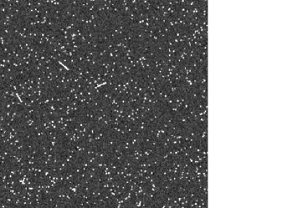
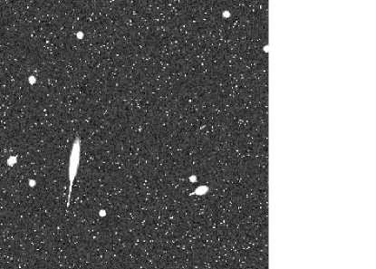
Figure 9 (left panel) shows a simulated frame for a generic (CTI-free) BI device with 1000 1-keV photon events and 10 particle events, assuming the uniform illumination one would expect in subassembly calibrations. Note that most of the photon events are spread among several pixels at this energy because these low-energy photons interact close to the back surface and their charge clouds undergo substantial spreading as they travel many microns through the depletion region toward the gates. For comparison, consider the right panel of Figure 9, which also contains 1000 1-keV photon events and 10 particle events, but detected by a generic FI device. Most of the photon events are contained in a single pixel because shallow interactions in an FI device generate charge clouds that only travel a short distance, thus suffering minimal spreading. Note how much more the particle events have bloomed – this is a result of the thick substrate assumed for this device.
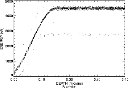
The simulator may optionally attempt to match up photons and events – there is not a one-to-one correspondence due to fluorescence and other effects – and then save for each event the photon’s interaction position in three dimensions. The interaction depths, plotted against event energy, have been very helpful in diagnosing what layer of the device is responsible for certain spectral features in the redistribution function. Figure 10 illustrates this for both FI and BI devices with a simulation of 4.5 keV photons impacting ACIS. The simulated spectra that correspond to these plots are shown in the next section.
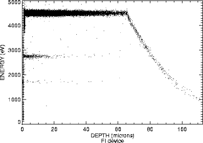
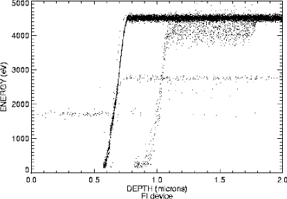
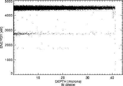
The left panels of Figure 10 show the full range of photon interaction depths. Although most photons interact in the depletion regions of both devices (as designed) and generate events that populate the main photopeak (dark locus of points at 4500 eV in the figure), these plots clearly illustrate the origins of other features in the spectral redistribution function. For example, the locus at 2700 eV comprises the escape peak; the locus at 1740 eV represents fluorescent photon events that populate the fluorescence peak.
In the FI device (top), events lose charge in the bulk field-free substrate (65m and deeper) due to charge spreading and add to the continuum; many of these events will be removed by grade filtering, but some remain in the standard g02346 grades and contribute to the soft shoulder in the spectrum of high-energy photons. The thinned BI device (bottom) has no field-free substrate to contribute to the soft shoulder and the data confirm that this feature is much reduced in BI spectra.
The right panels of Figure 10 show the importance of the gate structure and channel stops in the FI spectral redistribution function and that of the damage and epitaxial layers in the BI spectral redistribution function. Events partially interacting in these surface layers populate the continuum in the spectra and are shown in the depth plots as the steep-sloped components rising from the event detection threshold up to the main peak at 4500 eV. In FI devices, the channel stops are near the illuminated surface of the CCD, so a nontrivial fraction of events interact there and populate the soft shoulder just below the main peak in the spectrum; the top right panel shows these events at interaction depths of 1.1–1.8m. In BI devices, fewer events make it through the entire depth of the device to encounter the channel stops; the lower left panel of Figure 10 shows them at depths of 40–41m. Plots such as these were examined for simulated datasets at a wide range of energies and used to confirm how and channel stop tuning parameters affected the spectral response.
8 Comparing Simulations to Data
To illustrate the performance of the model, below are various examples of simulated output compared to XRCF data. The main comparitors are spectra, quantum efficiency (QE) and grade distributions. In addition, the BI device requires a comparison of simulated and real CTI effects (see the companion paper). Since the FI chips showed minimal CTI at XRCF, we can eliminate this factor when comparing to XRCF data. This allows us to instantiate the CCD model without the confusing effects of CTI, then separately add in CTI effects to reproduce on-orbit data. These FI CTI effects will also be described in detail in the companion CTI paper.
8.1 An ACIS FI Device
Here we compare simulations and XRCF data for the ACIS I3 chip. Data from all four amplifiers are combined. Note that all spectra are presented using log-linear scales; most of the events are contained in the main spectral peak, but most of the insight into the device physics is to be gained by studying the relatively few events that appear at lower energies.
Figure 11 shows a spectrum of 1.383 keV Phase I data with uniform illumination taken on the I3 chip and its corresponding simulation. The low-energy peak is larger in the data than in the simulation because of high-energy continuum photons from the source interacting in the gate structure of the CCD. The simulation models a monochromatic input spectrum at 1.383 keV rather than the actual source spectrum.


Figure 12 gives a spectrum of 4.5 keV Phase I data with uniform illumination taken on the I3 chip and its corresponding simulation. The peak at about 1.2 keV in the data is not reproduced by the simulator because it is due to a Ge L line complex in the source rather than spectral redistribution by the CCD.


Figure 13 illustrates how continuum emission from the XRCF source can contaminate the calibration spectrum. The continuum emission is due to leakage of a bremmsstrahlung continuum through the source filters, which explains why the contamination is preferentially to the soft (low energy) side of the line. The 6.404 keV data show a much larger soft shoulder than the simulation, due to this contamination. Such effects limit our ability to tune the simulator to reproduce subtle spectral redistribution features.


Table 1 compares the grade distributions of the data to the simulated event list for the three example energies given above. Only the standard ASCA grades are listed because contamination from the source continuum causes grades 1, 5, and 7 to be overpopulated in the data. Again, the tuning metric used was the number of g0 events only. The simulator keeps symmetry in the number of right- and left-hand split events (Grades 3 and 4) with respect to the number of up and down split events (Grade 2): g2 g3 + g4. The asymmetry in the data (g2 g3 + g4) could be due to the complicated geometry of the gate structure or channel stops or other effects not contained in the simulations.
| ASCA | 1.383 keV | 4.5 keV | 6.404 keV | |||
|---|---|---|---|---|---|---|
| grade | Data (%) | Simulation (%) | Data (%) | Simulation (%) | Data (%) | Simulation (%) |
| 0 | 81.6 0.4 | 81.3 0.4 | 63.9 0.3 | 63.9 0.3 | 41.6 0.2 | 41.9 0.2 |
| 2 | 10.3 0.2 | 9.2 0.1 | 16.6 0.1 | 15.7 0.1 | 18.8 0.2 | 20.7 0.2 |
| 3 | 3.3 0.1 | 4.2 0.1 | 5.9 0.1 | 7.6 0.1 | 7.3 0.1 | 10.4 0.1 |
| 4 | 3.2 0.1 | 4.3 0.1 | 5.8 0.1 | 7.8 0.1 | 7.3 0.1 | 10.2 0.1 |
| 6 | 1.6 0.1 | 1.1 0.1 | 7.8 0.1 | 5.1 0.1 | 25.0 0.2 | 16.8 0.2 |
The quantum efficiency of the simulator can be measured with vastly less effort than that required to measure the QE of real ACIS devices. Here we use the predicted QE as a way to compare the PSU CCD simulator to the MIT/CSR simulator. For the PSU simulation, a known number of photons are simulated, including CTI and excluding events with grades that are not telemetered by the ACIS instrument, then corrected using our CTI corrector. The resulting events are grade filtered (g02346). Then the number of g02346 events is computed and divided by the number of input photons. This simple definition of QE thus includes events that have been spectrally redistributed out of the main photopeak.
The resulting QE curves, for the bottom and top 128 rows of the I3 FI device at 110C, are shown in Figure 14 along with that reported for the spatially averaged (full-CCD) pre-launch ACIS I3 device by MIT/CSR [11]. The MIT QE curve is calculated from their CCD simulator results, based on the detailed absolute and relative QE measurements made on the ACIS reference and flight CCDs at the BESSY synchrotron and MIT labs [11]. The pointwise deviations in the PSU estimates reflect counting statistics; each point is obtained from simulations of events. The MIT release notes state that the spatial variations of QE were less than 5% for FI devices, but subsequent radiation damage changes this result.


The PSU curve for the bottom of the device (the area least affected by CTI) is useful for comparing to the MIT results; this curve generally falls within the 5% deviations expected for pre-launch devices. We do not tune the layer thicknesses to try to get a specific QE performance from the PSU simulator. The discrepancies between our simulated QE and the MIT results might be due in part to slight differences in our methods for calculating QE or our simplified model of the gate structure. A detailed error analysis of the MIT QE calculation is given in the ACIS Calibration Report [11].
The curve for the top of the device (the area most affected by CTI) clearly deviates from the pre-launch predictions, even after CTI correction. This is because CTI smears the charge distributions, causing events to migrate into grades that are not telemetered to the ground, thus they are not available for CTI correction. This effect is only important for data gathered at a focal plane temperature of 110C (used only in the first few months of the mission). By lowering the temperature to 120C, FI CTI effects were mitigated enough that the FI QE does not exhibit this spatial dependence. We show the 110C simulation here as a warning to users of early ACIS data that the spatial dependence of the QE cannot be ignored.
8.2 An ACIS BI Device
Inherent in the BI simulation is a model for the CTI. Since this is detailed in the companion paper [18], we will not dwell on the CTI model here. Its fidelity does affect the comparison diagnostics presented below, however. Subtle spectral features obvious in FI XRCF data become apparent in BI data when CTI is accounted for, although the origins of such features are not always exactly the same.
Figure 15 (left) gives a spectrum of CTI-corrected 1.383 keV data with uniform illumination taken on a BI chip. On the right is the corresponding simulation of a CTI-free device. Noticeably absent (compared to Figure 11) is the soft shoulder just below the main peak; since the channel stops are far from the illuminated surface on BI devices, fewer events interact there thus the soft shoulder is less populated.


Figure 16 (left) shows a spectrum of CTI-corrected 4.5 keV data with uniform illumination taken on a BI chip, with the CTI-free simulation on the right. As expected, the Ge L complex at about 1.2 keV in the data is not reproduced by the simulator. Although the width of the main peak in the simulation is tuned to match that in the data, the main peak in the data appears to have broader wings than in the simulation. This is probably due to residual CTI effects (e.g. the non-uniform trap distribution results in column-to-column variations in the charge loss; incomplete correction for these variations contributes to wings in the spectral lines).
In spite of the extra artificially added below the gate structure of the device to make a “virtual dead layer” for generating fluorescent photons, we are still underestimating the amplitude of the fluorescence peak at this and higher energies. This implies that the source of these fluorescent photons is not some silicon compound lying below the gate structure in the BI device. Again the rim around the device could be the source, but finding a spatial signature of this effect in the XRCF data is difficult because we don’t have full-frame data for most energies and the photon statistics are quite limited.


Figure 17 confirms our assertion above that continuum emission from the XRCF source is contaminating the calibration spectrum at this energy. The BI 6.404 keV data show a much larger soft shoulder than the simulation due to this contamination, just as the FI data showed (Figure 13).


Table 2 compares the grade distributions of the BI data to the simulated event list. Again, the tuning metric used was the number of g0 events in the main spectral peak. The data show slightly fewer single-split (ASCA grades 2, 3, or 4) events than the simulation and correspondingly more g6 events; the overall match is comparable to the FI examples above.
| ASCA | 1.383 keV | 4.5 keV | 6.404 keV | |||
|---|---|---|---|---|---|---|
| grade | Data (%) | Simulation (%) | Data (%) | Simulation (%) | Data (%) | Simulation (%) |
| 0 | 27.6 0.2 | 27.8 0.2 | 19.5 0.2 | 19.5 0.2 | 24.4 0.3 | 25.2 0.3 |
| 2 | 26.4 0.2 | 25.9 0.2 | 23.0 0.2 | 23.8 0.2 | 20.5 0.3 | 23.0 0.3 |
| 3 | 12.1 0.1 | 13.1 0.1 | 10.0 0.1 | 11.9 0.1 | 8.7 0.2 | 11.3 0.2 |
| 4 | 12.8 0.1 | 12.9 0.1 | 11.3 0.1 | 11.9 0.1 | 9.9 0.2 | 11.2 0.2 |
| 6 | 21.2 0.2 | 20.3 0.2 | 36.2 0.2 | 32.9 0.2 | 36.5 0.4 | 29.3 0.3 |
The BI QE curves, calculated for the same energies and rows as the FI QE curves shown above, are shown in Figure 18 along with that reported for the spatially-averaged (full-CCD) pre-launch ACIS S3 device (with no CTI correction) by MIT/CSR [11]. Again the pointwise deviations in the PSU estimates reflect counting statistics; events per energy were simulated to calculate the QE. The MIT release notes state that there are spatial variations in the BI QE of up to 20% [11]; this must be due at least in part to CTI effects.


The PSU curve for the bottom of the device (the area least affected by parallel CTI) matches the MIT curve above 3.5 keV fairly well, where surface effects are minimized. Serial CTI effects dominate in this spatial region but don’t cause enough grade morphing that events are lost to on-board grade filtering. The top of the device is the area most affected by the combined effects of parallel and serial CTI. The QE curve here clearly deviates from the pre-launch predictions, even at high energies and after CTI correction. This is again because CTI caused events to morph into grades that are not telemetered to the ground, thus they are not available for CTI correction.
Our model shows significant deviation from MIT’s in the BI QE below the oxygen absorption edge (543 eV), for both the top and bottom of the device (note that we only calculate QE down to 0.2 keV but the MIT curve continues to lower energies). CTI effects are not large at low energies on BI devices (e.g. the two PSU QE curves converge), so grade morphing can’t explain these QE deviations. Perhaps differences in the way the two groups model the dead and damage layers first encountered by photons impinging on the BI device are causing these variations in the model QE.
9 Applications
9.1 Response Matrices
The CCD spectral redistribution function is encapsulated for the purposes of spectral fitting in a “response matrix” [11], where each row corresponds to the spectral response of the device (in DN) at a given input monochromatic energy (in eV). We have used our Monte Carlo CCD simulator to generate response matrices appropriate for CTI-corrected on-orbit data. The simulator is used to generate event lists at a very large number of monochromatic energies spanning the range of interest for Chandra observations (0.2 – 10 keV). These event lists are filtered to remove events that would not have been telemetered by the real ACIS instrument and the remaining events are CTI-corrected using the PSU corrector. The resulting spectral redistribution functions form the rows of the response matrix.
The response matrix generator for FI devices accepts a range of CCD row numbers as input, so the user may create a matrix applicable to extended structures as well as point sources located anywhere on the device. This is necessary because the PSU CTI corrector cannot compensate for the CTI-induced energy resolution degradation on FI devices [18], so position-dependent response matrices are still needed to analyze some ACIS celestial spectra. Since the BI CTI is less severe, this position-dependent spectral resolution is not seen in BI data and a single response matrix is adequate for fitting pointlike or extended structures anywhere on a BI CCD.
An example FI matrix, generated for the aimpoint of the ACIS imaging array at a focal plane temperature of 110C (where the spectral broadening is at its worst), is shown in Figure 19. The main peak is represented by the dark diagonal locus. The grey smear to the left of the main peak locus is the soft shoulder, produced by photons interacting in the channel stops. At low energies photons interact near the surface of the device and populate the low-energy tail. The escape peak tracks the main peak and doesn’t appear until the input photon energy is above the Si absorption edge of 1839 eV. This edge represents a sharp reduction in the transmissivity of so more events interact near the surface of the device, repopulating the soft shoulder and low-energy tail; thus the grey smear below the main peak reappears at 1839 eV and slowly dies off at higher energies, as photons interact deeper in the device. The Si fluorescence peak becomes populated above the Si absorption edge and appears as a vertical locus of points in the matrix. Above 4 keV, the spectral redistribution features due to the surface layers of the device have died away and the main and escape peaks are noticeably broadened by the intrinsic spectral resolution of the device.
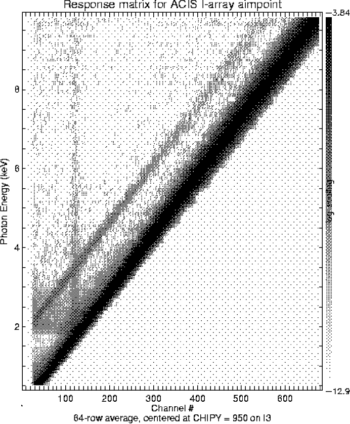
This method for generating response matrices involves creating a large database of simulated events, then accessing a subset of those events relevant to the spectral analysis task at hand. A natural result of this design is that the event database can be filtered for other properties in addition to location on the CCD, such as event grade, so the user can tailor a matrix to the specific science goals of the observation. For example, higher spectral resolution and background rejection may be obtained by keeping just ASCA Grade 0 or Grade 0, 2, 3, and 4 events, rather than the standard “g02346” grade set. Brandt et al. [37] used such a restricted grade set to improve the signal-to-noise of faint source detections in the Chandra Deep Field North. See also Chartas et al. [38] for a more detailed explanation of special filtering for optimizing aspects of ACIS data.
Another distinction of this method from typical techniques is that the spectral redistribution function (the output of the simulator) is recorded directly as a row in the matrix. Since the simulator does not produce an infinite number of events, the resulting matrix is not perfectly smooth; this is apparent in Figure 19. Other techniques involve parameterizing the simulated spectra by fitting a set of Gaussians or other functional forms then storing the fit parameters. This produces a very compact format for storing the response matrix and removes the stochastic nature inherent in our technique, but its fidelity is limited by the quality of the fits to the simulated data, in addition to any errors introduced by the simulation itself.
9.2 Fitting the External Calibration Source Spectrum
We used the above response matrix to fit a spectrum from the External Calibration Source (ECS), including only events from the 100 rows surrounding the ACIS Imaging Array aimpoint on the I3 chip. There are CTI-corrected events in this spectrum. Because of CTI, this region has the worst spectral resolution on the device, but it is important to do spectral modeling here because it has the best spatial resolution, so many targets are imaged at this location. The main spectral features included in the fit are listed in Table 3 along with the line energies recovered by the XSPEC [39] fit. The actual fit is shown in Figure 20.
| Spectral line | True energy (eV) | Fit energy (eV) | Normalization | |
|---|---|---|---|---|
| Mn/Fe L complex | 680 | fixed | 0.05 (fixed) | 212 46 |
| Al K | 1486 | 1495 1 | 0.00 | 75334 376 |
| Si K | 1740 | fixed | 0.06 | 2271 106 |
| Au M complex | 2112 | fixed | 0.19 | 869 71 |
| Ti K escape | 2771 | N/A | N/A | N/A |
| uncertain | uncertain | 3655 27 | 0.14 | 364 49 |
| Mn K escape | 4155 | N/A | N/A | N/A |
| Ti K | 4511 | 4501 1 | 0.05 | 73142 677 |
| Ti K | 4932 | 4899 7 | 0.10 | 13415 519 |
| Mn K | 5895 | 5874 1 | 0.05 | 233450 528 |
| Mn K | 6490 | 6432 4 | 0.14 | 41599 505 |
| Mn K + Al K pileup | 7381 | 7330 38 | 0.17 | 529 72 |
| Au L | 9711 | fixed | 0.11 | 177 37 |

The lines marked as “uncertain” may be Ca K (3.69 keV) or the escape peak of Cr K (3.67 keV) (Allyn Tennant, private communication). The spectrum contains some background as well as the emission lines. This background has a complicated spectral shape but is modeled here as a simple power law of photon index 0.720.04 (normalization 120666).
The fit had a for 281 degrees of freedom; this would be unacceptably large for a fit to a typical astrophysical spectrum but is not unreasonable for this calibration spectrum made from such a large number of events. We suspect that more sophisticated modeling of the background would improve ; it may also be large because the spectral lines were modeled as Gaussians when in fact they have noticeably non-Gaussian wings. These wings are due to residual CTI effects; gain variations that were not removed by the CTI corrector are by definition not incorporated into the CTI model that was used to generate the response matrix, so to account for this completely the spectral line model would require broader wings.
This non-Gaussian line shape may also explain why the fit energies of the Ti and Mn K lines are low. The K lines are blended with the non-Gaussian wings of their K counterparts, which may skew the K Gaussian fit toward lower energies. By choosing to fit data taken at -110C (where CTI is most pronounced) and concentrating on the section of the device farthest from the readout nodes (where the stochastic nature of CTI results in the largest gain variations), we have maximized this effect.
The bright lines contain so many events that the errors on the fit energies are extremely small. Conversely, the limited counts in the weak lines caused those lines to be poorly constrained in the fit. To account for this, sometimes their line energies and widths were fixed before the fit was performed. The table notes which lines were constrained. Escape peaks from Ti K and Mn K are prominent in the spectrum. They were not modeled as independent Gaussians; rather their amplitudes, widths, and line centers follow from the spectral redistribution function instantiated in the response matrix.
9.3 The LYNX Pile-up Simulator
Chartas et al. have developed the spectral fitting tool LYNX [40] that employs a forward fitting approach to infer incident astrophysical flux and spectra by interfacing the standard X-ray spectral fitting package XSPEC [39] to the raytrace code MARX [25] and this CCD simulator. Astrophysical spectra obtained with ACIS are initially fit with XSPEC to provide starting estimates of the spectral parameters for LYNX. The modeled incident spectrum is propagated through the Chandra mirrors with MARX, through the ACIS Optical Blocking Filters via their X-ray transmission function [41], then to the CCD simulator to become instantiated into events. A merit function that incorporates the differences between the observed and simulated spectra is minimized using a downhill simplex method to yield the best-fit model parameters.
The CCD simulator allows LYNX to account for the possible overlap of the resulting charge clouds within each exposure, thus the spectra produced through LYNX will simulate pile-up. The present version of LYNX also allows spectral fitting using any grade selection, corrects for telescope vignetting, and accounts for the dither motion of the source across the CCD. A simple example is given below, to illustrate the power of this forward modeling scheme and to show some of the effects of pile-up on ACIS results.
A set of simulated observations was produced for a point source placed at the aimpoint of the S3 chip. The incident spectrum was an absorbed power law with spectral slope = 1.8, modified by Galactic absorption from neutral hydrogen with column density NH = cm-2. The incident count rates (all grades included) ranged between 0.05 counts per frame and 2 counts per frame. The standard full-CCD frametime of 3.24 seconds was used.
Figure 21 shows the effect of photon pile-up on the measured event rate. Even sources of moderate brightness (0.2–0.4 counts per frame) will have 10% errors in their flux estimates if pile-up is not considered. Naive flux estimates for bright sources are substantially in error. Note that this plot assumes that all events are included; grade filtering makes these flux errors even worse, as pile-up causes events to migrate into non-standard grades.

Pile-up also compromises spectral fitting, as shown in Figure 22. This gives the best fit values of obtained with LYNX and XSPEC as a function of the observed counts per frame. Here the observed counts per frame include only events with energies lying between 0.2 and 10 keV and all grades. For fits performed with XSPEC we used standard grade selection and the standard response matrices and ancillary files for the BI device S3 provided by the CXC.

Above 0.2 counts per frame the pile-up effect produces noticeably flatter spectra. LYNX is able to recover the incident spectral slope for observed rates of up to 0.7 counts per frame. This observed rate corresponds to an incident rate of 1 count per frame. We are experimenting with improving the performance of LYNX at even higher count rates by removing the grade filter that was applied in the spectral fitting (Chartas et al., in preparation).
10 Summary and Further Work
10.1 Simulator Status
The current model reproduces all the main features in ACIS calibration spectra for both FI and BI devices. The grade distributions are reproduced to within a few percent, after the simulator is tuned to yield the correct percentage of Grade 0 events. We compare the output of our simulator to that of the MIT/CSR CCD simulator via the quantum efficiencies of both FI and BI devices. They are consistent to within the errors at most energies, although the errors quoted are large.
We must employ tuning parameters to account for physics that we have not explicitly incorporated in the theory. The model predicts the device response at new energies by linearly interpolating the tuning parameters determined from calibration data. At some energies, the quality of the tuning parameters is limited by the quantity and quality of data available.
The PSU simulator borrows many basic features and physical quantities from the MIT/CSR simulator, so the QE consistency is not surprising. The MIT/CSR simulator employs a much more detailed model of the gate structure and channel stops, but our simpler slab model seems adequate to reproduce the spectral features seen in XRCF data. These two ACIS simulators share no code and were tuned on independent datasets (sub-assembly vs. XRCF), so they provide useful checks for each other – the similarity of their output gives us confidence in their fidelity and in the stability of the ACIS CCDs.
Our simulator is capable of modeling epitaxial FI devices and some limited testing has been performed for such devices, but the code has not been tuned to reproduce an actual laboratory device. Similarly, the code exists to model minimally-ionizing particle interactions, but no detailed comparison to actual particle events has been undertaken.
To facilitate independent assessment of our modeling techniques, the simulator source code and a Users’ Manual are available for use by the community222http://www.astro.psu.edu/users/townsley/simulator/. Further implementation details and assumptions made are described there. We welcome input from other CCD modelers and astronomers interested in ACIS device calibration and simulation.
10.2 Future Work
One clear extension of this work is to replace the point-wise interpolation of tuning parameters with models. This should be straightforward at energies far from the important absorption edges of O, N, and Si, but care must be taken to avoid oversimplifying the tuning parameter behavior in these regions. Our values for the tuning parameters are affected by the XRCF and flight data used to tune them, so modeling them might remove some of the simulator’s dependence on the quality of these data. It is likely that such modeling will yield more insight into the device physics that is manifested as spectral redistribution features.
We have generated response matrices for ACIS FI devices I0–I3, S2, and S4 using the simulator tuning parameters derived for I3 (except for the CTI-induced, row-dependent spectral resolution, which was tuned for each device). This was mandated by lack of time and resources and justified by MIT’s subassembly calibration, which showed that all FI devices were quite similar prior to launch. If these matrices are shown to be inadequate for spectral fitting of celestial sources due to inaccurate modeling of the spectral redistribution function (rather than, say, CTI effects), one course of action would be to return to the XRCF data and tune the simulator for each FI device. This would be a labor-intensive undertaking.
Further refinements to the simulator might be necessary to achieve adequate modeling of other devices for other missions. We usually include physical models in response to the demands of the data rather than by presupposing the relevance of a physical process, since there are so many such processes at work in these detectors. Given that, CCDs of substantially different design (such as very thin BI devices or FI devices with radically different gate structures) may require the invocation of new physics in a future simulator.
Despite its limitations, the current incarnation of the full-frame simulator is useful for addressing timely issues in CCD characterization. The code has been used to develop an algorithm to determine sub-pixel positions of photons [11] and to assess the problems associated with photon pile-up from bright point sources [42]. It has been used in conjunction with SAOSAC and MARX to model the Chandra point spread function at XRCF [11]. Event lists generated by this simulator are being used to generate ACIS response matrices for X-ray spectral analysis of celestial sources.
A product of our work on the CTI corrector is the ability to include some of the effects of CTI in the CCD simulator, namely grade migration and event energy degradation as a function of position on the device. We have additionally included another noise term in the simulator to account for the spectral line broadening caused by charge traps (see the accompanying paper [18] for details). These features of the model allow us to reproduce on-orbit ACIS calibration data for both FI and BI CCDs. Second-generation tools such as LYNX are combining the power of XSPEC, MARX, and the CCD simulator to model astrophysical spectra affected by pile-up. Armed with these simulation tools, we are prepared to face the challenge of modeling Chandra/ACIS celestial data.
References
- [1] S. L. O’Dell, M. C. Weisskopf, Advanced X-ray Astrophysics Facility (AXAF): Calibration overview, in: X-Ray Optics, Instruments, and Missions, Vol. 3444, SPIE, 1998, p. 2.
- [2] M. C. Weisskopf, H. D. Tananbaum, L. P. V. Speybroeck, S. L. O’Dell, Chandra X-ray Observatory (CXO): Overview, in: International Symposium on Astronomical Telescopes and Instrumentation 2000, Vol. 4012, SPIE, 2000, p. 2.
- [3] G. P. Garmire, J. A. Nousek, M. W. Bautz, ApJ in preparation.
- [4] The Chandra X-ray Center, Chandra Proposers’ Observatory Guide, available at http://asc.harvard.edu/udocs/docs/docs.html (March 2000).
- [5] D. H. Lumb, G. D. Berthiaume, D. N. Burrows, G. P. Garmire, J. A. Nousek, Charge coupled devices (CCDs) in X-ray astronomy, Experimental Astronomy 2 (1991) 179.
- [6] B. Burke, J. Gregory, M. Bautz, G. Prigozhin, S. Kissel, B. Kosicki, A. Loomis, D. Young, Soft X-ray CCD imagers for AXAF, IEEE Trans. Electron. Devices 44 (10).
- [7] G. Prigozhin, A. Rasmussen, M. Bautz, G. Ricker, A model of the X-ray response of the ACIS CCD, in: X-Ray Optics, Instruments, and Missions, Vol. 3444, SPIE, 1998, p. 267.
- [8] M. Pivovaroff, S. Kissel, M. Bautz, G. Prigozhin, T. Isobe, J. Woo, J. Gregory, Flight X-ray CCD selection for the AXAF CCD Imaging Spectrometer, in: EUV, X-Ray, and Gamma-Ray Instrumentation for Astronomy VII, Vol. 2808, SPIE, 1996, p. 182.
- [9] M. Bautz, M. Pivovaroff, F. Baganoff, T. Isobe, S. Jones, S. Kissel, B. LaMarr, H. Manning, G. Prigozhin, G. Ricker, J. Nousek, C. Grant, K. Nishikida, F. Scholze, R. Thornagel, G. Ulm, X-ray CCD calibration for the AXAF CCD Imaging Spectometer, in: X-Ray Optics, Instruments, and Missions, Vol. 3444, SPIE, 1998, p. 210.
- [10] J. A. Nousek, G. P. Garmire, Science instrument operations handbook for the AXAF CCD Imaging Spectrometer, NASA Document ACIS-PSU-SOP-01, The ACIS Instrument Team, available at www.astro.psu.edu/xray/axaf/ (November 1997).
- [11] M. W. Bautz, J. A. Nousek, G. P. Garmire, Calibration report for the AXAF CCD Imaging Spectrometer, Tech. rep., The ACIS Instrument Team, available at www.astro.psu.edu/xray/axaf/ (January 1999).
- [12] M. Bautz, G. Prigozhin, M. Pivovaroff, S. Jones, S. Kissel, G. Ricker, X-ray CCD response functions, front to back, Nucl. Instr. and Meth. in Phys. Res. A 436 (1999) 40.
- [13] G. Prigozhin, S. Jones, M. Bautz, G. Ricker, S. Kraft, The physics of the low energy tail in the ACIS CCD. The spectral redistribution function, Nucl. Instr. and Meth. in Phys. Res. A 439 (2000) 582.
- [14] K. Hayashida, S. Kitamoto, E. Miyata, H. Tsunemi, K. Yoshita, T. Kohmura, K. Mori, K. Katayama, H. Katayama, M. Shouho, M. Ohta, T. Dotani, M. Ozaki, K. Koyama, H. Awaki, T. G. Tsuru, G. Ricker, M. W. Bautz, R. Foster, S. Kissel, X-ray imaging spectrometers for Astro-E: Ground calibration in soft X-ray range, in: International Symposium on Astronomical Telescopes and Instrumentation 2000, Vol. 4012, SPIE, 2000, p. 123.
- [15] G. Prigozhin, S. Kissel, M. Bautz, C. Grant, B. L. an d R. Foster, G. Ricker, Characterization of the radiation damage in the Chandra X-ray CCDs, in: International Symposium on Optical Science and Technology 2000, Vol. 4140, SPIE, 2000, p. 123.
- [16] J. E. Hill, K. T. Lewis, R. F. Foster, M. Bautz, S. K. Brown, P. W. A. Roming, A. E. Hornschemeier, D. N. Burrows, G. P. Garmire, A simulation of the flight experience of the ACIS CCDs on the Chandra X-ray observatory, in: International Symposium on Astronomical Telescopes and Instrumentation 2000, Vol. 4012, SPIE, 2000, p. 402.
- [17] L. K. Townsley, P. S. Broos, G. P. Garmire, J. A. Nousek, Mitigating charge transfer inefficiency in the Chandra X-ray Observatory Advanced CCD Imaging Spectrometer, ApJ 534 (2000) L139.
- [18] L. K. Townsley, P. S. Broos, J. A. Nousek, G. P. Garmire, Modeling charge transfer inefficiency in the Chandra Advanced CCD Imaging Spectrometer, Nucl. Instr. and Meth. in Phys. Res. A, in press.
- [19] J. Hill, The charge coupled device as an X-ray polarimeter, Ph.D. thesis, Department of Physics and Astronomy, University of Leicester, Leicester, UK (1999).
- [20] K. J. McCarthy, A. Owens, A. D. Holland, A. A. Wells, Modelling the X-ray response of charge coupled devices, Nucl. Instr. and Meth. in Phys. Res. A 362 (1995) 538.
- [21] A. D. Holland, A. D. T. Short, G. W. Fraser, M. J. L. Turner, The X-ray polarisation sensitivity of CCDs, Nucl. Instr. and Meth. in Phys. Res. A 355 (1995) 526.
- [22] D. H. Lumb, J. A. Nousek, Energy response of astronomical CCD X-ray detectors, in: X-Ray Detector Physics and Applications, Vol. 1736, SPIE, 1992, p. 138.
- [23] G. Pavlov, J. Nousek, Charge diffusion in CCD X-ray detectors, Nucl. Instr. and Meth. in Phys. Res. A 428 (1999) 348.
- [24] D. Jerius, M. Freeman, T. Gaetz, J. P. Hughes, W. Podgorski, The SAO AXAF simulation system, in: Astronomical Data Analysis Software and Systems IV, Vol. 77, ASP, 1995, p. 1.
- [25] M. W. Wise, J. E. Davis, D. P. Huenemoerder, J. C. Houck, D. Dewey, K. A. Flanagan, C. Baluta, The MARX 2.0 User Guide, The Chandra X-ray Center, available at http://chandra.harvard.edu (October 1997).
- [26] W. H. Press, S. A. Teukolsky, W. T. Vetterling, B. P. Flannery, Numerical Recipes in C: The Art of Scientific Computing, 2nd Edition, Cambridge University Press, 1992.
- [27] G. R. Hopkinson, Charge diffusion effects in CCD X-ray detectors I. Theory, Nucl. Instr. and Meth. in Phys. Res. A 216 (1983) 423.
- [28] J. Janesick, T. Elliott, S. Collins, T. Daud, D. Campbell, A. Dingizian, G. Garmire, CCD advances for X-ray scientific measurements in 1985, in: X-Ray Instrumentation in Astronomy, Vol. 597, SPIE, 1985, p. 364.
- [29] J. R. Janesick, T. Elliott, S. Collins, T. Daud, D. Campbell, G. Garmire, Charge-coupled device advances for X-ray scientific applications in 1986, Optical Engineering 26 (1987) 156.
- [30] G. R. Hopkinson, Analytic modeling of charge diffusion in charge-coupled-device imagers, Optical Engineering 26 (1987) 766.
- [31] C. Jacoboni, C. Canali, G. Ottaviani, A. A. Quaranta, A review of some charge transport properties of silicon, Solid-State Electronics 20 (1977) 77.
- [32] A. Yamashita, Master’s thesis, University of Tokyo (1995).
- [33] G. Prigozhin, J. Woo, J. Gregory, A. Loomis, M. Bautz, G. Ricker, S. Kraft, X-ray absorption near edge structure in quantum efficiency of X-ray CCDs, Optical Engineering 37 (10) (1998) 2848.
- [34] B. L. Henke, E. M. Gullikson, J. C. Davis, X-ray interactions: Photoabsorption, scattering, transmission, and reflection at E=50–30,000 eV, Z=1–92, Atomic Data and Nuclear Data Tables 54 (2) (1993) 181.
- [35] J. Nousek, L. Townsley, G. Chartas, D. Burrows, E. Moskalenko, R. Sambruna, J. Pesce, C. Grant, K. Nishikida, L. Cawley, P. Broos, T. S. Koch, A. Garmire, G. Garmire, M. Bautz, S. Jones, B. L. Marr, G. Ricker, Joint AXAF High-Resolution Mirror Assembly and AXAF CCD Imaging Spectrometer calibration at the MSFC X-ray Calibration Facility, in: X-Ray Optics, Instruments, and Missions, Vol. 3444, SPIE, 1998, p. 225.
- [36] Research Systems Inc., IDL, the Interactive Data Language, IDL, Copyright (1998).
- [37] W. N. Brandt, A. E. Hornschemeier, D. M. Alexander, G. P. Garmire, D. P. Schneider, P. S. Broos, L. K. Townsley, M. W. Bautz, E. D. Feigelson, R. E. Griffiths, The Chandra deep survey of the Hubble Deep Field North Area. IV. An ultradeep image of the HDF-N, AJ 122 (2001) 1.
- [38] G. Chartas, G. Garmire, J. Nousek, S. Koch, S. Kissel, G. Prigozhin, M. Bautz, Optimizing the ACIS effective area and energy resolution, in: Symposium on Optical Science, Engineering and Instrumentation, Vol. 3444, SPIE, 1998, p. 258.
- [39] K. A. Arnaud, XSPEC: The first ten years, in: Astronomical Data Analysis Software and Systems V, Vol. 5, ASP Conf. Ser. 101, 1996, p. 17.
- [40] G. Chartas, D. M. Worrall, M. Birkinshaw, M. Cresitello-Dittmar, W. Cui, K. K. Ghosh, D. E. Harris, E. J. Hooper, D. L. Jauncey, D.-W. Kim, J. Lovell, S. Mathur, D. A. Schwartz, S. J. Tingay, S. N. Virani, B. J. Wilkes, The Chandra X-ray observatory resolves the X-ray morphology and spectra of a jet in PKS 0637-752, ApJ 542 (2000) 655.
- [41] G. Chartas, G. P. Garmire, J. A. Nousek, L. K. Townsley, F. R. Powell, R. L. Blake, D. E. Graessle, ACIS UV/optical blocking filter calibration at the National Synchrotron Light Source, in: Multilayer and Grazing Incidence X-ray/EUV Optics III, Vol. 2805, SPIE, 1996, p. 44.
- [42] P. S. Broos, L. K. Townsley, J. A. Nousek, Discarding piled-up events in ACIS, in: X-Ray Optics, Instruments, and Missions, Vol. 3444, SPIE, 1998, p. 30.