Recent Progress in CdTe and CdZnTe Detectors
Abstract
Cadmium telluride (CdTe) and cadmium zinc telluride (CdZnTe) have been regarded as promising semiconductor materials for hard X-ray and -ray detection. The high atomic number of the materials (ZCd =48, ZTe=52) gives a high quantum efficiency in comparison with Si. The large band-gap energy (Eg 1.5 eV) allows us to operate the detector at room temperature. However, a considerable amount of charge loss in these detectors produces a reduced energy resolution. This problem arises due to the low mobility and short lifetime of holes. Recently, significant improvements have been achieved to improve the spectral properties based on the advances in the production of crystals and in the design of electrodes. In this overview talk, we summarize (1) advantages and disadvantages of CdTe and CdZnTe semiconductor detectors and (2) technique for improving energy resolution and photopeak efficiencies. Applications of these imaging detectors in future hard X-ray and gamma-ray astronomy missions are briefly discussed.
Index Terms:
CdTe, CdZnTe, CZT, gamma-ray, Pixel Detector.I Introduction
There are increasing demands for new semiconductor detectors capable of detecting hard X-ray and -rays. For imaging devices, their good energy resolution and the ability to fabricate compact arrays are very attractive features in comparison with inorganic scintillation detectors coupled to either photodiodes or photomultiplier tubes.
Despite the excellent energy resolution and charge-transport properties of silicon (Si) and germanium (Ge) detectors, their low stopping power for high energy photons limits their application to hard X-ray and -ray detection. Furthermore, the small band gap of germanium forces us to operate the detector at cryogenic temperatures. Therefore, room-temperature semiconductors with high atomic numbers and wide band gaps have long been under development. These materials are useful not only in medical and industrial imaging systems but also in detectors for high energy particle- and astrophysics.
Cadmium Telluride (CdTe) has been regarded as a promising semiconductor material for hard X-ray and -ray detection since the early 1970’s. The high atomic number of the materials gives a high quantum efficiency suitable for a detector operating typically in the 10500 keV range. A large band-gap energy ( = 1.44 eV) allows us to operate these detectors at room temperature. However, it became clear that it would be much more difficult to use CdTe in comparison with Si and Ge, especially for nuclear spectroscopy, where good spectroscopic performance is desired. The lack of stability also limited the usefulness of CdTe detectors in the past. Problems and efforts to improve the properties of CdTe detectors since its beginning are available in review articles[1, 2].
In the 1990’s, the remarkable progress in the technology of producing a high quality single crystal of CdTe and the emergence of Cadmium Zinc Telluride (CdZnTe) have dramatically changed the situations of high resolution room temperature detectors [3]. Furthermore, advances in application specific integrated circuits (ASICs) leads to fabrication of position sensitive detectors in the form of strip or pixellated detectors[4, 5]. Here we summarize the recent progress of the development of CdTe and CdZnTe detectors.
II CdTe and CdZnTe semiconductor
| semi- | density | Z | |||
|---|---|---|---|---|---|
| conductor | [eV] | [eV] | [cm] | ||
| Si | 2.33 | 14 | 1.12 | 3.6 | 9.37 |
| Ge | 5.33 | 32 | 0.67 | 2.9 | 2.30 |
| CdTe | 5.85 | 48,52 | 1.44 | 4.43 | 1.52 |
| CdZnTe | 5.81 | 1.6 | 4.6 | ||
| 6.40 | 80,53 | 2.13 | 4.2 | 1.16 | |
| 5.32 | 31, 33 | 1.42 | 4.3 | 2.29 |
| : | band gap energy | |
| : | an ionization potential | |
| : | radiation length |

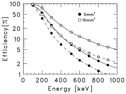
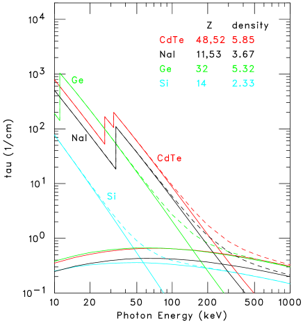
Table I shows the physical characteristics of the elemental and compound semiconductors. Among the range of semiconductor detectors available for -ray detection, CdTe (and CdZnTe) have a privileged position[6, 7, 8], because of their high density and the high atomic number of their components, as well as a wide bandgap. As shown in Fig. 1 , CdTe has a high photoelectric attenuation coefficient. Photoelectric absorption is the main process up to 300 keV for CdTe, as compared to 60 keV for Si and 150 keV for Ge. Fig. 2 shows the efficiency for 100 keV -rays. Even a detector with a thickness of 0.5 mm provides a good detection efficiency for -rays. Efficiencies calculated with a simulation code [9] are shown in Fig. 3 for a detector with a thickness of 5 mm and 10 mm. For a 511 keV photon, an absorption efficiency of 15.5% can be obtained for a 10 mm cube detector. These efficiencies, however, assume that -ray photons deposit all their energy in the detector volume and that we can collect all electron-hole pairs generated in the detector. It has been pointed out that the considerable amount of charge loss in CdTe and CdZnTe limits their capability as high resolution spectrometers[2]. As shown later, this problem is due mainly to the poor charge transport properties, especially for holes. Incomplete charge collection could limit the thickness and, thus, the volume of detectors which in turn limits the usefulness of the detector.
II-A HPB-grown CdZnTe
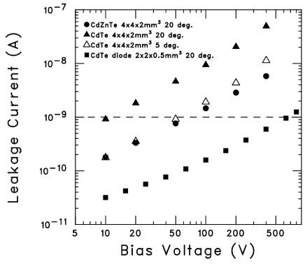
Very recently, Cd1-xZnxTe grown by the High Pressure Bridgman (HPB) technique has emerged as a new choice for room temperature detectors[10, 11, 12]. By increasing theZn concentration, the bandgap of the material is increased from 1.44 eV (for CdTe) to 2.2 eV (for ZnTe)[13]. With the most widely used composition of = 0.08 0.15, CdZnTe has a bandgap of 1.6 eV and displays high electrical resistivity (1.0 4.0) 1010 cm (n-type), which is close to the theoretical maximum allowed by the bandgap[12]. As shown in the current voltage (I-V) characteristics (Fig. 4 ), the leakage current of a 442 mm3 CdZnTe detector is 4 nA at 20 . The low leakage current due to the high resistivity of HPB-grown CdZnTe and its good electron transport of = (0.5 5.0) cm2/V, where is mobility-lifetime product, results in good spectral performance when operated at room temperature. These advantages over conventional CdTe have lead to the early success of small volume single-element planar detectors and simple multi-electrode CdZnTe devices have stimulated more advanced application in a variety of fields[14, 16]. Nevertheless, there are a few drawbacks associated with this new detector material. Although the ingots are of very large volume, the present HPB technique yields only polycrystals with a non-uniform distribution of products. The IR transmission image of the large wafer shows grain boundaries and a distribution of Te-decorated features [17]. Extensive studies indicate that the grain boundaries decorated with Te inclusions or twin boundaries have an adverse effect on carrier transport in CdZnTe and result in poor spectral response[14, 17, 15]. At present, the yield of HPB CdZnTe dies suitable for the fabrication of large-area ( 10 10 mm2) X- and -ray imaging devices is very low [14]. Additionally, the products of holes in CdZnTe detectors is 210-5 cm2/V and is almost one order of magnitude smaller than that of the recent CdTe detector. This is probably due to some degradation in properties introduced by adding Zn.
II-B THM-grown CdTe
After continuous efforts for more than two decades to improve the performance of CdTe crystals, the technique for growing a large single CdTe crystal with good charge transport properties seems to be established[18] CdTe is usually grown by the Traveling Heater Method (THM). After careful thermal treatment and the selection of proper crystal orientation for the electrode system, it is reported that the CdTe wafer displays good charge transport properties for both electrons ( = 12 cm2/V ) and holes ( = 1 cm2/V ). The electrical resistivity of 1109 cm (p-type) is achieved by compensating the native defects with Cl. Furthermore, with the usual electrode configuration with Pt which forms Ohmic contacts, the detector is free from problems with the stability[18]. There are no grain boundaries nor a distribution of Te inclusion in a wafer, since it is a single crystal[17]. The uniform charge transport properties of the wafer are very important aspect not only for fabricating large area strip or pixel detectors but also for constructing a large scale -ray camera with many individual detectors. Single crystals of 50 mm diameter are now commercially available for THM-CdTe. The grown crystal is large enough to obtain (1 1 1)- oriented single crystal wafers with an area as large as 30 30 mm2. A similar approach to growing high quality CdTe single crystals is reported with THM [19] and in a conventional vertical Bridgman furnace[14].

II-C Energy spectra of CdTe and CdZnTe
Because of the very high resistivity, CdTe and CdZnTe are regarded as semi-insulating materials and usually operated as a “solid ionization chamber”[23]. The electron-hole pairs generated in the detector are collected by applying an appropriate bias voltage. Figs. 5 (a) and (b) show the energy spectra of -rays from 57Co obtained at 20 with the CdTe and CdZnTe detectors used in the measurement of the I-V curve (Fig. 5 ). In the measurement, the charge signal is integrated in the Clear Pulse CP-5102 CSA and shaped by an ORTEC 571 amplifier. The time constant of the shaping amplifier was set at 0.5 s for both detectors. In order to minimize the effect of the incompleteness of the hole collection, we irradiated -rays from radioactive sources on the negative electrode (cathode). The applied bias voltages are chosen to be 100 V for the CdTe and 300 V for the CdZnTe detector so that we obtain the comparable leakage current. The energy resolution (FWHM) of the 122 keV line is 6.9 keV for the CdTe detector and 4.2 keV for CdZnTe.
III Effects of low transport of holes
Collecting full information due to the transit of both electrons and holes is important for obtaining the ultimate energy resolution from the device. The mean drift path of the charge carrier is expressed as the product of and , where is the applied electric field in the device. Due to the slow mobility and short lifetime of holes, the thickness of the detector should be smaller than , where and are the mobility and lifetime of holes. If a detector with a thickness is used, only a fraction of the generated signal charge is induced at the detector electrode. The fraction and the resultant pulse height depend on the interaction depth. This position dependency produces a shoulder (tailing) in the peaks of -ray lines towards the low energy region, which is seen in 57Co spectra with CdTe and CdZnTe shown in Fig. 5 . Due to a distortion of the spectrum. The energy resolution does not reach the theoretical limit expected from statistical fluctuations in the number of electron-hole pairs and the Fano factor.
The pulse height as a function of the depth of interaction for a simple planar detector is given by the Hecht equation[20]:
| (2) | |||||
where is the number of electron-hole pairs generated in the detector and is the detector thickness. The depth, is measured from the cathode. The reduction of the pulse height is severe for the event which takes place close to the anode electrode of a 2 mm thick detector, where the signal is mostly due to the hole transit. Only 16% of the signal is collected for = 210-5 cm2/V (typical number for the recent HPB-grown CdZnTe detectors) as compared to the case for with a bias voltage of 300 V. This effect is clearly seen in the 241Am spectrum shown in Fig. 6 which was obtained with a CdZnTe detector with a thickness of 2 mm. When the detector is irradiated by -rays from the cathode face, -ray peaks are clearly resolved. The energy resolution at 60 keV is 3.3 keV. However, if we irradiate -rays from the anode face, the peak structure is smeared out completely. The situation is slightly better for CdTe which has higher , but the spectral performance is still limited.


Many methods have been proposed and used to overcome the hole-trapping problem. One approach is to use the information contained in the pulse shape[2]. In this approach, the pulses with a slow rise time are corrected or discriminated by means of specially designed electronics. A model of the pulse shape is described in [21]. Another approach is the use of a hemispheric geometry [2]. A logarithmetic field inside the detector enhances the collection of fast-moving electrons and restrain the hole collection. The application of hemispheric CdTe and CdZnTe detectors to safeguards measurements are described in [22]
IV High resolution CdTe diode and its application to the stack detector
The theoretical energy resolution of CdTe can be calculated from statistical fluctuations in the number of electron-hole pairs and the Fano factor ()[23]. By using = 4.5 eV and = 0.15, the theoretical limit (FWHM) is 200 eV at 10 keV, 610 eV at 100 keV, and 1.5 keV at 600 keV [30], if we could neglect electronic noise. These resolutions are very attractive for applications in astrophysics, where precise determinations of the central energy and the profile of X-ray and -ray lines are crucial[24]. For obtaining the ultimate energy resolution from the CdTe and CdZnTe detectors, collecting full information given by the transit of both electrons and holes is important. Fig. 7 is the result of simulations showing that high bias voltage is important. In order to obtain a FWHM of 700 eV at the 122 keV line from 57Co, a bias voltage of 1400 V should be applied for a detector with a thickness of 0.5 mm for = 1 cm2/V. The thin CdTe device has an advantage over the thick one because sufficient bias voltage for full charge collection can be easily applied. Detectors with very low leakage current that allow such a high bias voltage have been developed by several groups thorough the use of diode structure either by a blocking electrode or PIN structure[24, 25, 26].
Takahashi et al. reported a significant improvement in the spectral properties of CdTe detectors based on the advances made in the production of high quality CdTe single crystals [24, 27, 28]. The basic idea is to utilize indium as the anode electrode on the Te-face of the p-type CdTe wafer with (1,1,1) orientation[29]. A high Schottky barrier formed on the In/p-CdTe interface leads us to the operation of the detector as a diode (CdTe diode). The leakage current of the 2 mm 2 mm 0.5 mm detector was 0.7 nA with a bias voltage of 400 V at 20 (Fig. 4).
Fig. 8 shows the energy spectrum of -rays from 241Am obtained with the CdTe diode. A bias voltage of 1400 V (internal electric field of =28 kV/cm) was applied and the operating temperature was 40 . The FWHM of the 59.5 keV line is 0.83 keV corresponding to an energy resolution () of 1.4%. This is close to the energy resolution of HP-Ge detectors cooled to liquid nitrogen temperature. The reduction of the low energy tail even in the 662 keV line from 137Cs results in a resolution of 2.1 keV (0.3%), which is consistent with the theoretical prediction[30]. The improvement of the energy resolution by adopting the Schottky junction is drastic, but the gain and resolution degrade with time during room temperature operation. It is reported that both a high electric field of several kV cm-1 and a low operating temperature (below several ) ensure stability on time scales longer than weeks[27].

An energy resolution of 1% at a high photon energy of several hundred keV under moderate operating conditions is very attractive in high energy astrophysics. However, good energy resolution with a thick CdTe diode will be difficult to achieve as the bias voltage required for complete charge collection scales with the second power of the detector thickness. We, therefore, adopted the idea of a stacked detector (Fig. 9 ), in which several thin CdTe diodes are stacked together and operated as a single detector.

Fig. 10 shows the comparison between the energy spectrum of 133Ba -rays obtained from a 2 mm thick planar CdZnTe detector and that from the first four layers of the stack detector which consists of 12 layers with a thickness of 0.5 mm, both operated at 5 . The applied voltages are 300 V for the CdZnTe detector ( = 1.5 kV/cm ) and 400 V for each layer of the stack detector ( = 8 kV/cm ). It is clearly shown that the peak to valley ratio at 300 keV is much superior for the stacked CdTe diode as compared to the 2 mm thick CdZnTe detector. This approach is particularly useful for energies below 300 keV, where the dominance of photoelectric attenuation leads to single-site absorption in a single layer. When -rays with an energy of 300 keV are irradiated onto a 2 mm thick detector, 9% of photons deposit all their energy in the detector. Among them, 75% are stopped by a single photoabsorption. For a 6 mm thick detector (12 layers), 44% and 17% of the incident photons are stopped by a single photoabsorption for 200 keV and 300 keV -rays, respectively.
V Novel Electrode design for single carrier charge collection
In order to use CdTe and CdZnTe for the detection of -rays with energy higher than several hundred keV, the efficiency of a thick ( 5 mm) detector is necessary. However, application of a simple planar electrode configuration seems to be difficult, because the required bias voltage to eliminate low energy tail at the level to achieve a few keV resolution must be higher than a few hundred kV. Soon after the emergence of HPB-grown CdZnTe, new ideas based on the concept of single charge collection have been proposed[31, 32, 34]. These ideas utilize techniques to form strip or pixel electrodes on the surface of the material and to process many channels by means of high-density analog LSI in the form of ASICs. Here we summarize some highlights of the development of these novel electrode designs.
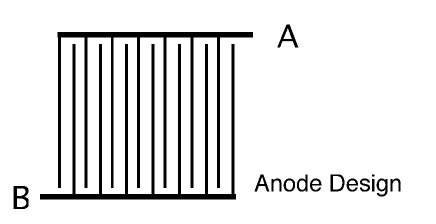
V-A Coplanar grids
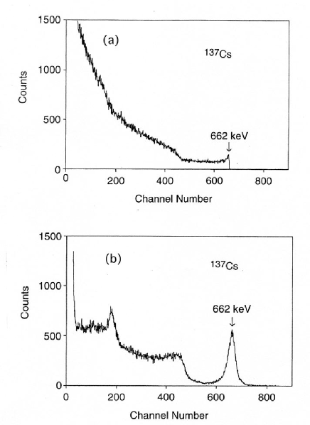
The idea of using the effects of Frisch grid found in gas and liquid detectors was proposed by Luke in 1994. In this method, an anode consisting of a pair of interleaved grids (Coplanar grid) is formed on a surface of the detector, as shown in Fig. 11 . A different bias is applied to each set of electrodes. This potential difference is small compared to the overall potential across the detector. When electrons and holes move within the bulk material of the detector, they induce equal signals on both grid electrodes. When the electrons come close to the anode plane, the signal of the grid with the higher potential rises steeply. A net signal, which is obtained by subtracting the signals from the two grids, is sensitive to primarily to the electron signal (single polarity charge sensing). Since the depth dependent signal due to the movement of holes is subtracted, the low energy tail in the spectrum can be eliminated. The dramatic improvement by the coplanar grid is demonstrated in Fig. 12 [35].
V-B Small pixels and control electrode
It has long been recognized that reducing the size of the electrode collecting the higher carriers can potentially eliminate the low-energy tail by effectively achieving single-carrier charge collection through the ”near-field effect”. Barret et al have shown that, if the pixel size is small in comparison with the detector thickness and the pixel electrode is biased to collect electrons, the incomplete charge collection due to severe hole trapping can be dramatically improved, because the induced charge on each pixel anode is dominated by the number of electrons collected by the anode[32]. For nuclear medicine applications, Barber et al. applied the idea of ”small pixel effects” to a large CdZnTe array with a pixellated electrode produced on one side of the detector slab by photolithography that is bump bonded to a readout integrated circuit which reads out each pixel individually[33]. A 6464 (2.5 cm 2.5 cm) CdZnTe arrays with 380 m pitch has been constructed and tested by Barber et al. [50]. Pixel detectors with a pixel size of several hundred to a few mm have been developed by several groups. Optimum spectroscopic performance with electrode segmentation is discussed in [36].
Recently, Butler has proposed a new concept based on a control electrode in addition to a cathode and small anode[34]. The control electrode surrounds the anode pixel and accepts a large fraction of the charges induced by the carriers while they are in transit. Similar to the effect of a coplanar grid, almost the full charge of the mobile electrons is induced on the anode. Mayer et al. extended this concept and developed an imaging device with orthogonal coplanar anodes (Fig. 13 )[37]. The signals induced on the strips are used to determine the interaction position in one dimension. The position information in the y-direction is inferred from the pixels which are interconnected to the strips. This electrode configuration provides information of pixels with 2 channels and reduces the complexity of the readout electronics. The energy resolution (FWHM) obtained from the detector is 3.42 keV at 60 keV and 5.6 keV at 662 keV.
V-C 3-D position sensitive semiconductor detector
In addition to signals from strips or pixels formed on the anode face, information from the cathode (common electrode) can be used to obtain the -ray interaction depth. The interaction depth provide a correction for the electron path length and the trapping which are important for thick detectors ( 1 cm). He et al. have performed extensive studies on this possibility[38, 39]. The fist 3-D position-sensitive semiconductor detector with CdZnTe yielded an energy resolution of 10 keV at 662 keV and a depth resolution of 0.5 mm. Results from a second generation 12.512.510 mm3 CdTe detector are reported in [40].
VI Application to Hard X-ray and -ray mission
Hard X-rays and -rays are an important frequency window for expoloring the energetic universe. The satellite has revealed us the fact that a variety of gamma-ray sources exist in the sky[41]. However, when compared with X-ray Astronomy, gamma-ray astronomy is still immature; the sensitivity of instruments are far from the level achieved by the current X-ray missions employing focusing telescopes in the energy band below 10 keV. Gamma-ray instruments in the 21st century should provide much improved angular and spectral resolution over the instruments in use today. Cadmium Telluride (CdTe) and Cadmium Zinc Telluride (CdZnTe) solid state detectors have several promising features which make them instruments for use as a focal plane imager of a multi-layer grazing incidence mirror or a coded mask aperture for the next generation of hard X-ray and -ray astronomy satellites.
VI-A INTEGRAL
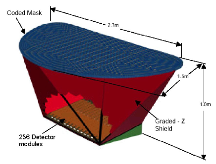
The IBIS detector on board ESA’s INTEGRAL will be the first space instrument that utilizes the good spectral resolution of CdTe. Major objectives of the mission are the detection and precise identification of -ray line spectra to study the high energy processes and resulting nuclear interactions taking place at astrophysical sites. The detector consists of two layers of pixellated detector planes separated 10 cm and operated as a focal plane detector of a coded mask aperture. The top layer detector plane is made of 16384 square CdTe detectors (442 mm3) , which gives a total sensitive area of 2621 cm2. The detector is divided into eight rectangular modules of 128 polycells, each polycell containing 16 detector pixels. In order to improve the energy resolution of the CdTe detector, a pulse height correction scheme is implemented by a specially designed ASIC. According to the measurement of a prototype detector for IBIS[42], spectral resolution of around 4.5 keV (FWHM) is obtained for the 122 keV line. The average mobilities are measured to be 94650 cm2V-1s-1 for electrons and 79.59 cm2V-1s-1 for holes while the average lifetime is reported to be 1.2 0.1 s for electrons and 4.6 0.2 s for holes.
VI-B Swift
Swift is a first of its kind multiwavelength transient observatory for -ray burst (GRB) astronomy, due to be launched in 2003. The BAT instrument on Swift is designed to provide the critical GRB trigger and quickly measure the burst position to better than 4 arcmin[43, 44]. Since the energy emission from GRBs peaks at a few 100 keV, the BAT utilizes 32768 CdZnTe detector with dimensions of 442 mm3 to form a 1.2 m 0.6 m sensitive area in the detector plane. There are 256 detector module (DM) in the BAT. One DM consists of 816 array of CdZnTe elements, which are connected to a 128 channel readout ASIC (XA chip [45]).
VI-C Future Approach
For future X-ray astronomy missions, one of the main objectives is observation with a very high sensitivity in the 10-100 keV band, where non-thermal emission becomes dominant over thermal emission[24]. This could be achieved by employing a multi-layer, grazing incidence hard X-ray telescope (“super mirror”) in conjunction with a hard X-ray imaging detector as a focal plane detector. The current goal for the imaging detector is a CdTe or CdZnTe pixel detector with both a fine position resolution of a few 100 m and a high energy resolution better than 1 keV (FWHM) in this energy range. In order to cover the field of view of the telescope, the detector should have an area of several cm2. Fast timing of several hundred ns will be required for the active shielding, which would be necessary to achieve a low background environment in space.
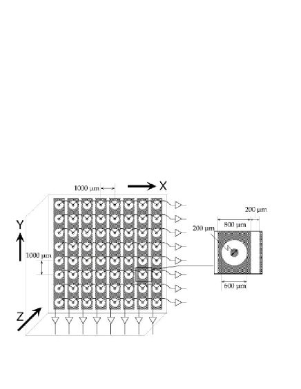
Research and development projects toward these goals are now under way by several groups[17, 46, 30, 47]. To realize fine pitch (finer than several hundred microns) CdTe and/or CdZnTe pixel detectors, good detector material and low noise amplifiers and a readout system for more than 10,000 independent channels will be the key technology. A simple and robust connection technology needs to be established, because high compression and/or high ambient temperature would damage the CdTe and CdZnTe crystal. Fig. 15 shows the radiograpic image obtained with fine pixel detectors developed under the collaboration between Bonn Universty and ISAS[48] . The size of the pixels is 200m 200 m. They are directly bump bonded to a two-dimensional photon counting ASIC (MPEC2) by using newly developed gold-stud bump bonding technology[30].
In addition to pixel detectors, a large area array ( 5000 cm2) consisting of strips has been reported in [49]. The detector is a 66 array of CdZnTe strip detectors. Orthogonal patterns are imprinted on the top and bottom sides of each detector. With strips separated by 100 m, a spatial resolution of 50 m has been demonstrated.
VII Conclusion
Owing to the significant progress in producing high quality CdZnTe and CdTe crystals, these materials are now regarded as “serious” candidates for the next generation of hard X-ray and -ray detectors. Applications to nuclear medicine are reviewd in [50, 6, 16]. Good energy resolution better than 1 keV is achieved for 60 keV -rays by the diode structure for a thin detector. A novel electrode configuration solves the problem of incomplete charge collection for the detection of high energy -rays with a thick detector. As discussed by Fougeres et al. [19], the choice between CdTe and CdZnTe is still very difficult to make. There is still some room for improvements for real applications. These include the production of large and uniform single crystals, especially for the HPB-grown CdZnTe, and the bump technology specific to “fragile” CdTe and CdZnTe. The cost of the material is still high for a large scale -camera. Further advances in application-specific integrated circuits (ASICs) are necessary for the fabrication of fine-pitch pixel detectors. Extensive studies currently underway by many laboratories will boost the further advances of of these interesting materials .
VIII Acknowledgment
We acknowledge constructive discussion with R. Ohno and C. Szeles. We thank G. Sato, M. Kouda, Y. Okada for the help of experiments and M.D. Audley for his critical reading of the manuscript.
References
- [1] M. Richter and P. Siffert, “High resolution gamma ray spectroscopy,” Nucl. Instr. Meth., vol. A322, pp. 529-537, 1992.
- [2] P. Siffert, “Cadmium telluride and related materials as X- and gamma-ray detectors: A review of recent progress,” Proc. SPIE, vol. 2305, pp. 98-109, 1994.
- [3] Y. Eisen, “Current state-of-the-art industrial and research applications using room-temperature CdTe and CdZnTe solid state detectors,” Nucl. Instr. Meth., vol. A117, pp. 431-439, 1974.
- [4] F.L. Augustine, “High resolution gamma ray spectroscopy,” Nucl. Instr. Meth., vol. A353, pp. 201, 1994.
- [5] P. Weilhammer, A. Nygrad, W. Dulinski, A. Czermak, F. Djama, S. Gadomski, S. Roe, A. Rudge, F. Schopper, J. Strobel, “Si pad detectors,” Nucl. Instr. Meth., vol. A383, pp. 89-97, 1996.
- [6] C. Scheiber, “CdTe and CdZnTe gamma ray detectors in nuclear medicine,” Nucl. Instr. Meth., vol. A448, pp. 513-524, 2000.
- [7] J.S. Iwanczyk, B.E. Patt, Y.J. Wang, A. Kh. Khusainov, “Comparison of HgI2, CdTe, and Si (p-i-n) X-ray detectors,” Nucl. Instr. Meth., vol. A380, pp. 186-192, 1996.
- [8] W. Bencivelli, E. Bertoulucci, U. Bottigli, A. Del Guerra, A. Messineo, W.R. Nelson, P. Randaccio, et al., “Evaluation of elemental and compound semiconductors for X-ray digital radiography,” Nucl. Instr. Meth., vol. A310, pp. 210-214, 1991.
- [9] Geant4, available from http:wwwinfo.cern.ch/asd/geant4/geant4.html
- [10] F.P. Doty, J.F. Butler, J.F. Schetzina, and K.A. Bowers, “Properties of CdZnTe crystals grown by a high pressure Bridgman method,” J Vac. Sci. Technol., vol. B10, pp. 1418-1422, 1992.
- [11] J.F. Butler, C.L. Lingren and F.P. Doty “Cd1-xZnxTe Gamma-ray Detectors,” IEEE Trans. Nucl. Sci., vol. 39, 4, pp. 605-609, 1992.
- [12] C. Szeles, M.C. Driver, “Growth and properties of semi-insulating CdZnTe for radiation detector applications,” Proc. SPIE, vol. 3446, pp. 1-8, 1998.
- [13] J.E. Toney, T.E. Schlesinger, and R.B.James, “Optimal bandgap variants of Cd1-xZnxTe for high-resolution X-ray and gamma-ray spectroscopy,” Nucl. Instr. Meth., vol. A428, pp. 14-24, 1999.
- [14] C. Szeles, E.E. Eissler, D.J. Reese, S.E. Cameron, “Radiation Detector Performance of CdTe Single Crystals Grown by the Conventional Vertical Bridgman Technique,’ Proc. SPIE, vol. 3768, pp. 98-107, 1999.
- [15] A. Burger, K. Chattopadhyay, H. Chen, X. Ma, J-O. Ndap, M. Scheiber, et al., “Defects in CZT crystals and their relationship to gamma-ray detector performance,” Nucl. Instr. Meth., vol. A448, pp. 586-590, 2000.
- [16] Y. Eisen, A. Shor, I Mardor, “CdTe and CdZnTe gamma ray detectors for medical and industrial imaging system,” Nucl. Instr. Meth., vol. A428, pp. 158-170, 1999.
- [17] C.M. Stahle, B.H. Parker, A.M. Parsons, L.M. Barbier, S.D. Barthelmy, N.A. Gehrels, D.M. Palmer, S.J. Snodgrass and J. Tuller, “CdZnTe and CdTe detector array for hard X-ray and gamma-ray astronomy,” Nucl. Instr. Meth., vol. A436, pp. 138-145, 1999.
- [18] M. Funaki, T. Ozaki, K. Satoh, and R. Ohno, “Growth and Characterization of CdTe Single Crystal for Radiation Detectors,” Nucl. Instr. Meth., vol. A436, pp. 120-126, 1999.
- [19] P. Fougeres, P. Siffert, M. Hageali, J.M. Koebel, R. Regal, “CdTe and Cd1-xZnxTe for nuclear detector: facts and fictions,” Nucl. Instr. Meth., vol. A428, pp. 38-44, 1999.
- [20] K. Hecht,”Zum Mechanismus des lichtelektrischen Primärstromes in isolierenden Kristallen,” Zeits, Phys., vol. 77, p. 235, 1932.
- [21] Chr. Bargoltz, E. Fumero, and L. Martensson, “Model-based pulse shape correction for CdTe detectors,” Nucl. Instr. Meth., vol. A434, pp. 399-411, 1999.
- [22] R. Arlt and D.E. Rundquist, “Room temperature semiconductor detectors for safeguards measurements,” Nucl. Instr. Meth., vol. A380, pp. 455-461, 1996.
- [23] G.F. Knoll, Radiation Detection and Measurement. 3rd ed., John Wiley & Sons Inc., New York, 2000.
- [24] T. Takahashi, B. Paul, K. Hirose, C. Matsumoto, R. Ohno, T.Ozaki, K. Mori, and Y. Tomita “High-resolution Schottky CdTe diode for hard X-ray and gamma-ray astronomy,” Nucl. Instr. Meth., vol. A436, pp. 111-119, 1999.
- [25] R. Arlt, V. Ivanov, and A. Khusainov, “Advances in High-Resolution CdTe and Large Volume CdZnTe Detectors,” Proc. SPIE, vol. 3115, pp. 76-89, 1994.
- [26] M. Niraula, D. Mochizuki, T. Aoki, Y. Hatanaka, Y. Tomita, T. Nihashi, “Improved spectrometric performance of CdTe radiation detectors in a p-i-n design,” Appl. Phys. Lett., vol. 75, 15, pp. 2322-2324, 1999.
- [27] T. Takahashi, K. Hirose, C. Matsumoto, K. Takizawa, R. Ohno, T. Ozaki, K. Mori, and Y. Tomita “Performance of a New Schottky CdTe Detector for Hard X-ray Spectroscopy,” Proc. SPIE, vol. 3446, pp. 29-37, 1998.
- [28] C. Matsumoto, T. Takahashi, K. Takizawa, R. Ohno, T. Ozaki, and K. Mori “Performance of a New Schottky CdTe Detector for Hard X-ray Spectroscopy,” IEEE Trans. Nucl. Sci., vol. 45, pp. 428-432, 1998.
- [29] T. Ozaki, Y. Iwase, H. Takamura, and M. Ohmori, “Thermal treatment of CdTe surfaces for radiation detectors,” Nucl. Instr. Meth., vol. A380, pp. 141-144, 1996.
- [30] T. Takahashi, S. Watanabe, M. Kouda, G. Sato, S. Kubo, Y. Kuroda et al., “High Resolution CdTe Detector and Applications to Imaging Devices,” IEEE Trans. Nucl. Sci. 2001 in press.
- [31] P.N. Luke, “Single-polarity charge sensing in ionization detectors using coplanar electrodes,” Appl. Phys. Lett. vol. 65 pp. 2884-2886, 1994.
- [32] H.H. Barrett, J.D. Eskin, H.B. Barber, “Charge Transport in Arrays of Semiconductor Gamma-Ray Detector,” Phys. Rev. Lett., vol. 75, pp. 156-159, 1995.
- [33] H.B. Barber, D.G. Marks, B.A. Apotovsky, F.L.Augustine, H.H. Barret, J.F. Butler, E.L. Dereniak, et al., “Progress in developing focal-plane-multiplexer readout for large CdZnTe arrays for nuclear medicine applications,” Nucl. Instr. Meth., vol. A380, pp. 262-265, 1996.
- [34] J.F. Butler, “Novel electrode design for single-carrier charge collection in semiconductor nuclear detectors,” Nucl. Instr. Meth., vol. A396, pp. 427-430, 1997.
- [35] P.N. Luke, “Electrode configuration and energy resolution in gamma-ray detector,” Nucl. Instr. Meth., vol. A380, pp. 232-237, 1996.
- [36] A. Shor, Y. Eisen, and I. Mardor, “Optimum spectroscopic performance from CZT - and X-ray detectors with pad and strip segmentation,” Nucl. Instr. Meth., vol. A428, pp. 182-192, 1999.
- [37] M.L. McConnel, J.R. Macri, J.M. Ryan, K. Larson, L.-A. Hamel, G. Bernard et al., “Three-dimensional imaging and detection efficiency performance of orthogonal coplanar CZT strip detectors,” Proc. SPIE, vol. 4141, pp. 157-167, 2000.
- [38] Z. He, “1-D position sensitive single carrier semiconductor detectors,” Nucl. Instr. Meth., vol. A380, pp. 228-231, 1996.
- [39] Z. He, W.Li, G.F. Knoll, D.K. Wehe, J. Berry, C.M. Stahle, “3-D position sensitive CdZnTe gamma-ray spectrometers,” Nucl. Instr. Meth., vol. A422, pp. 173-178, 1999.
- [40] W. Li, Z. He, G.F. Knoll, and D.K. Wehe, “Interaction Depth in CdTe/CdZnTe Spectrometers by Electron Drift Time,” submitted to IEEE Trans. Nucl. Sci. 2001.
- [41] N. Gehrels and J. Paul, “The new gamma-ray astronomy,” Physics Today, vol. 51, no 2, pp. 26-32, 1998.
- [42] O. Limousing, C. Blondel, J. Cretolle, H. Dzitko, P. Laurent, F. Lebrun, J.P. Leray, et al. “The ISGRI CdTe gamma-ray camera first steps,” Nucl. Instr. Meth., vol. A442, pp. 244-249, 2000.
- [43] N. Gehrels, “The Swift Gamma Ray Burst MIDEX,” SPIE, vol. 4140, pp. 42-49, 2000.
- [44] S. D. Barthelmy, “The Burst Alert Telescope (BAT) on the Swift MIDEX mission,” SPIE, vol. 4140, pp. 50-63, 2000.
- [45] Integrated Detector and Electronics AS, Norway, http://www.ideas.no
- [46] J.L. Matteson, F. Duttweiler, G.L. Huszar, P.C. Leblanc, R.E. Skelton, E.A. Stephan et al., “Position-sensitive CZT detector module,” SPIE, vol. 3446, pp. 192-201 1998.
- [47] V.V.Sushkov, W.J.Hamilton, K.Hurley, D.G.Maeding, H. Ogelman, R.J. Paulos, et al. “Preliminary Test Results of a New High Energy Resolution Silicon & CdZnTe Pixel Detectors for Application to X-ray Astronomy,” SPIE, vol. 3765, pp. 379-387 1999.
- [48] P. Fischer, M. Kouda, H. Krueger, M. Lindnera, G. Sato, T. Takahashi, S. Watanabe, and N. Wermes, “A Counting CdTe Pixel Detector for Hard X-ray Imaging,” submitted to IEEE Trans. Nucl. Sci. 2001.
- [49] C.M. Stahle, Z.Q. Shi, K.Hu, S.D. Barthlmy, S.J. Sodgrass, L.M. Barlett et al., “Fabrication of CdZnTe strip detectors for large area arrays,” Proc. SPIE, vol. 3115, pp. 90-97, 1997.
- [50] H.B. Barber, “Applications of semiconductor detectors to nuclear medicine,” Nucl. Instr. Meth., vol. A436, pp. 102-111, 1999.