Diffraction-limited operation of micro-metalenses: fundamental bounds and designed rules for pixel integration
Abstract
Metasurfaces provide a compact, flexible, and reliable solution for controlling the wavefront of light. In imaging systems, micro-lens arrays are integrated with pixel matrices to reduce optical crosstalk, enhance photon collection efficiency, and improve spatial resolution. However, as the aperture size of the photonic devices decreases, fundamental limitations associated with diffraction emerge. Here, we theoretically analyze and experimentally demonstrate that these constraints also affect the performance of small functionalized apertures, including metasurfaces and metalenses, emphasizing the increasing impact of diffraction at small pixel sizes. Despite their design versatility, our findings reveal the necessity of accounting for fundamental diffraction properties to optimize the performance of miniature optical metasurfaces.
1]\orgdivUniversité Côte d’Azur, \orgnameCNRS, CRHEA, \orgaddress\streetRue Bernard Gregory, \cityValbonne, \postcode06560, \countryFrance 2]\orgdivIII-V Lab, \orgaddress\street1 Avenue Augustin Fresnel, \cityPalaiseau, \postcode91767, \countryFrance 3]\orgdivPhysics department, \orgnameColorado School of Mines, \orgaddress\street1523 Illinois Street, \cityGolden, CO, \postcode80401, \countryUSA
1 Introduction
Metasurfaces (MSs) consist of an arrangement of subwavelength nanostructures whose geometries and materials are carefully engineered to produce a specific response in phase and/or polarization [1, 2, 3]. Their operating principle relies on the collective optical response of an ensemble of nanostructures to produce user-defined optical functions. As this disruptive optical technology advances toward industrial applications, a new set of challenges associated with its integration into specific applications is emerging [4]. Despite the enormous amount of recent research on MSs, studies aimed at identifying their physical limits remain elusive. Intriguingly, we observed that small MSs are not operating as expected when their diameters reach the order of a few wavelengths or less [5, 6]. This behavior, which might at first appear as unexpected, is of particular interest in the context of vertical integration of MS in imaging systems to improve the performance of optical sensors. The vertical integration of MSs with semiconductor technologies, successfully implemented in the context of controlled laser emission [7, 8, 9, 10, 11], might also bring additional industrial prospects in light field imaging [12, 13] and LiDAR [14, 15, 16], assuming that MSs are properly designed.
Image sensor technology has benefited from the reduction in pixel size to improve both spatial resolution with higher pixel density and signal-to-noise ratio by reducing dark current [17]. Currently, pixel sizes are reaching a critical limit of only a few wavelengths, but further reduction in pixel size introduces two major drawbacks, electrical and optical crosstalk, that hinder the modulation transfer function of the imaging system. These issues are conventionally circumvented by integrating an injection-molded array of microlenses directly onto the sensor matrix [18, 19]. However, these solutions are bulky and incur relatively expensive assembly and packaging costs to the imaging system. Additionally, molded lenses designed to be roughly the size of the pixel are characterized by an asymmetric focusing shape with a maximum intensity occurring before the designed focal length, an effect known as the focal shift [20]. Recent efforts to improve the optical function of conventional microlens arrays using MS are currently being investigated, as this approach could drastically simplify the fabrication process and offer new imaging functionalities, including spectral and polarization selectivity. However, the integration of these small functionalized optical apertures on top of small pixels also comes with fundamental limitations.
Here, we propose identifying these fundamental limits, focusing particularly on the design of small metalenses, to clarify the different regimes of operation. We use a theoretical model previously proposed for small diffracting apertures, which is based on vectorial diffraction theory [21], to account for planar apertures with spatially varying optical responses. We show that the domain of validity is bounded between (i) a hard limit defined by the MS size and (ii) a soft limit defined by the MS nanostructuration, i.e., the periodicity of the metasurface building blocks. First, we introduce the notion of focal shift and, in the following section, we present the formalism indicating the strong expected impact of the focal shifts for sufficiently small devices. Finally, we present the experimental results obtained using GaN metalens of various numerical apertures (NA), which validate our theoretical predictions.
2 Results
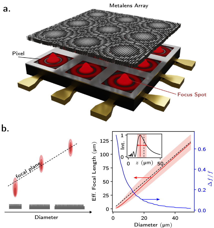
Fig. 1(a) illustrates the concept of vertical integration of a metalens array onto a sensor. All metalenses depicted in the schematic are identical and designed to focus light along their optical axis, i.e. at the center of their respective pixels. We begin our investigation by numerically calculating, using diffraction theory, the focal distance of a metalens as a function of its diameter with a fixed numerical aperture (NA) given by,
| (1) |
where is the radius of the lens, its focal distance, and the refractive index of the medium. Here, we consider that only a layer of air () separates the metalens array from the absorbing pixels. From this expression, we see that decreasing the radius of a metalens with fixed NA should result in a proportional decrease in its focal length. However, in practice, when the lens reaches a critical aperture size, this simple law breaks down, as illustrated in the numerical calculations presented in Fig. 1(b). Instead, we observe that for a diameter smaller than and a wavelength of , the maximum intensity, or effective focal length, occurs at a shorter distance than the designed focal length. At the same time, the spot becomes highly asymmetric along the propagation direction, with the maximum intensity shifted closer toward the metalens. This phenomenon has been previously reported as the so-called focal shift [20]. The origin of the focal shift is related to the diffraction that occurs when the size of the metalens aperture approaches the operation wavelength .
2.1 General Theory of Diffraction By Wavelength-scale Apertures
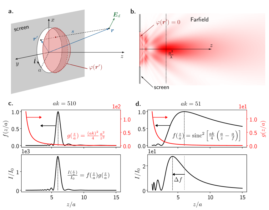
We consider the transmission of a plane wave from the -negative region of space through a metasurface of aperture , with radius , and located in the plane (see Fig. 2(a)). We assume that the electromagnetic fields at are zero everywhere outside of the aperture, and that inside the aperture, it is noted . The presence of field discontinuities in the aperture plane results in wide-angle beam deflection, which can be rigorously treated mathematically using a vectorial formulation of the diffraction problem. Its solution is given by the Stratton-Chu integral [21, 22]. Adopting the Gaussian unit system, the diffracted electric field distribution after the aperture reads as
| (2) | ||||
with the Green’s function. The unit vector points towards the negative space, i.e. , and the unit vector , tangent to the aperture, is defined in the positive direction with regards to the normal . The surface integral on the right-hand side of Eq. (2) describes the field radiated by sources of electric and magnetic currents, as well as charge distribution, inside the aperture. Under certain assumptions, this term alone can be reduced to the well-known expressions of Fresnel and Fraunhöfer diffraction theory [23]. However, the field described only by the surface integral does not properly satisfy Maxwell’s equations at the location of the aperture. To derive Eq. (2), we assume that the fields and their derivatives should be continuous on the screen and aperture. This is not the case as and while increasing the radius to pass the contour delimiting the aperture. The contour integral in Eq. (2) resolves this inconsistency by considering Maxwell’s continuity equations of the fields on the screen through the contour of the aperture [24].
In order to compute the diffracted field by the metasurface, we need to determine the electromagnetic field , inside the aperture. For a metasurface, with a spatially varying phase profile and transmission coefficient , the wavefront of the transmitted light thus follows the generalized law of refraction [1, 25],
| (3) |
with and the transverse wavevector of the incident wave and of the transmitted wave, respectively and a vector composed of the derivatives of the phase profile. Consequently, the transmitted wave is not necessarily a plane wave; in the case of metalenses the wavefront is spherical. Moreover, according to Maxwell’s equations, the electric field is locally transverse to the direction of propagation, therefore the curvature of the wavefront leads to a complex distribution of polarization of the transmitted wave. In the particular case of spherical metalenses, we can determine this polarization pattern and thus express the electromagnetic field inside the aperture, cf. supplementary note LABEL:sm-sec:vectorial_diff.
2.2 Origin of the Focal Shift
To describe the focal shift, it is sufficient to look at the diffracted electric field on the optical axis . By symmetry, for a metalens, only the component of the electric field parallel to the incident polarization remains, since the orthogonal components cancel on the optical axis, cf. supplementary note LABEL:sm-sec:vectorial_diff. Therefore, Eq. (2) can be treated analytically. In the following, we assume that the metasurface has unitary and uniform transmission, .
We first consider the case of a plain aperture, represented in Fig. 2(b) with homogeneous response. We are interested in the field at a large distance from the aperture. In this case, the intensity along the -axis at , derived in supplementary note LABEL:sm-sec:ap_circAperture, is given by
| (4) |
A map of the intensity distribution in the -plane, obtained after solving Eq. (2), is plotted in Fig. 2(b). Equation (4) illustrates a known result: even in the absence of a phase profile, a circular aperture, i.e. a pinhole, focuses light at a certain distance . A detailed study of the intensity function , in supplementary note LABEL:sm-sec:ap_circAperture, shows that the maximum of intensity is approximately obtained for
| (5) |
The asymmetry in the shape of the focal spot arises from the dependence of the argument of on the inverse distance .
Now, we consider the case of a metasurface placed in the aperture and with an hyperbolic phase profile given by the equation,
| (6) |
Since, we are interested in the region of focal shift, and therefore, we can simplify Eq. (2). Similarly to the case of the plain aperture in Eq. (4), we derive, in the supplementary note LABEL:sm-sec:circLens, the intensity distribution along the optical axis for , for a metalens with numerical aperture lower than ,
| (7) |
Equation (7) is analogous to Eq. (4) except for an additional term in the related to the focal distance of the metalens. The effective focal length is given by the location of the maximum intensity, which results from the product of the two terms: (i) the function representing the z-focusing profile and (ii) the intensity decay, which is proportional to . When considering metalenses with a large focal length compared to their aperture size , , the intensity distribution converges to that of the homogeneous aperture. This is not entirely surprising as implies that the profile at the aperture plane is converging to a constant spatial phase value. Conversely, if the focal distance is smaller than the aperture of the metalens, , the metalens will focus when the is maximal, at . In the intermediate regime, however, the maximum of intensity is not obtained at even though the is maximal. Indeed, the intensity is quenched by the term . The effective focal distance will depend on the relative value between the aperture size , the focal distance , and the operating wavelength . For example, fixing the focal distance , on one hand, for a large quantity , i.e. for a large aperture compared to the wavelength, the width of the is thin and thus the effect of intensity decrease will be negligible, cf. Fig. 2(c). On the other hand, for smaller , the term is large and asymmetric, leading to a strong focal shift at a shorter distance than the expected focal length, cf. Fig. 2(d).
The interplay between the three fundamental properties of a lens, i.e. the characteristic size of the lens, the focal length, and the operating wavelength, is summarized in the Fresnel number [26],
| (8) |
An expression of Eq. (7) in terms of the Fresnel number is given in the supplementary note LABEL:sm-sec:circLens. In the literature, the Fresnel number is often referred to as the number of half-wavelengths in the wavefront at the edge of the aperture [27]. This derivation can also be obtained for a small numerical aperture by performing a Taylor expansion of expression Eq. (6). Our analysis in supplementary note LABEL:sm-sec:ap_circAperture also suggests that the Fresnel number can be interpreted as the ratio of the focal distance of the plain aperture to the characteristic length of the optical function achieved inside the aperture ,
| (9) |
For , the optical function is achieved before the focal spot of the aperture, meaning that the metalens primarily acts as a lens. Conversely, for the optical function is achieved beyond the focal spot of the aperture, so the metalens primarily acts as a simple aperture. In other words, the aperture selects only a small part of the overall focused phase information, i.e., reducing the overall phase curvature to what is in the aperture. We define the diffraction-limited operation regime of micro-metalenses, the regime where the diffraction of the aperture itself compromises the metasurface’s optical function.
To visually illustrate the evolution of the Fresnel number as a function of the three fundamental parameters, we plotted in Fig. 3(a) a mapping of the Fresnel number as a function of the number of wavelengths inside the aperture and also indicating the numerical aperture. In the case of microlenses, for example , the Fresnel number is less than for numerical apertures smaller than approximately , suggesting a strong focal shift. To avoid focal shift, then, metalenses would require a larger NA. Additionally, we can also identify a minimal numerical aperture, , for which we would have and thus, the micro-metalenses would not behave significantly differently from an aperture. From Fig. 3(a), we can also see that the focal shift occurs mainly with small metalenses. For , the Fresnel number exceeds for nearly any numerical aperture above .
2.3 Limitation of the phase sampling
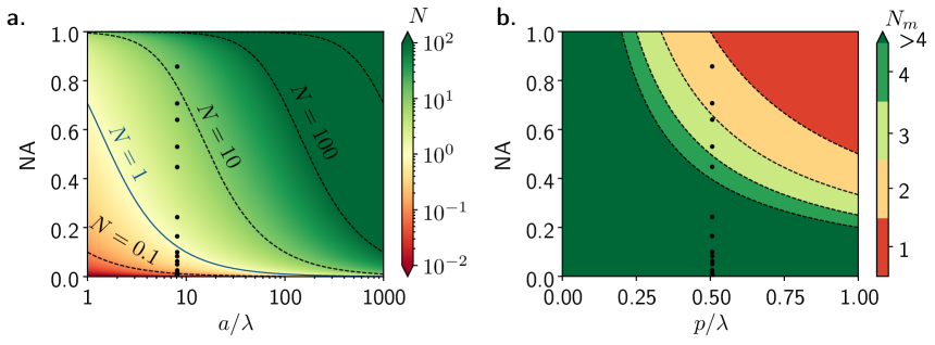
So far, the phase profiles imparted by the metasurface have been considered continuous. In practice, phase shifts are induced by discrete meta-atoms of finite size. For adequate sampling of the phase profile, we require at least meta-atoms per Fresnel zone. Following this rule, we obtain, in supplementary note LABEL:sm-sec:sampling, a second limit for metalenses,
| (10) |
with the period separating two adjacent metasurface building blocks. This is a soft limit, and achieving higher discretizations depends on the capacity of our technological platform to fabricate sufficiently small meta-atoms to meet the condition (10). According to the Shannon-Nyquist sampling theorem, to properly sample the phase profile, only two meta-atoms per Fresnel zone are sufficient. However, for such sampling, the Strehl ratio of a metalens was estimated to reach only a value of [28]. Achieving Strehl ratios associated with diffraction-limited performance, beyond , requires at least four elements per Fresnel zone, . For phase profile (6) with fixed focal length, the size of a Fresnel zone decreases and converges toward as we move further away from the device center. This results from the linear asymptotic behavior of the phase profile at large distance , bending the light at . This limit is obtained only for large distances from the metalens center, that is, for diameters that easily exceed the metalens aperture size. For micro-metalenses, which are designed with extremely small diameters, barely equal to a few wavelengths, this distance is quickly reached, resulting in poor sampling of the phase profile.
Similarly to the previous section, we can visually represent Eq. (10) by plotting the number of elements per Fresnel zone in Fig. 3(b). The plot shows that, to achieve optimal performance for optical micro-metalenses, one should avoid the diffractive regime by increasing the numerical aperture, but it also requires designing structures with smaller critical dimensions.
2.4 Fabrication and Experimental Characterization
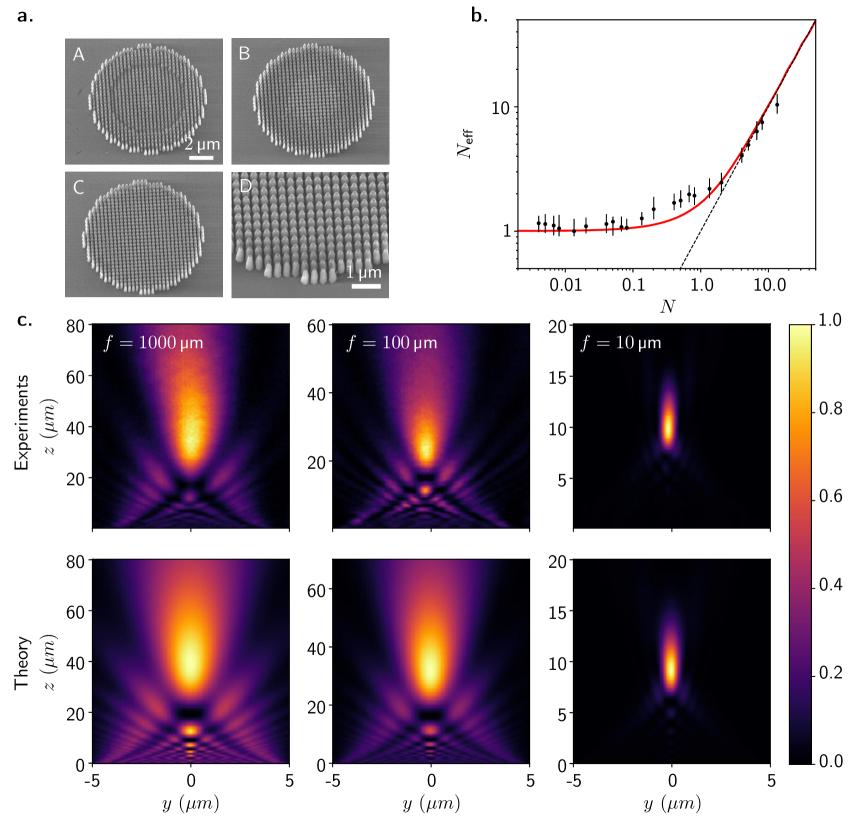
To validate our approach, we experimentally characterized an array of -wide metalenses, see Fig. 4(a) and method 4.1. The fabricated meta-atoms are arranged on a square grid with period designed to operate at wavelength . Therefore, in Fig. 4(a) we are located at and in Fig. 3(b) at . We realized an array of metalenses with fix diameters of and with varying focal length ranging from to . Metalenses with focal length smaller than would have a numerical aperture higher than the numerical aperture of our objective (). Each metalens was characterized by a -scan setup to determine its effective focal length.
The experimental z-scan intensity mappings are presented in Fig. 4(c) for designed focal length of , and and compared with numerical simulation where we solved Eq. (2). The z-scan characterization setup is described in method 4.2. Our results show acceptable agreement. The effective Fresnel number of the fabricated metalenses is plotted in Fig. 4(b). The error bars represent the accumulated uncertainty in determining the metasurface plane for each metalens, as well as the maximum intensity, which is evaluated around 80% of the maximum intensity. For low Fresnel numbers, , the metalenses behave as simple apertures with effective Fresnel numbers approaching . For Fresnel numbers comprised between and , slight deviations of experimental measurements from theoretical results are attributed to our fabrication processes, which lead to imperfect optical performance. For Fresnel numbers comprised between and , experimental results agree with the theory, following the expected linear dependency Eq. (1).
3 Discussion
Replacing refractive microlenses with vertically integrated metalenses arrays offers an innovative technological alternative to improve spatial resolution and reduce the integration issues. While there are fundamental optical and fabrication consideration, these challenges present opportunities for creative integration and design solutions. Designing such a compact metalens array involves finding an optimal compromise between the metalens numerical aperture and its structural parameters.
For a fixed Fresnel number, Eq. (8) predicts that decreasing the metalens diameter by a factor results in a focal length reduction by . In most large metalenses, meaning their diameter greatly exceeds the operating wavelength, accuracy in the focal point is not an issue. However, designing small microlenses, such as those with dimensions below used in camera pixels to enhance detectivity, requires carefully selecting the right NA and design assembly. We demonstrated that in low-NA microlenses associated with low Fresnel numbers, diffraction effects dominate, limiting the lens performance. With high-NA microlenses, the period of the meta-atoms forming the metasurface should satisfy the condition in Eq. (10), otherwise, the sampling period will be insufficient to ensure optimal diffraction-limited performances. Additionally, metalens array integration generally requires dealing with the chip substrate, which incidentally could modify the effective wavelength and the Fresnel number, requiring further adjustments in design, including sampling period and focal distance.
We identified four distinct operational regimes: (i) the diffraction regime, where diffraction dominates and the metalens function as a simple aperture; (ii) the hybrid-diffractive regime, where the lensing effect is present but strongly affected by the diffraction; (iii) the metasurface regime, where the metalens operates effectively with proper wavefront control; and (iv) the metasurface sampling-limited regime, where high NA wavefront engineering requires improving the technical processes to address higher aspect ratio fabrication.
Maximizing light collection on a conventional 2D square pixel array is more effective with square lenses rather than circular lenses discussed here. Since the NA is defined for optical lenses with revolution symmetry, the Fresnel number of a square metalens, , falls within the range , which provides a useful information for design consideration, according to the operation regimes outlined above.
Following this discussion, a natural question emerges: when is it better to use a metasurface than a conventional aperture? To answer this question, we can look at the focusing efficiency, defined by the amount of power going through one pixel, divided by the amount of power transmitted through the metasurface, see supplementary note LABEL:sm-sec:focal_efficiency. For Fresnel number larger than , metasurfaces act better than an actual aperture. However, with a non-optimized approach, such as a using a fixed library of elements on fix grid, gain in terms of focusing efficiency could be only few percent. Since, for micro-metalenses, the number of different meta-atoms is only about few dozens, we believe optimization methods [29] could be particularly interesting for such applications.
In conclusion, we explore the fundamental limitations of miniaturized metalenses, with sizes only a few times the operation wavelength. Using diffraction theory, we modeled a finite-sized ideal metasurface and analyzed how the metalens’ dimensions impact its optical functionality. Our findings reveal two key operational regimes based on the device’s Fresnel number. Operating metalenses in the diffractive regime (low Fresnel number) presents challenges due to the alteration of the wavefront by the diffraction resulting from the metasurface aperture, making the aperture optical functionalization ineffective. Instead, for arrays made of very small metalenses, when working at visible/IR wavelengths, achieving a high numerical aperture and thus a short focal length is essential for optimal focusing properties. This work provides new insights into metalens integrations and discusses the design opportunities available for compact imaging systems, particularly when the photonic devices are directly fabricated onto the pixel matrices. Our results indicate that, depending on parameters, metasurfaces could be a versatile platform for enhancing imaging capabilities, paving the way for next-generation sensor technology.
4 Methods
4.1 Metalenses Fabrication
The metalenses have been fabricated by employing -thick GaN epitaxially grown by metal organic vapor phase epitaxy on a double side polish sapphire substrate. The metalenses were patterned by exposing a double layer of PMMA resist using a focused electron beam, followed by development, and deposition of a Ni mask of . The cylindrical -thick GaN nanopillars have finally been etched on the substrate by employing an inductively coupled plasma reactive ion etching process based on and followed by the chemical removal of the metallic mask in the Piranha solution.
4.2 Z-scan Characterization
A collimated LED light source was used to illuminate the metalenses. The sample holder was mounted on a motorized translation stage controlled by a closed-loop picomotor controller. The size of the translation stage step is . An objective, with magnification and numerical aperture, is used to image each metalens separately onto a camera. The plane of the metalens was visually determined by the camera. Due to the uncertainty in determining this plane, we identified the translation range for which we could consider the image on camera to be in the plane of the metasurface and estimated this uncertainty to be within the range .
Data Availability Data that support the plots in this paper and other findings of this study are available from the corresponding authors upon reasonable request.
Code Availability The codes for numerical simulations of this study are available from the corresponding authors upon reasonable request.
Acknowledgements PG, NK, JLR, SK acknowledge financial support from the French National Research Agency ANR Project Millesime 2 (ANR-21-ASTR-0014). SK acknowledges financial support from the European Defense fund EDF project Mini-Bot (EDF-2021-OPEN-R-SME-2). RC was supported by the French government through the France 2030 investment plan managed by the National Research Agency (ANR), as part of the Initiative of Excellence Université Côte d’Azur under reference number ANR-15-IDEX-01. PG and CK acknowledge financial support from the French National Research Agency ANR Project SWEET (ANR-22-CE24-00005).
Author Contributions PG and JLR conceived this study. NK worked on the theoretical part, the numerical simulations and optical characterization. PMC grew the GaN template used for the fabrication of the metalenses. CK did the fabrication processes. VB helped with the electron-beam lithography as well as for SEM characterization. RC, JLR, SK and PG reviewed and edited the manuscript. All authors edited the manuscript at several stages and contributed to the references.
Competing Interests The authors declare no competing interests.
References
- \bibcommenthead
- [1] Yu, N. et al. Light Propagation with Phase Discontinuities: Generalized Laws of Reflection and Refraction. Science 334, 333–337 (2011).
- [2] Genevet, P., Capasso, F., Aieta, F., Khorasaninejad, M. & Devlin, R. Recent advances in planar optics: From plasmonic to dielectric metasurfaces. Optica 4, 139–152 (2017).
- [3] Yu, N. & Capasso, F. Flat optics with designer metasurfaces. Nature Materials 13, 139–150 (2014).
- [4] Yoon, G., Tanaka, T., Zentgraf, T. & Rho, J. Recent progress on metasurfaces: Applications and fabrication. Journal of Physics D: Applied Physics 54, 383002 (2021).
- [5] Jia, Y. Focal shift in metasurface based lenses. Optics Express 26, 8001–8015 (2018).
- [6] Gao, Y. et al. Analysis of focal-shift effect in planar metallic nanoslit lenses. Optics Express 20, 1320–1329 (2012).
- [7] Xie, Y.-Y. et al. Metasurface-integrated vertical cavity surface-emitting lasers for programmable directional lasing emissions. Nature Nanotechnology 15, 125–130 (2020).
- [8] Ni, P.-N. et al. Spin-decoupling of vertical cavity surface-emitting lasers with complete phase modulation using on-chip integrated Jones matrix metasurfaces. Nature Communications 13, 7795 (2022).
- [9] Wen, D., Meng, J., Cadusch, J. J. & Crozier, K. B. VCSELs with On-Facet Metasurfaces for Polarization State Generation and Detection. Advanced Optical Materials 9, 2001780 (2021).
- [10] Wang, Q.-H. et al. On-Chip Generation of Structured Light Based on Metasurface Optoelectronic Integration. Laser & Photonics Reviews 15, 2000385 (2021).
- [11] Zheng, C.-L., Ni, P.-N., Xie, Y.-Y. & Genevet, P. On-chip light control of semiconductor optoelectronic devices using integrated metasurfaces. Opto-Electronic Advances 8, 240159–26 (2025).
- [12] Lin, R. J. et al. Achromatic metalens array for full-colour light-field imaging. Nature Nanotechnology 14, 227–231 (2019).
- [13] Fan, Q. et al. Trilobite-inspired neural nanophotonic light-field camera with extreme depth-of-field. Nature Communications 13, 2130 (2022).
- [14] Wang, X. et al. Advances in information processing and biological imaging using flat optics. Nature Reviews Electrical Engineering 1, 391–411 (2024).
- [15] Juliano Martins, R. et al. Metasurface-enhanced light detection and ranging technology. Nature Communications 13, 5724 (2022).
- [16] Majorel, C. et al. Bio-inspired flat optics for directional 3D light detection and ranging. npj Nanophotonics 1, 1–10 (2024).
- [17] Rogalski, A., Martyniuk, P. & Kopytko, M. Challenges of small-pixel infrared detectors: A review. Reports on Progress in Physics 79, 046501 (2016).
- [18] Cai, S. et al. Microlenses arrays: Fabrication, materials, and applications. Microscopy Research and Technique 84, 2784–2806 (2021).
- [19] Béguelin, J., Voelkel, R. & Scharf, T. Commented review on refractive microlenses and microlens arrays metrology. Journal of Optical Microsystems 1, 030901 (2021).
- [20] Li, Y. & Wolf, E. Focal shifts in diffracted converging spherical waves. Optics Communications 39, 211–215 (1981).
- [21] Bouwkamp, C. J. Diffraction Theory. Reports on Progress in Physics 17, 35–100 (1954).
- [22] Stratton, J. A. & Chu, L. J. Diffraction Theory of Electromagnetic Waves. Physical Review 56, 99–107 (1939).
- [23] Born, M. & Wolf, E. Principle of Optics 7th edn (Cambridge, 1999).
- [24] Kottler, F. Elektromagnetische Theorie der Beugung an schwarzen Schirmen. Annalen der Physik 376, 457–508 (1923).
- [25] Aieta, F. et al. Out-of-Plane Reflection and Refraction of Light by Anisotropic Optical Antenna Metasurfaces with Phase Discontinuities. Nano Letters 12, 1702–1706 (2012).
- [26] Li, Y. Dependence of the focal shift on Fresnel number and f number. JOSA 72, 770–774 (1982).
- [27] Wang, W. & Wolf, E. Far-zone behavior of focused fields in systems with different Fresnel numbers. Optics Communications 119, 453–459 (1995).
- [28] Aieta, F., Genevet, P., Kats, M. & Capasso, F. Aberrations of flat lenses and aplanatic metasurfaces. Optics Express 21, 31530–31539 (2013).
- [29] Elsawy, M. M. R. et al. Multiobjective Statistical Learning Optimization of RGB Metalens. ACS Photonics 8, 2498–2508 (2021).