A practical route to donor binding energies:
The DFT- method for shallow defects
Abstract
Accurately calculating the binding energies of shallow defects requires large supercells to capture the extended nature of their wavefunctions. This makes many beyond-DFT methods, such as hybrid functionals, impractical for direct calculations, often requiring indirect or approximate approaches. However, standard DFT alone fails to provide reliable results due to the well-known band gap underestimation and delocalization errors. In this work, we employ the DFT-1/2 method to address these deficiencies while maintaining computational efficiency allowing us to reach supercells of up to 4096 atoms. We develop a practical procedure for applying DFT-1/2 to shallow defects and demonstrate its effectiveness for group V donors in silicon (P, As, Sb, Bi). By using an extrapolation scheme to infinite supercell size, we obtain accurate binding energies with minimal computational overhead. This approach offers a simple and direct method for calculating donor binding energies.
1 Introduction
Semiconductors are the foundation of modern electronics. However, their true technological potential emerges only when defects are introduced into the crystal lattice. Among these, shallow defects play a critical role by enabling controlled doping, which allows semiconductors to conduct electricity via free electrons or holes. This control over conductivity is essential for the operation of most electronic devices.
When doping a semiconductor such as silicon with an atom like phosphorus (P), four of the phosphorus valence electrons will bind with four neighboring silicon atoms. The remaining electron will occupy the lowest energy band, which is the conduction band minimum (CBM) of silicon, rather than an orbital of the phosphorus atom. The extra positive charge of the P nucleus and the electron experience an attractive interaction forming a hydrogen-like system embedded in silicon. Because of the screening effect from the surrounding silicon atoms, the remaining electron is only weakly bound to the P atom, making this a donor state [1]. Such systems can be qualitatively described using effective mass theory (EMT), and for states where core effects are negligible, such as excited states, EMT can even yield qualitatively correct results [2].
Furthermore, for silicon an extra complication arises. At the CBM of silicon, there are six degenerate valleys. These CBM states form the hydrogen-like states of the donor system. Therefore, there are six “1s” orbitals for the embedded P atom. Due to the symmetry of the doped crystal, this sixfold degeneracy splits into the , and irreducible representations, in order of increasing energy. These representations become non-degenerate due to inter-valley coupling [2, 3]. This phenomena makes the overall description with EMT far more complicated.
Despite their importance, providing a reliable theoretical description of shallow defects remains challenging. Traditional models such as EMT offer useful qualitative insights but lack quantitative accuracy [1, 3]. This is largely due to the inability, of EMT, to take in to account the type of donor atom [4]. Although there are corrections for this problem [5, 6], such correction often rely on empirical parameters [4, 7].
Density functional theory (DFT) is an ab initio method which inherently describes the chemical environment around the defect and should therefore provide a more accurate description. However, DFT struggles with shallow defects due to the extended nature of the defect wavefunction, which requires supercell size of tens of thousands of atoms. In Ref. [8] binding energies were determined for system sizes up to 64 000 atoms. This was achieved using a potential patching method along with DFT to describe the chemical environment around the defect. While this provided a correct trend, it did not yet yield accurate binding energies [4].
This shortcoming is partly attributed to the well known delocalization error [9, 10] in DFT. Due to this error the wavefunction in the vicinity of the donor is not described correctly by DFT. To address this, beyond-DFT methods, such as hybrid functionals or GW, are needed; however, these methods impose a significant computational cost, particularly for large systems. For instance, Zhang et al. [4] enhanced results from potential patching method [8] by incorporating a 64-atom GW calculation. Meanwhile, Peelaers et al. [11] simulated shallow states in Si nanowires using hybrid functionals and GW due to the reduced dimensionality enabling larger system sizes.
In 2020, Swift et al. [7] tackle this problem by using a hybrid functional. Due to the computational expense of this functional, they employ a tandem approach which combines hybrid-functional calculations on moderately sized supercells (up to 1,000 atoms) with standard DFT calculations on larger supercells. This enabled the accurate estimation of donor binding energies for arsenic and bismuth in silicon. However, their approach required the use of different pseudopotentials for different levels of theory, resulting in distinct wavefunctions across supercell sizes. Consequently, special care must be taken to consistently extract and combine derived quantities such as binding energies.
The DFT- method mimics the effect of a quasiparticle correction by adding a so-called self-energy potential to the pseudopotential of the DFT calculation. Thereby preserving the favorable computational scaling of DFT and correcting the band gap and delocalization error. However, the self-energy potential features a long-range Coulomb-like tail, which must be trimmed to avoid interactions with neighboring atoms. To achieve this, the potential is multiplied by a trimming function, which introduces the cutoff radius as a parameter. The appropriate value of is determined by finding the value at which the band gap is extremized. For defects with a deep level, the DFT- approach has already been used to produce accurate results [12, 13, 14, 15]. For a detailed overview of the DFT- method, we refer to the original papers [16, 17].
In this work, we develop a new method to determine shallow levels based on the DFT- method. Because the DFT- correction is directly incorporated in the DFT calculation, there is no need to combine different calculations with different functionals, and all derived properties can be determined directly from the DFT- simulation. We will develop this method looking at the same defects as [7], an arsenic and bismuth donor in silicon, and determining their binding energies. This allows us to directly compare our results with the results obtained from hybrid functionals. We show that, the DFT- method predicts binding energies with the same quality as hybrid functionals and at a decreased computational cost. Additionally, we apply the developed method to determine the remaining binding energies for the remaining group V donors in silicon, phosphorus and antimony and compare the results with experimental data.
2 Methodology
2.1 Calculating the binding energy
The binding energy () is defined as the energy required to excite an electron from a shallow level to the conduction band and should therefor be the difference between the energy of the shallow donor level and the CBM. While a single DFT calculation on the doped system technically yields the energies of both the donor level and the CBM, the presence of the defect within a relatively small supercell detrimentally affects the CBM at the energy scale of binding energies. Therefore, the CBM was determined from a separated calculation performed on a pristine supercell. With Eq. (1), the binding energy can be determined using these two calculations [7].
| (1) |
Where represents the CBM energy at -point from the pristine supercell, the donor level energy from the doped supercell, and the factor is the electrostatic energy shift.
The introduction of a defect alters the electrostatic potential compared to pristine silicon. Consequently, the Kohn-Sham eigenvalues no longer share the same reference points. To enable comparison with the pristine system, the electrostatic energy shift adjusts the energy values of the doped calculation such that it has the same reference point as the pristine system [7, 18]. We determined by constructing a histogram of for various points within the supercell, and identifying the bin containing the most entries, effectively sampling the regions resembling the bulk [19].
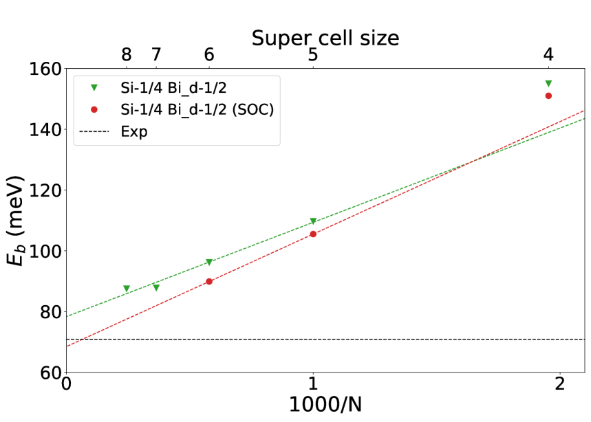
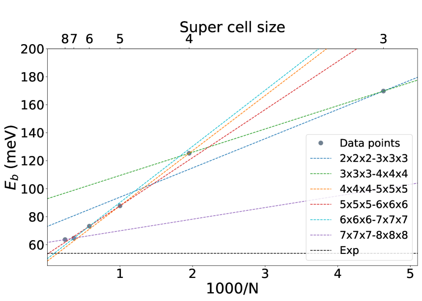
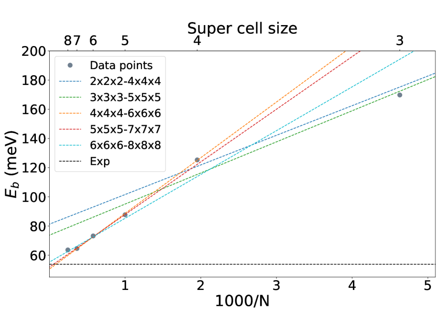
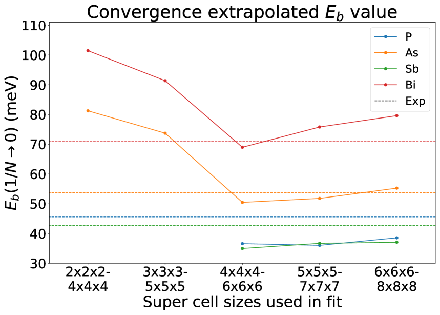
With Eq. (1) the binding energy of a single supercell size can be determined. To determine the binding energy of the isolated shallow donors, the results from various supercell sizes are extrapolated to an infinite system by fitting a linear curve through data points of , where is the number of atoms at the supercell. The final binding energy for the isolated donor is taking as the value at [7]. In appendix C, we investigate the convergence of the binding energy as a function of the supercell sizes used in the fit. We found that supercell sizes of and larger are needed for a precise prediction of the binding energy. Therefor, all our fits included at least the and supercell. The largest supercell size used in a fit can be found in Tab. 2.
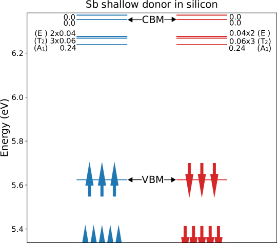
Given the small energy difference between the ground state shallow levels, excite state shallow levels and the CBM extra care must be taken be taken in regard with the smearing of a DFT calculation on the shallow level. We follow the procedure outlined by Swift et al. [7]. This procedure consist of two DFT calculations, an initial DFT calculation was performed using a small smearing value of eV followed by a calculation utilizing the SCF method [20] to enforce the occupation of a single shallow level. This ensures that the ground state shallow level () does not mix with higher energy shallow levels or conduction bands. In Fig. 1, we show an example of the mixing of shallow levels for an antimony dopant. We note that with our choice for the smearing in initial step, the second step rarely results in a different outcome for supercell sizes of or larger.
2.2 Constructing large supercells
To determine the binding energy, we did DFT calculation on supercell sizes ranging form the (64 atoms) to the (4096 atoms) supercell. Given the fact that the computational demand of the DFT- method is the same of the standard DFT method, the most significant bottleneck is the relaxation of the supercell, a step required in any calculation procedure. For large supercells, where a single ionic step can require tens of hours to several days, these relaxations become particularly burdensome. To still enable calculations on shallow defects within these larger systems, calculations crucial for accurately simulating them due to the extended nature of defect wavefunctions, we employed a strategy of embedding the supercell (1000 atoms) within a pristine silicon.
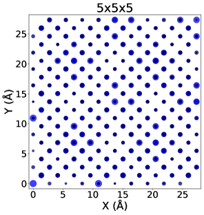
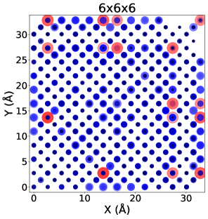
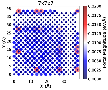
Fig. 2 depicts the maximum force acting on each atom within both the original, relaxed supercell and the embedded supercells within pristine silicon. We observe that at the interface between the relaxed supercell and the pristine silicon, the forces are indeed larger than those seen in the non-embedded case. However, the largest forces in the supercell is and for the (1728 atoms) and (2744 atoms), respectively. Although these values are an order of magnitude larger than the original convergence criterion of , they are roughly equal to the convergence criterion of commonly used in many works on defects in literature [21, 22, 23, 24]. Furthermore, previous studies [25] have indicated that the displacement of silicon atoms due to the creation of a vacancy becomes negligible when going from the to the supercells.
2.3 Computational details
The DFT calculations for this work utilized the Perdew-Burke-Ernzerhof (PBE) exchange correlation functional [26] and the Projector Augmented Wave (PAW) method [27], as implemented in the Vienna ab initio Simulation Package (VASP) [28, 29, 30]. Collinear spin polarization was included in all calculations unless otherwise noted. We determined the lattice parameter of bulk silicon using the Birch-Murnaghan equation of state [31], employing an energy cutoff of eV and a dense -point grid of in the Monkhorst-Pack scheme [32]. This yielded silicon-silicon interatomic distances and a lattice parameter of Å and Å, respectively, which is in good agreement with the experimentally determined lattice parameter of Å[33]. To determine the bulk DFT- correction for silicon, we followed the procedure outlined in [16] and removed 1/4th of an electron from the -orbital of silicon. We then determined the cutoff parameter by extremizing the band gap. The cutoff parameter was determined using a dense -point grid, which yielded a value of and a DFT- band gap of eV. These results align with previous DFT- calculations [16, 34], and the band gap is close to the experimentally measured value of eV [33]. The Kohn Sham potentials used to calculate the DFT- self-energy potentials were generated using a modified version of the atom code [35, 16].
| Donor | POTCAR type | ENCUT (eV) |
|---|---|---|
| P | 256 | |
| As | 246 | |
| As | _d | 289 |
| Sb | 246 | |
| Sb | _GW_d | 289 |
| Bi | 246 | |
| Bi | _d | 246 |
For the supercell sizes (64 atoms) and (216 atoms), a k-point grid of and was used respectively. For larger supercells, calculations were performed at the -point. The energy cutoff of all binding energy calculations can be found in Tab. 1. For structural relaxations, we used an energy cutoff scaled by a factor of 1.3 relative to these values.
3 Results
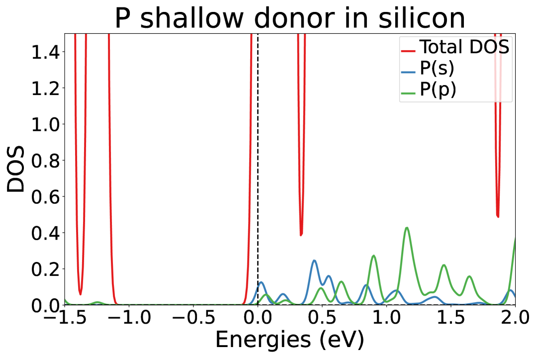
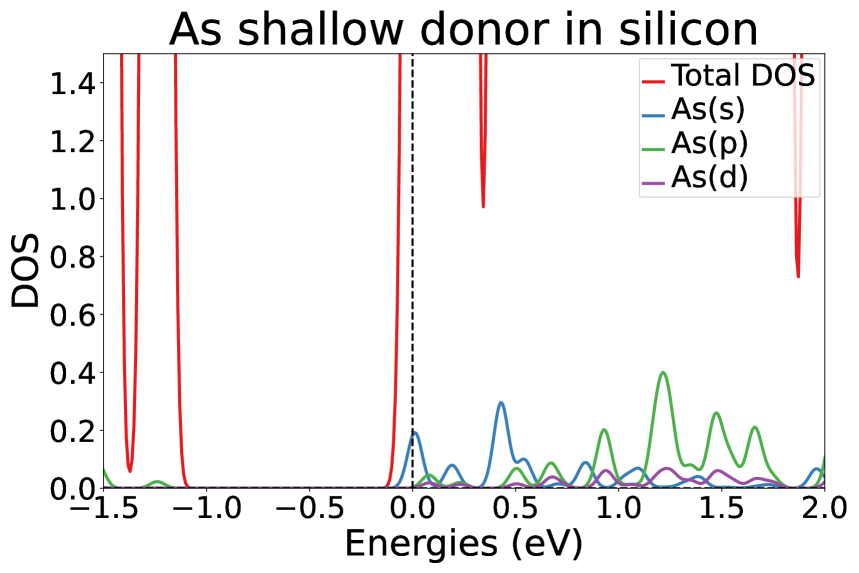
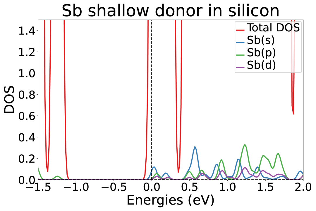
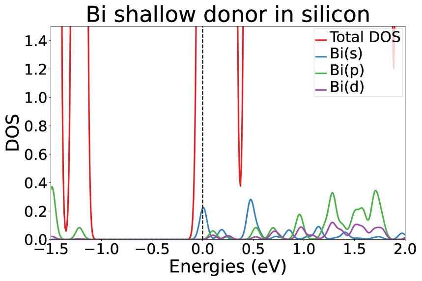
First, we apply the bulk DFT- correction to pristine silicon, resulting in an increased band gap of eV, which is in good agreement with the experimental value of eV, as discussed in Section 2.3. As a second step, we focus on the doped systems, where the bulk DFT- correction for silicon has already been incorporated. The first task in performing a DFT- calculation is to analyze the character of the highest occupied level, in this case, the impurity (shallow donor) level. To this end, we compute the total Density of States (DOS) and the Partial Density of States (PDOS) of the doped systems. Figure 3(d) presents these quantities for each group V donor (P, As, Sb, and Bi), including the PDOS of the donor atoms. Analysis of the PDOS reveals that the shallow donor level is primarily composed of silicon contributions, with additional weight from the donor -orbital in all cases. Based on this observation, we also apply the DFT- correction to the -orbital of the donor atom.
In Fig. 4(a) and 4(b), the binding energy is calculated for different supercell sizes, along with an extrapolation to the infinite supercell using both standard DFT, hereafter referred to simply as DFT, and DFT- , considering the different steps of correction, first with only the bulk silicon correction, denoted as Si, and after incorporating the effect of the donor atom, denoted as Si As. As expected, the DFT binding energy severely underestimates the experimental binding energy, due to the excessive delocalization of the wave functions inherent to the PBE functional. The bulk DFT- correction for Si increases the band gap, which results in an increase in the level separation between the shallow level and the CBM. This in turn results in an increased binding energy, bringing the prediction closer to the experimental results. Despite this improvement, the values from DFT- (Si) still are underestimated in comparison with the experimental [36] and tandem-HSE results from Ref. [7].
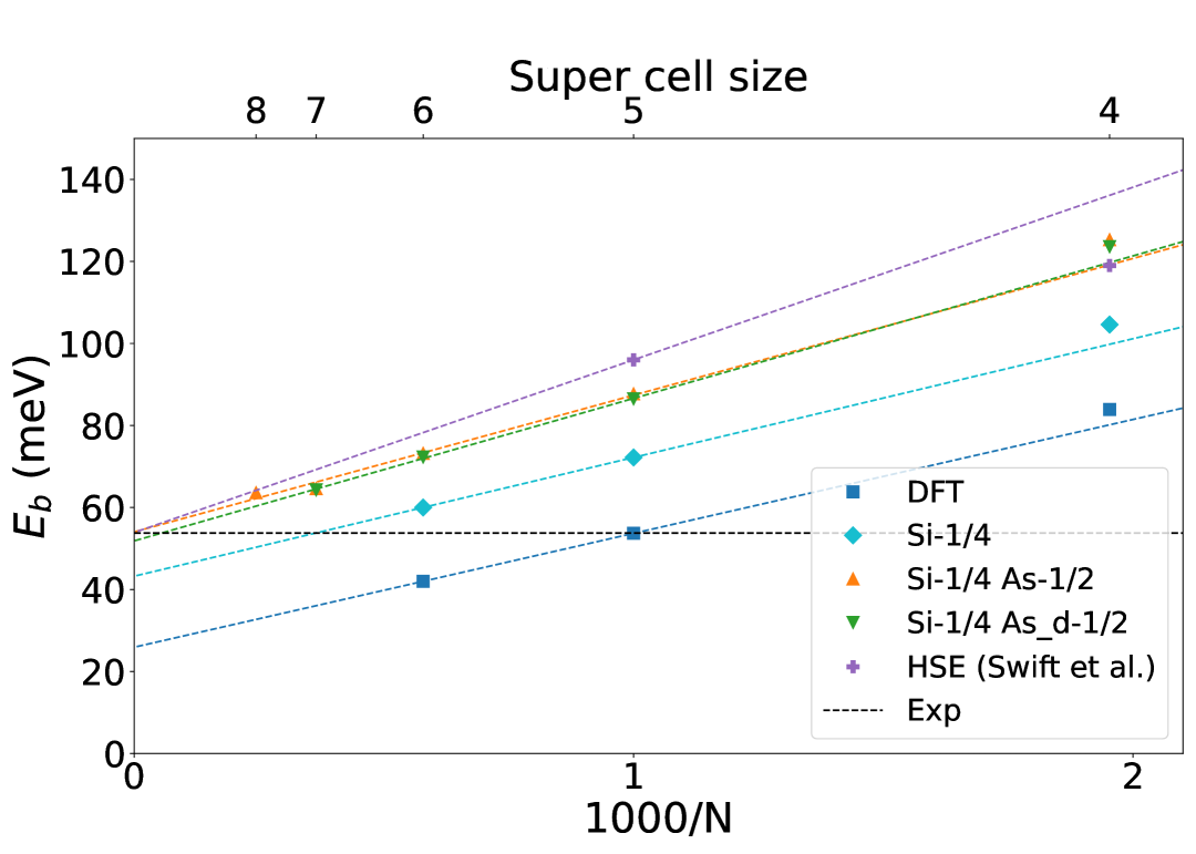
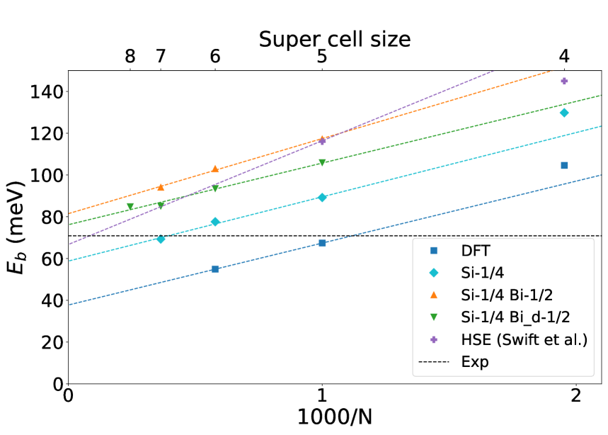
Part of the appeal of calculating binding energies with DFT, as opposed to the EMT, is that DFT incorporates the effect of the donor atom. It is therefore also reasonable that, when the DFT- method is used, all atoms should receive a correction. Following the DFT- approach, the self-energy potential is constructed by removing half an electron from a selected atomic orbital, thereby mimicking the effect of quasiparticle corrections.
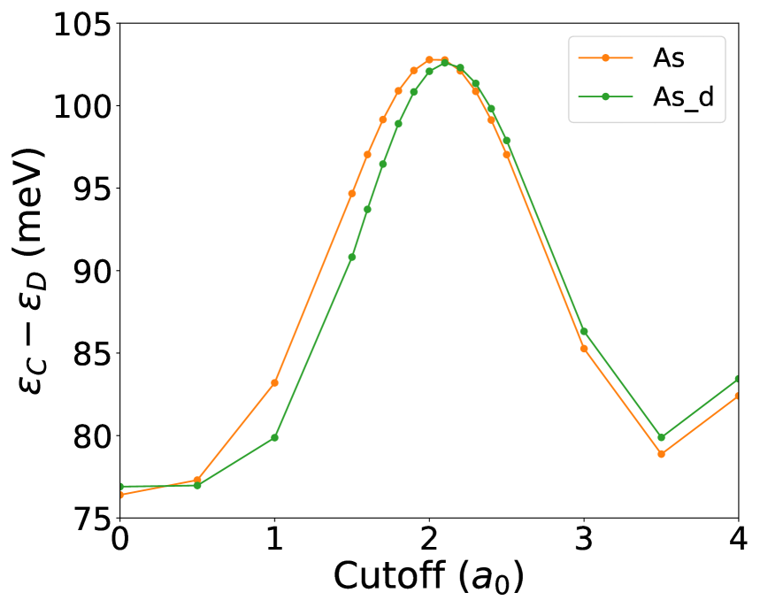
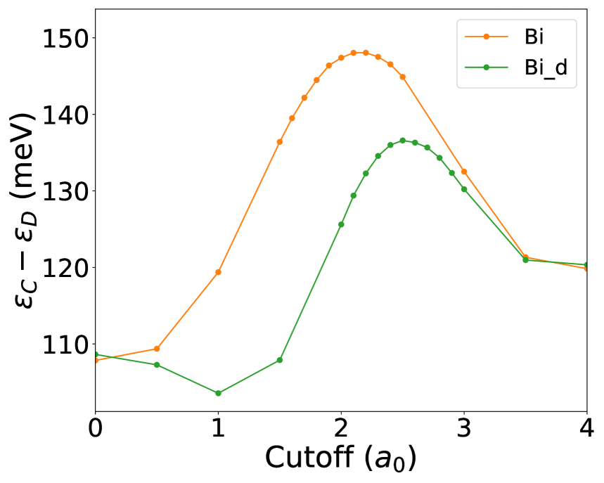
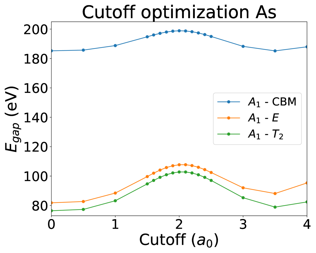
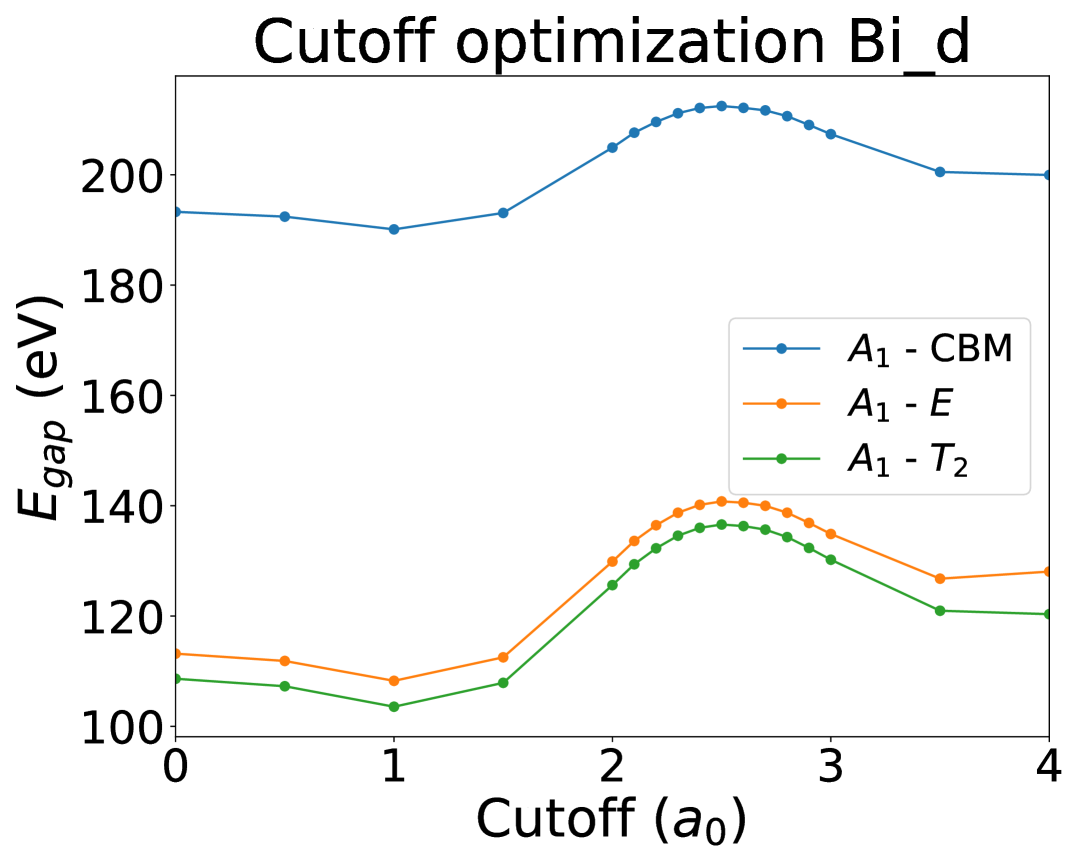
To apply the DFT- method to the shallow donor level, the corresponding half-electron potential must be removed, taking into account the orbital character of the shallow level, in this case the -orbital of the impurity. Denoting the shallow donor level by and the nearest unoccupied conduction band level of the same spin by , the optimal cutoff radius () is determined by maximizing the energy separation . The resulting optimization curves for different cutoff radii are shown in Fig. 5 for As and Bi within a supercell.
The donor corrections lead to an increase of the separation for the supercell size by approximately meV for As and meV for Bi, relative to the case with only the bulk silicon correction. Therefore the overall binding energy likely increases with the impurities correction. As shown in appendix B the cutoff parameters remain the same when increasing the supercell size beyond , confirming the transferability of the donor corrected potential, without requiring re-optimization for larger supercells.
The corrected potentials determined in Fig. 5, were then used to recalculate the binding energy for arsenic and bismuth. For arsenic, the corrected result yields a binding energy of meV, which is in excellent agreement with the experimental value of meV [37] (see Fig. 4(a) and Tab. 2). Similarly, the bismuth correction (Fig. 4(b)) increases the binding energy, though in this case the result of eV overestimates the experimental value by meV.
Our discussion thus far has focused on results obtained using pseudopotentials that treat -orbitals as core electrons. However, bismuth is a heavy atom, and the inclusion of -orbitals could be significant. After re-relaxing the defect with -valence orbitals, we determined the new cutoff parameter and corresponding DFT- potential, as shown in Fig. 5(b). The cutoff parameter and separation are noticeably affected, and consequently, the binding energy is likely to differ as well. Fig. 4(b) and Tab. 2 illustrate that the new binding energies are generally lower. After extrapolation, we obtain a binding energy of meV, bringing the calculated value closer to the experimental result of meV.
When including -valence orbitals for arsenic, the lighter element, no substantial change was observed in either the cutoff parameter or the final binding energy.
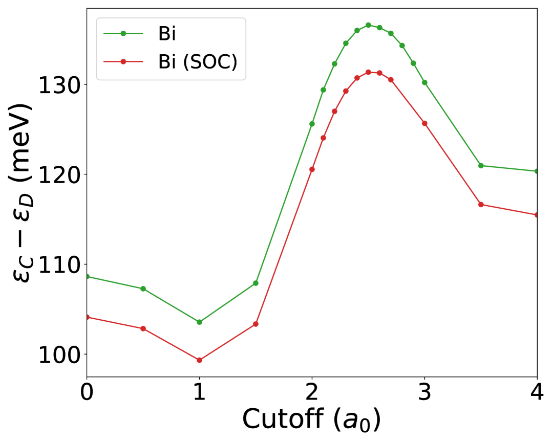
Nevertheless, even considering a more complete pseudopotential that includes -valence electrons, the binding energy for bismuth remains slightly overestimated. While the HSE result reported in Ref. [7] provides a closer match to the experimental value, it is important to note that those calculations did not include spin–orbit coupling (SOC), which is a critical relativistic effect for heavy atoms such as bismuth. To improve the accuracy of our prediction, we incorporated SOC in our calculations. As illustrated in Fig. 6(b), the inclusion of SOC leads to a reduction in the binding energy, improving agreement with the experimental value. After extrapolation , the binding energy for bismuth decreased from meV (without SOC) to meV (with SOC), aligning more closely with the experimental value of meV.
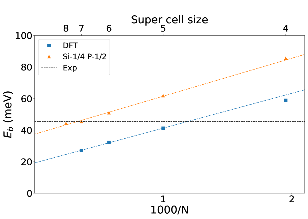
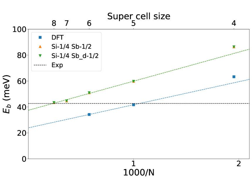
The procedure, as described above, was applied to the remaining group V donors in silicon, phosphorus (P) and antimony (Sb), as shown in Figs. 4(c) and 4(d). Because Sb is in between As and Bi in terms of size, the binding energy was determined with and without -valence orbitals. The inclusion of -valence orbitals altered the final binding energy by meV, although the difference is small it shows that generally the inclusion of -orbitals increases the accuracy of the calculation. For both P and Sb, we find that the DFT- consistently led to an increase in the calculated binding energy. With the exception of phosphorus, all methods predict binding energies within meV of the experimental value, that is if SOC is included for bismuth, while for phosphorus we find that the result deviates by meV.
We note that there is work in which the tandem HSE approach is used on phosphorus [24] with a prediction close to the experimental value. However, we expect that they overestimated the electrostatic potential alignment , as discussed in appendix D, and without this the HSE result would likely be inline with the DFT- results.
| Donor | Method | (Exp) | SC(max) | ||
| P | Si P | 19.20 | 45.58 | 22.07 | |
| Si-1/4 P-1/2 | 37.44 | 24.07 | |||
| As | Si As | 25.93 | 53.77 | 27.77 | |
| Si-1/4 As | 43.24 | 28.96 | |||
| Si-1/4 As-1/2 | 54.04 | 33.34 | |||
| Si-1/4 As_d-1/2 | 51.85 | 34.76 | |||
| HSE [7] | 53.9 | 42.1 | |||
| Sb | Si Sb_d | 23.90 | 42.71 | 17.80 | |
| Si-1/2 Sb-1/2 | 35.73 | 25.12 | |||
| Si-1/4 Sb_d-1/2 | 37.45 | 22.45 | |||
| Bi | Si Bi | 37.73 | 70.88 | 29.67 | |
| Si-1/4 Bi | 58.76 | 30.79 | |||
| Si-1/4 Bi-1/2 | 81.46 | 35.98 | |||
| Si-1/4 Bi_d-1/2 | 78.52 | 31.73 | |||
| Si-1/4 Bi_d-1/2 (SOC) | 66.25 | 42.25 | |||
| HSE [7] | 66.7 | 49.7 |
4 Conclusion
In this study, a comprehensive investigation of the effectiveness of the DFT- correction for accurately determining the binding energy for group V shallow donors in silicon is presented. Our approach systematically addresses the inherent limitations of standard DFT, such as band gap underestimation and electron delocalization errors, while crucially maintaining a high level of computational efficiency. We showed that it is essential to correct both the bulk silicon atoms and the donor atom. By doing so we found remarkable improvements upon the DFT results, which are known to severely underestimate binding energies. For arsenic, the calculated binding energy of meV is in excellent agreement with the experimental value of meV, differing by only approximately meV. This result is highly competitive with, and even slightly more accurate than, the HSE value of meV reported in the literature. For the bismuth donor, initial DFT- calculations without SOC overestimated the experimental value ( meV versus meV). However, by including SOC in our calculations, the binding energy significantly decreased to meV. This SOC-corrected value is remarkably close to the experimental value of meV, differing by approximately meV, and it is actually closer to the experimental value than the meV obtained with the computationally more demanding HSE functional. For the other Group V donors, antimony and phosphorus, the DFT-1/2 method also provided substantial improvements. For antimony, the binding energy prediction of meV is within approximately meV of the experimental value of meV. For phosphorus, while still an improvement, the result of meV deviates by approximately meV from the experimental value of meV.
Beyond its enhanced accuracy, the DFT- method offers a significant practical advantage, as being less complicated and less computationally demanding than other methods as HSE. While HSE calculations face limitations in supercell size due to large computational cost, the DFT- allowed us to perform calculations on supercells up to atoms, crucial for capturing the extended nature of shallow defect wavefunctions. We anticipate that this newly developed DFT-1/2 methodology can be generalized effectively to other shallow impurities in semiconductors.
In summary, the DFT-1/2 method represents a significant step forward in the ab initio simulation of shallow donors in silicon, providing highly accurate binding energies with a favorable computational cost, and offering a robust platform for further investigations into the electronic structure of these critical quantum systems.
Acknowledgements
This work was supported by the FWO (Research Foundation-Flanders), project G0D1721N. This work was performed in part using HPC resources from the VSC (Flemish Supercomputer Center) and the HPC infrastructure of the University of Antwerp (CalcUA), both funded by the FWO-Vlaanderen and the Flemish Government department EWI (Economie, Wetenschap & Innovatie).
References
- [1] P. Yu and M. Cardona “Fundamentals of Semiconductors: Physics and Materials Properties”, Graduate Texts in Physics Springer Berlin Heidelberg, 2010 URL: https://books.google.be/books?id=5aBuKYBT_hsC
- [2] B.K. Ridley “Quantum Processes in Semiconductors” OUP Oxford, 2013 URL: https://books.google.be/books?id=9ZIeAAAAQBAJ
- [3] W. Kohn and J.. Luttinger “Theory of Donor States in Silicon” In Phys. Rev. 98 American Physical Society, 1955, pp. 915–922 DOI: 10.1103/PhysRev.98.915
- [4] Gaigong Zhang et al. “Shallow Impurity Level Calculations in Semiconductors Using Ab Initio Methods” In Phys. Rev. Lett. 110 American Physical Society, 2013, pp. 166404 DOI: 10.1103/PhysRevLett.110.166404
- [5] A.M. Stoneham “Theory of Defects in Solids: Electronic Structure of Defects in Insulators and Semiconductors”, Oxford classic texts in the physical sciences Clarendon Press, 2001 URL: https://books.google.be/books?id=jUdrlVC9F0oC
- [6] Sokrates T. Pantelides “The electronic structure of impurities and other point defects in semiconductors” In Rev. Mod. Phys. 50 American Physical Society, 1978, pp. 797–858 DOI: 10.1103/RevModPhys.50.797
- [7] Michael W. Swift et al. “First-principles calculations of hyperfine interaction, binding energy, and quadrupole coupling for shallow donors in silicon” In npj Computational Materials 6.1, 2020, pp. 181 DOI: 10.1038/s41524-020-00448-7
- [8] Lin-Wang Wang “Density functional calculations of shallow acceptor levels in Si” In Journal of Applied Physics 105.12, 2009, pp. 123712 DOI: 10.1063/1.3153981
- [9] Paula Mori-Sánchez, Aron J. Cohen and Weitao Yang “Localization and Delocalization Errors in Density Functional Theory and Implications for Band-Gap Prediction” In Phys. Rev. Lett. 100 American Physical Society, 2008, pp. 146401 DOI: 10.1103/PhysRevLett.100.146401
- [10] Kyle R. Bryenton, Adebayo A. Adeleke, Stephen G. Dale and Erin R. Johnson “Delocalization error: The greatest outstanding challenge in density-functional theory” In WIREs Computational Molecular Science 13.2, 2023, pp. e1631 DOI: https://doi.org/10.1002/wcms.1631
- [11] H Peelaers et al. “Ab initio study of hydrogenic effective mass impurities in Si nanowires” In Journal of Physics: Condensed Matter 29.9 IOP Publishing, 2017, pp. 095303 DOI: 10.1088/1361-648X/aa5768
- [12] Bruno Lucatto et al. “General procedure for the calculation of accurate defect excitation energies from DFT-1/2 band structures: The case of the center in diamond” In Phys. Rev. B 96 American Physical Society, 2017, pp. 075145 DOI: 10.1103/PhysRevB.96.075145
- [13] Filipe Matusalem, Ronaldo R. Pelá, Marcelo Marques and Lara K. Teles “Charge transition levels of Mn-doped Si calculated with the GGA-1/2 method” In Phys. Rev. B 90 American Physical Society, 2014, pp. 224102 DOI: 10.1103/PhysRevB.90.224102
- [14] Filipe Matusalem et al. “Combined LDA and LDA-1/2 method to obtain defect formation energies in large silicon supercells” In Phys. Rev. B 88 American Physical Society, 2013, pp. 224102 DOI: 10.1103/PhysRevB.88.224102
- [15] Joshua Claes, Bart Partoens and Dirk Lamoen “Decoupled DFT- method for defect excitation energies” In Phys. Rev. B 108 American Physical Society, 2023, pp. 125306 DOI: 10.1103/PhysRevB.108.125306
- [16] Luiz G. Ferreira, Marcelo Marques and Lara K. Teles “Approximation to density functional theory for the calculation of band gaps of semiconductors” In Phys. Rev. B 78 American Physical Society, 2008, pp. 125116 DOI: 10.1103/PhysRevB.78.125116
- [17] Luiz G. Ferreira, Marcelo Marques and Lara K. Teles “Slater half-occupation technique revisited: the LDA-1/2 and GGA-1/2 approaches for atomic ionization energies and band gaps in semiconductors” In AIP Advances 1.3, 2011, pp. 032119 DOI: 10.1063/1.3624562
- [18] Chris G. Walle and Jörg Neugebauer “First-principles calculations for defects and impurities: Applications to III-nitrides” In Journal of Applied Physics 95, 2004, pp. 3851–3879 URL: https://api.semanticscholar.org/CorpusID:17667822
- [19] M.. Amini, R. Saniz, D. Lamoen and B. Partoens “Hydrogen impurities and native defects in CdO” In Journal of Applied Physics 110.6, 2011, pp. 063521 DOI: 10.1063/1.3641971
- [20] Adam Gali et al. “Theory of Spin-Conserving Excitation of the Center in Diamond” In Phys. Rev. Lett. 103 American Physical Society, 2009, pp. 186404 DOI: 10.1103/PhysRevLett.103.186404
- [21] Gergő Thiering and Adam Gali “Ab Initio Magneto-Optical Spectrum of Group-IV Vacancy Color Centers in Diamond” In Phys. Rev. X 8 American Physical Society, 2018, pp. 021063 DOI: 10.1103/PhysRevX.8.021063
- [22] I-Te Lu, Jin-Jian Zhou and Marco Bernardi “Efficient ab initio calculations of electron-defect scattering and defect-limited carrier mobility” In Phys. Rev. Mater. 3 American Physical Society, 2019, pp. 033804 DOI: 10.1103/PhysRevMaterials.3.033804
- [23] Mark E. Turiansky, Audrius Alkauskas, Lee C. Bassett and Chris G. Van de Walle “Dangling Bonds in Hexagonal Boron Nitride as Single-Photon Emitters” In Phys. Rev. Lett. 123 American Physical Society, 2019, pp. 127401 DOI: 10.1103/PhysRevLett.123.127401
- [24] Hongyang Ma et al. “Ab-initio calculations of shallow dopant qubits in silicon from pseudopotential and all-electron mixed approach” In Communications Physics 5.1, 2022, pp. 165 DOI: 10.1038/s42005-022-00948-6
- [25] Vladislav Pelenitsyn and Pavel Korotaev “First-principles study of radiation defects in silicon” In Computational Materials Science 207, 2022, pp. 111273 DOI: https://doi.org/10.1016/j.commatsci.2022.111273
- [26] John P. Perdew, Kieron Burke and Matthias Ernzerhof “Generalized Gradient Approximation Made Simple” In Phys. Rev. Lett. 77 American Physical Society, 1996, pp. 3865–3868 DOI: 10.1103/PhysRevLett.77.3865
- [27] G. Kresse and D. Joubert “From ultrasoft pseudopotentials to the projector augmented-wave method” In Phys. Rev. B 59 American Physical Society, 1999, pp. 1758–1775 DOI: 10.1103/PhysRevB.59.1758
- [28] G. Kresse and J. Hafner “Ab initio molecular-dynamics simulation of the liquid-metal–amorphous-semiconductor transition in germanium” In Phys. Rev. B 49 American Physical Society, 1994, pp. 14251–14269 DOI: 10.1103/PhysRevB.49.14251
- [29] G. Kresse and J. Furthmüller “Efficiency of ab-initio total energy calculations for metals and semiconductors using a plane-wave basis set” In Computational Materials Science 6.1, 1996, pp. 15–50 DOI: https://doi.org/10.1016/0927-0256(96)00008-0
- [30] G. Kresse and J. Furthmüller “Efficient iterative schemes for ab initio total-energy calculations using a plane-wave basis set” In Phys. Rev. B 54 American Physical Society, 1996, pp. 11169–11186 DOI: 10.1103/PhysRevB.54.11169
- [31] Francis Birch “Finite Elastic Strain of Cubic Crystals” In Phys. Rev. 71 American Physical Society, 1947, pp. 809–824 DOI: 10.1103/PhysRev.71.809
- [32] Hendrik J. Monkhorst and James D. Pack “Special points for Brillouin-zone integrations” In Phys. Rev. B 13 American Physical Society, 1976, pp. 5188–5192 DOI: 10.1103/PhysRevB.13.5188
- [33] Madelung Otfried “Semiconductors - Basic Data” Springer, 1996
- [34] Jan Doumont, Fabien Tran and Peter Blaha “Limitations of the DFT-1/2 method for covalent semiconductors and transition-metal oxides” In Phys. Rev. B 99 American Physical Society, 2019, pp. 115101 DOI: 10.1103/PhysRevB.99.115101
- [35] José M Soler et al. “The SIESTA method for ab initio order-N materials simulation” In Journal of Physics: Condensed Matter 14.11 IOP Publishing, 2002, pp. 2745–2779 DOI: 10.1088/0953-8984/14/11/302
- [36] A L Saraiva, A Baena, M J Calderón and Belita Koiller “Theory of one and two donors in silicon” In Journal of Physics: Condensed Matter 27.15 IOP Publishing, 2015, pp. 154208 DOI: 10.1088/0953-8984/27/15/154208
- [37] HG Grimmeiss, E Janzén and K Larsson “Multivalley spin splitting of 1s states for sulfur, selenium, and tellurium donors in silicon” In Physical Review B 25.4 APS, 1982, pp. 2627
- [38] Bernard Pajot “Optical Absorption of Impurities and Defects in Semiconducting Crystals: Hydrogen-like Centres” Springer Science & Business Media, 2010
- [39] Hongyang Ma et al. “Dataset: Ab-initio calculations of shallow dopant qubits in silicon from pseudopotential and all-electron mixed approach”, 2022 DOI: https://dx.doi.org/10.17172/NOMAD/2022.06.25-1
- [40] Christoph Freysoldt, Jörg Neugebauer and Chris Van Walle “Fully Ab Initio Finite-Size Corrections for Charged-Defect Supercell Calculations” In Phys. Rev. Lett. 102, 2009, pp. 016402 DOI: 10.1103/PhysRevLett.102.016402
- [41] Christoph Freysoldt, Jörg Neugebauer and Chris G. Van de Walle “Electrostatic interactions between charged defects in supercells” In physica status solidi (b) 248.5, 2011, pp. 1067–1076 DOI: https://doi.org/10.1002/pssb.201046289
Appendix A The energy cutoff
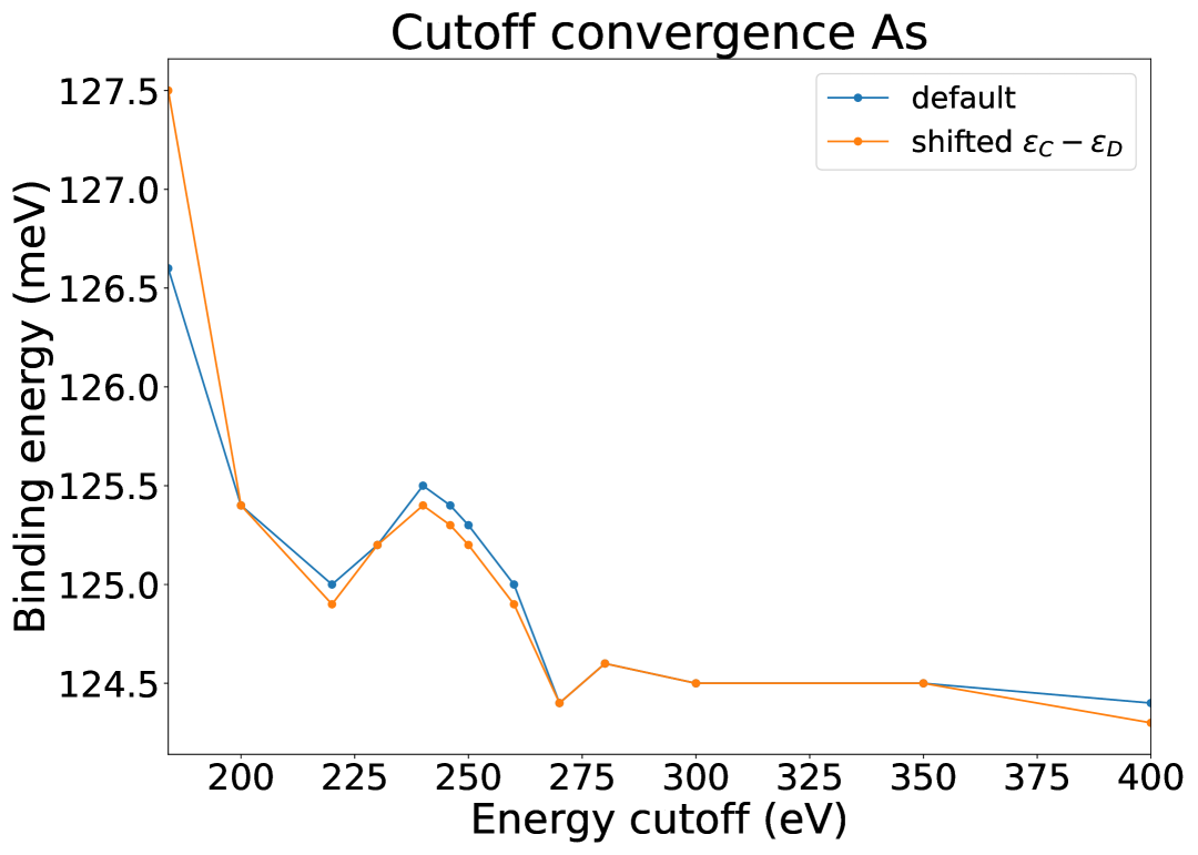
In the main text, we use the energy cutoff values shown in Tab. 1. In most cases, the energy cutoff was set to the highest ENMAX value from the POTCAR file for the system. Since the binding energy is a very small value, a low energy cutoff can significantly affect the reliability of the calculation. Figure 7(a) examines the convergence of the binding energy as a function of the energy cutoff. The chosen energy cutoff of 246 eV differs by only approximately meV from the largest cutoff value of eV.
The same figure also compares the convergence of the binding energy with that of the separation , which is the gap between the shallow level and the conduction band of the same spin right above. The separation in the doped system appears to serve as a convergence criterion. This is convenient because it means we don’t need to calculate the pristine system at each tested energy cutoff.
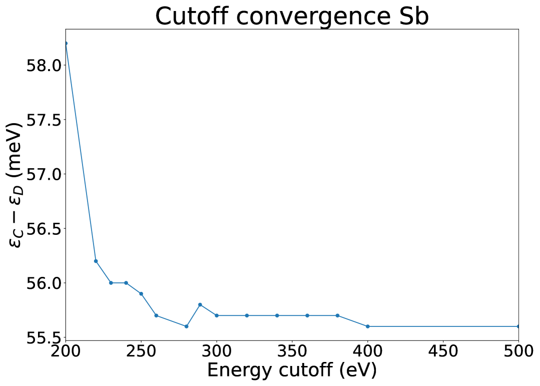
Fig. 7(b) checks the energy cutoff convergence for antimony. For this system, seems to converge well before the ENMAX value of 289 eV.
Appendix B DFT- cutoff parameter convergence
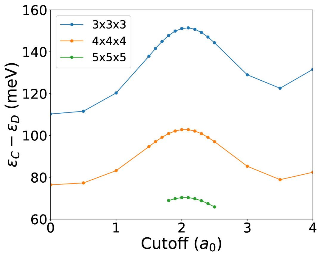
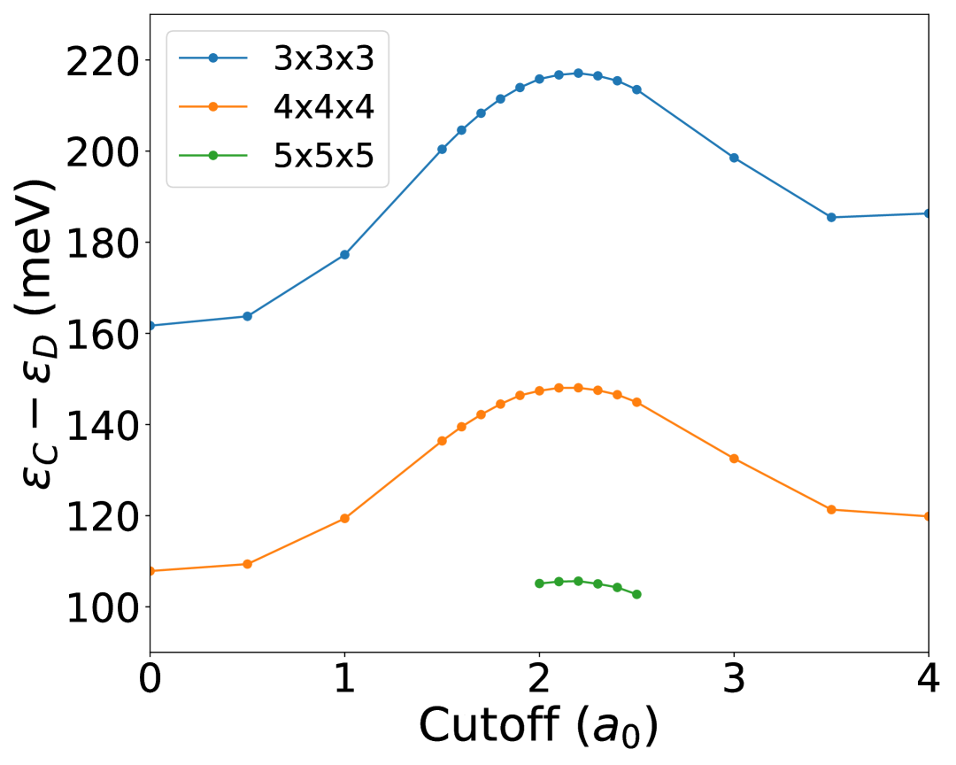
To maintain the efficiency of the shallow defect calculation procedure, it would be ideal if the cutoff radius, , could be determined on a small supercell. This would minimize the number of calculations required for the large supercell. We therefore checked the convergence of the cutoff parameter for different supercell sizes, as shown in Fig. 8 and Tab. 3. The cutoff parameter seems to converge rather quickly, and a supercell size of is sufficient to correctly determine this parameter.
| Supercell | As | Bi | ||
|---|---|---|---|---|
| 2.1 | 151.4 | 2.2 | 217.0 | |
| 2.0 | 102.8 | 2.2 | 148.1 | |
| 2.0 | 70.3 | 2.2 | 105.6 | |
A challenge when dealing with shallow defects lies in selecting the appropriate gap to optimize. Typically, bulk calculations focus on maximizing the gap between the highest occupied and lowest unoccupied levels, the band gap. However, in our calculations, directly maximizing this would optimize the gap between the occupied shallow level and the unoccupied shallow level. Instead, we are interested in the binding energy, which represents the gap between the level and the Conduction Band Minimum (CBM)111If the shallow level is at index , we need to optimize the gap between and to obtain the gap between and the CBM. Figure 9 illustrates the various gaps between the shallow level and other shallow levels, as well as the gap with the CBM, during the optimization process for the cutoff parameter. We observed that optimizing for any of these gaps leads to cutoff parameters within of each other. For the , an error of in the cutoff parameter results in an error of at most meV in the seperation and this error decreases with supercell size. For example for the supercell this error is at most meV. Given the close proximity of all gaps shown in Fig. 9, we selected the gap to determine the cutoff parameter, maintaining consistency with the typical bulk method.
Appendix C Convergence of binding energy calculations
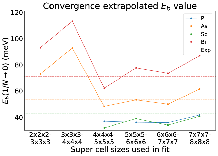
To efficiently apply the DFT- method for binding energies, it is important to know which supercell sizes should be included in the fit predict the binding accuracy accurately. In Fig. 10 the fits and predict binding energies are shown for different supercell sizes. In seems like the binding energy converges for fits with supercell sizes of or higher. However, a closer look at Fig. 4 and 6(b) shows that the binding energy of the still significantly deviates from the actual fits. We therefor chose to ignore this point in all our fits and started fitting with the supercells and larger. But we do note that the and can already yield a reasonable prediction for the final value.
If we focus on the fits of the two largest supercell size i.e. and in Fig. 10(a) and 10(b), we notice that the prediction is off. This is likely due to small numerical error for the predicted binding energy, to which the larger supercells are more sensitive, combined with a small difference in value resulting incorrect prediction for the final binding energy. Therefor it is important to also include the fits of the smaller supercell sizes of and .
Appendix D Literature HSE result for Phosphorus
It remains unclear why the DFT- results for the P dopant exhibit lower accuracy compared to the other dopants. We note that there is a work in literature by Ma et al. [24] which determines the binding energy with the tandem HSE approach for P, thereby providing DFT calculations against which we can compare our results. When comparing our DFT binding energy with those of [24], we observe that our binding energy of meV is significantly lower than their prediction of meV.
Had our DFT result been closer to their value, it is likely that our final DFT- prediction would better align with experimental data. All binding energies for specific supercell sizes and intermediate results from these calculations can be found in Appendix E.
However, we suspect that the predicted values by Ma et al. are inaccurate. Given that their input files are publicly available [39], we attempted to reproduce the binding energy for the and supercells. Despite the availability of their input files, we were unable to recreate their reported binding energies of meV and meV, consistently obtaining binding energies of meV and meV for the and supercells, respectively. This aligns with our result of meV and meV, but not with the published values. Upon closer inspection, our values for and (see Tab. 4) are in agreement222They differ by less than meV, consistent with the precision of the results presented in [24]. with those found in the supplemental material of [24] (also shown in Tab. 5).
However, the electrostatic energy shift differs significantly between our calculations. We find a value of meV for the , while they report meV, which roughly 50% of their calculated binding energy. We determined using both the histogram method (as described in the main text) and the tetrahedron method [19], both yielding the aforementioned result of meV333This result is anticipated, as the methods are equivalent. Additionally, we employed the method of Freysoldt et al. [40, 41], the methodology used in [24], which resulted in a value of meV.
Furthermore, comparing the values of for arsenic and bismuth with those reported in the article by Swift et al. [7], we find that our values differ by at most meV, attributable to slight variations in the computational setup and the use of the method by Freysoldt for calcualting by Swift et al.
Given these discrepancies, we suspect that Ma et al. may have incorrectly calculated the values for , and that their agreement with experiment is coincidental444We have only examined the VASP inputs and not the CP2k inputs used in this work. However, both methodologies yield comparable values for . Therefore, the predicted value for using the tandem HSE approach is likely overestimated, suggesting that the tandem HSE predictions aligns more closely with our DFT- results.
| Supercell | |||
|---|---|---|---|
| 6.294 | 6.246 | 0.024 | |
| 6.269 | 6.242 | 0.016 |
| Supercell | |||
|---|---|---|---|
| 6.294 | 6.246 | 0.044 | |
| 6.269 | 6.242 | 0.037 |
Appendix E Intermediate results binding energies
| Method | Supercell | ||||
|---|---|---|---|---|---|
| Si P | 6.2801 | 6.2357 | 0.0145 | 0.0589 | |
| 6.2466 | 6.2219 | 0.0165 | 0.0412 | ||
| 6.2389 | 6.2212 | 0.0145 | 0.0322 | ||
| 6.2418 | 6.2272 | 0.0125 | 0.0271 | ||
| Si-1/4 P-1/2 | 6.3895 | 6.3195 | 0.0155 | 0.0855 | |
| 6.3671 | 6.3218 | 0.0165 | 0.0618 | ||
| 6.3659 | 6.3294 | 0.0145 | 0.0510 | ||
| 6.3733 | 6.3394 | 0.0115 | 0.0454 | ||
| 6.3736 | 6.3379 | 0.0085 | 0.0442 |
| Method | Supercell | ||||
|---|---|---|---|---|---|
| Si As | 6.3876 | 6.0953 | -0.0045 | 0.2878 | |
| 6.3876 | 6.2307 | 0.0175 | 0.1744 | ||
| 6.2843 | 6.2169 | 0.0165 | 0.0839 | ||
| 6.2508 | 6.2116 | 0.0145 | 0.0537 | ||
| 6.2431 | 6.2146 | 0.0135 | 0.0420 | ||
| Si-1/4 As | 6.5395 | 6.1939 | 0.0145 | 0.3601 | |
| 6.5824 | 6.4640 | 0.0165 | 0.1349 | ||
| 6.3940 | 6.3099 | 0.0205 | 0.1046 | ||
| 6.3715 | 6.3158 | 0.0165 | 0.0722 | ||
| 6.3704 | 6.3249 | 0.0145 | 0.0600 | ||
| Si-1/4 As-1/2 | 6.5395 | 6.1214 | -0.0185 | 0.3996 | |
| 6.5824 | 6.4261 | 0.0135 | 0.1698 | ||
| 6.3940 | 6.2852 | 0.0165 | 0.1253 | ||
| 6.3715 | 6.2973 | 0.0135 | 0.0877 | ||
| 6.3704 | 6.3087 | 0.0115 | 0.0732 | ||
| 6.3764 | 6.3193 | 0.0075 | 0.0646 | ||
| 6.3736 | 6.3155 | 0.0055 | 0.0636 | ||
| Si-1/4 As_d-1/2 | 6.3832 | 6.2721 | 0.0125 | 0.1236 | |
| 6.3607 | 6.2857 | 0.0115 | 0.0865 | ||
| 6.3594 | 6.2976 | 0.0105 | 0.0723 | ||
| 6.3653 | 6.3085 | 0.0075 | 0.0643 |
| Method | Supercell | ||||
|---|---|---|---|---|---|
| Si Sb_d | 6.2738 | 6.2370 | 0.0265 | 0.0633 | |
| 6.2402 | 6.2180 | 0.0195 | 0.0417 | ||
| 6.2324 | 6.2157 | 0.0175 | 0.0342 | ||
| Si-1/2 Sb-1/2 | 6.3940 | 6.3414 | 0.0355 | 0.0881 | |
| 6.3715 | 6.3346 | 0.0235 | 0.0604 | ||
| 6.3704 | 6.3393 | 0.0205 | 0.0516 | ||
| 6.3764 | 6.3469 | 0.0145 | 0.0440 | ||
| Si-1/2 Sb_d-1/2 | 6.3832 | 6.3263 | 0.0295 | 0.0864 | |
| 6.3607 | 6.3214 | 0.0205 | 0.0598 | ||
| 6.3594 | 6.3269 | 0.0185 | 0.0510 | ||
| 6.3653 | 6.3351 | 0.0145 | 0.0447 | ||
| 6.3736 | 6.3407 | 0.0105 | 0.0434 |
| Method | Supercell | ||||
|---|---|---|---|---|---|
| Si Bi | 6.3876 | 6.0951 | 0.0745 | 0.3670 | |
| 6.3876 | 6.3554 | 0.0275 | 0.0597 | ||
| 6.2843 | 6.2042 | 0.0245 | 0.1046 | ||
| 6.2508 | 6.2019 | 0.0185 | 0.0674 | ||
| 6.2431 | 6.2047 | 0.0165 | 0.0549 | ||
| Si-1/4 Bi | 6.5395 | 6.1932 | 0.0665 | 0.4128 | |
| 6.5824 | 6.4417 | 0.0295 | 0.1702 | ||
| 6.3940 | 6.2917 | 0.0275 | 0.1298 | ||
| 6.3715 | 6.2998 | 0.0175 | 0.0892 | ||
| 6.3704 | 6.3083 | 0.0155 | 0.0776 | ||
| 6.3764 | 6.3176 | 0.0105 | 0.0693 | ||
| Si-1/4 Bi-1/2 | 6.5395 | 6.1153 | 0.0705 | 0.4947 | |
| 6.5824 | 6.3878 | 0.0275 | 0.2221 | ||
| 6.3940 | 6.2528 | 0.0225 | 0.1637 | ||
| 6.3715 | 6.2688 | 0.0145 | 0.1172 | ||
| 6.3704 | 6.2799 | 0.0125 | 0.1030 | ||
| 6.3764 | 6.2898 | 0.0075 | 0.0941 | ||
| Si-1/4 Bi_d-1/2 | 6.3940 | 6.2677 | 0.0285 | 0.1548 | |
| 6.3715 | 6.2781 | 0.0175 | 0.1109 | ||
| 6.3704 | 6.2879 | 0.0135 | 0.0960 | ||
| 6.3764 | 6.2974 | 0.0095 | 0.0885 | ||
| 6.3857 | 6.3041 | 0.0065 | 0.0881 | ||
| Si-1/4 Bi_d-1/2 (SOC) | 6.3940 | 6.2707 | 0.0265 | 0.1498 | |
| 6.3715 | 6.2805 | 0.0175 | 0.1085 | ||
| 6.3704 | 6.2902 | 0.0105 | 0.0907 |