Wireless Josephson parametric amplifier above 20 GHz
Abstract
Operating superconducting qubits at elevated temperatures offers increased cooling power and thus system scalability, but requires suppression of thermal photons to preserve coherence and readout fidelity. This motivates migration to higher operation frequencies, which demands high-frequency amplification with near-quantum-limited noise characteristics for qubit readout. Here, we report the design and experimental realization of a wireless Josephson parametric amplifier (WJPA) operating above 20 GHz. The wireless design eliminates losses and impedance mismatches that become problematic at high frequencies. The WJPA achieves more than 20 dB of gain across a tunable frequency range of 21–23.5 GHz, with a typical dynamic bandwidth of 3 MHz. Through Y-factor measurements and a qubit-based photon number calibration, we show that the amplifier exhibits an added noise of approximately two photons.
I Introduction
Conventional superconducting qubit platforms for large-scale quantum computation Google Quantum AI and Collaborators (2025); Gao et al. (2025) employ sub-10 GHz qubits operating below 20 mK in dilution refrigerators. At these temperatures, limited cooling power presents a significant challenge to scalability. Raising the operating temperature to the range of 100 mK–1 K offers substantially greater cooling headroom, enabling the operation of more qubits. However, this increase in temperature also elevates the excited-state population of sub-10 GHz qubits, necessitating more complex state preparation protocols such as autonomous coolingMagnard et al. (2018) or measurement-based resetJohnson et al. (2012). Additionally, thermal population in sub-10 GHz readout resonators contributes to qubit dephasing via photon shot noiseKrantz et al. (2019).
To mitigate these effects, circuit QED systems operating at elevated temperatures must also transition to higher frequencies—typically in the 20–100 GHz range. Recent studies have demonstrated qubits operating above 20 GHz using advanced Josephson junctions and weak-links with superconducting Nb Anferov et al. (2024a, 2025) and TiN Purmessur et al. (2025). In parallel, readout resonators are also being pushed to higher frequencies to suppress thermal photon-induced dephasing. High-frequency resonators coupled to conventional frequency qubits are also under active investigation, as large detuning between qubit and readout frequencies can reduce measurement-induced state transitions, thereby enhancing readout fidelity and repeatability Swiadek et al. (2024); Nesterov and Pechenezhskiy (2024); Kurilovich et al. (2025). These developments collectively call for the development of ultra-low-noise amplification systems operating above 20 GHz to enable fast, high-fidelity qubit readout.
State-of-the-art superconducting qubit measurement chains typically employ Josephson parametric amplifiers (JPAs) as the first stage of nearly quantum-limited amplification Aumentado (2020); Roy and Devoret (2016). However, conventional JPA designs operating below 12 GHz face significant challenges when scaled to higher frequencies. Standard packaging techniques—such as wirebonding JPA chips to printed circuit boards (PCBs)—introduce loss and impedance mismatches that worsen at high frequencies. Moreover, parasitic modes in these packages can interfere with the JPA mode and degrade noise performance. While some of these limitations can be mitigated Anferov et al. (2024a), scaling beyond 20 GHz is more readily achieved with designs that eliminate wirebonds and lossy PCB materials altogether. A promising precedent was established by Narla et al. Narla et al. (2014), who demonstrated a wireless JPA coupling scheme using a rectangular waveguide to realize parametric amplification at 10.2 GHz and below. In this work, we show that such wireless coupling schemes can be extended to realize parametric amplification at higher frequencies required for next-generation circuit QED systems.
We report the design and characterization of a wireless Josephson parametric amplifier (WJPA) that operates in the K-band (18–26 GHz). The device, realized with aluminum/aluminum-oxide JJs, achieved more than 20 dB of gain over a tunable frequency range of 21 to 23.5 GHz, with an average dynamic bandwidth of 3 MHz. The WJPA, operated as a single pump four-wave mixing amplifier, achieved a 1 dB input compression power at 20 dB gain of dBm. Using Y-factor and qubit-based photon number calibration techniques, the system added noise with the WJPA was measured to be approximately two photons at 22 GHz.
II WJPA device design and fabrication
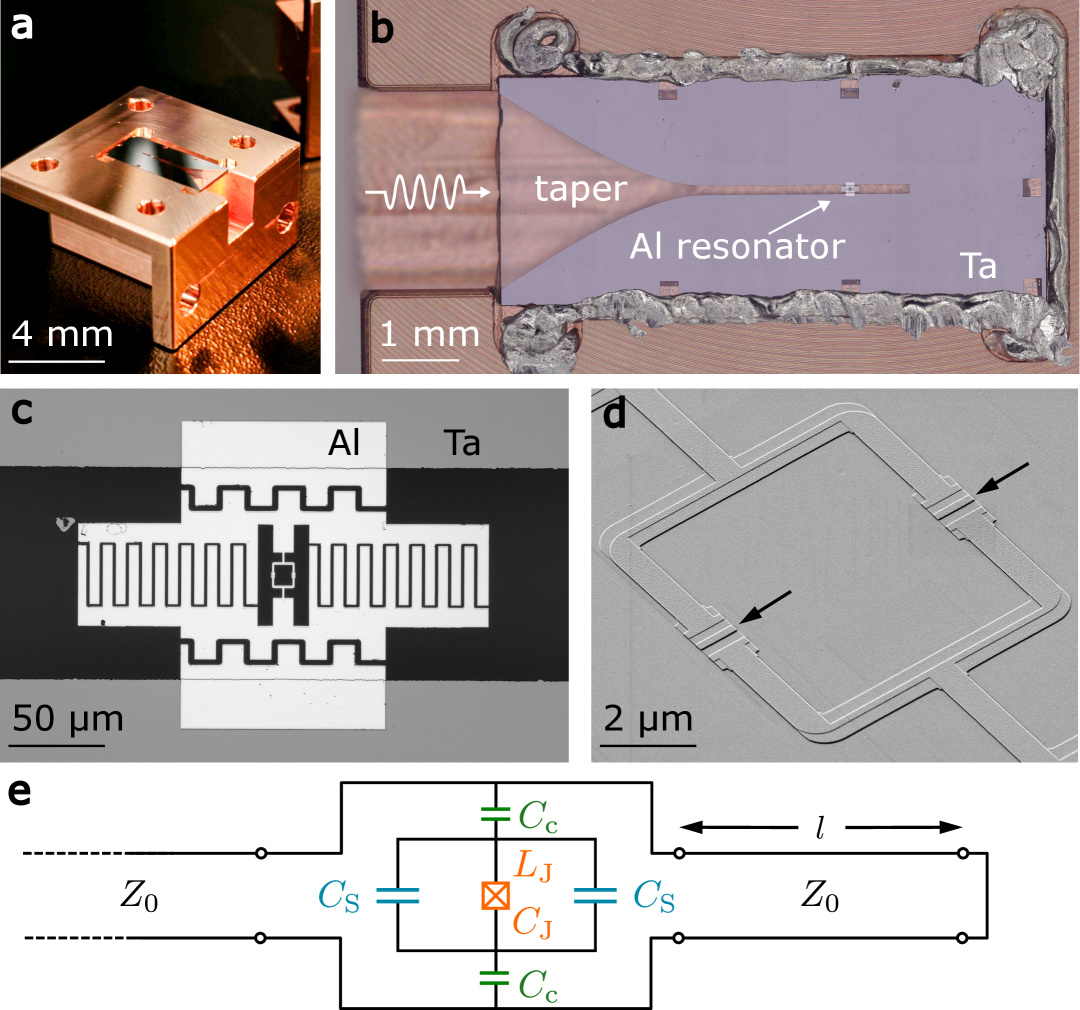
The WJPA device is shown in Fig. 1(a-d), with equivalent circuit diagram depicted in Fig. 1(e). The device is realized by a planar on-chip circuit mounted in a 3D copper package, with microwave signals applied through a rectangular waveguide launch. The rectangular waveguide dimensions were chosen to be 10.67 mm by 4.32 mm, corresponding to the WR42 standard rectangular waveguide specification, for frequency range of 18 to 26 GHz (K-band). The package is designed to be attached to a commercial WR42-2.92mm coaxial cable adapter (not shown) which is then connected to other microwave components. Fig. 1(b) shows a top view of the chip sitting in the copper package where the left opening mates with the WR42 adapter. Inspired by previous work on millimeter-wave superconducting circuits Anferov et al. (2024b, 2025), this design avoids wirebonds by using a lithographically defined transition from the waveguide to a slotline transmission line. The transition takes the form from Anferov et al. Anferov et al. (2025), where is the smaller rectangular waveguide dimension (4.32 mm for WR42), is the slotline gap width, and mm is the transition length in our optimized design. With electromagnetic simulation in Ansys HFSS, the taper was found to have a return loss below 10 dB and insertion loss under 1 dB over the target frequency band of 18 to 26 GHz. The slotline, defined on a sapphire substrate with superconducting ground planes, was designed with a gap width = 200 m, yielding a characteristic impedance of approximately . The slotline is shorted at one end, and a tunable lumped-element resonator is capacitively coupled at a distance mm, corresponding to a quarter-wavelength at frequency of approximately GHz.
An optical micrograph of the lumped-element resonator are shown in Fig. 1(c). The resonator is composed of an Al/AlOx Josephson junction (JJ) SQUID and interdigitated finger capacitors . The lithographically defined coupling capacitors were designed to achieve a coupling quality factor Q 100, and corresponding coupling rate 200 MHz. In electromagnetic simulations, we found variation of when varying the Josephson inductance from 100 to 200 pH. Crucially, we found that the junction capacitance , often ignored in lower frequency applications, must be taken into account for higher-frequency designs. This is because becomes comparable to as the targeted resonant frequency approaches the JJ plasma frequency, GHz.
Additionally, the junction participation ratio is a crucial parameter for ensuring that this nonlinear resonator can operate reliably as a parametric amplifier for amplifying signals from qubits. Here corresponds to the effective inductance of the resonant mode, which includes the contribution of the non-negligible parasitic inductance of the shunt capacitors. As described in supplementary Sec. I, we estimate from black-box quantization analysis of the simulated admittance Manucharyan et al. (2007); Nigg et al. (2012); Frattini et al. (2018). This gives a quality factor-participation ratio product , which ensures, according to previous results, that the device should reliably achieve gain dB Manucharyan et al. (2007); Narla et al. (2014); Schackert (2013).
The key benefits of our WJPA design for high-frequency operation are three-fold: First, the waveguide launch simplifies packaging and reduces the losses present in circuit-board-based packages, which get worse at high frequency. Second, the wireless coupling scheme avoids impedance mismatches introduced by wire-bonds to the circuit board that also become problematic at high frequencies as they cause uncontrolled variation of . Third, the planar nature of the resonator and slotline transmission line eliminates manual alignment sensitivities that can cause variations in the coupling rate from run to run. By integrating the resonator and slotline into a fully planar, lumped-element circuit, we decouple the design of the coupling interface from the surrounding three-dimensional package, enabling precise and repeatable control of . This planar approach also allows for incorporating on-chip lumped-element impedance matching networks in future iterations to broaden the amplifier bandwidth.
The WJPA chip is fabricated by first defining the slotline in tantalum on a sapphire wafer using photolithography and wet etching, followed by the fabrication of aluminum/aluminum-oxide Josephson junctions with the Dolan bridge technique. The effective Josephson inductance of the SQUID loop (Fig. 1(d)) is estimated to be about 90 pH at zero flux. During packaging, indium is applied around the chip edges to provide mechanical stability and suppress parasitic package modes.
III WJPA linear response and gain characterization
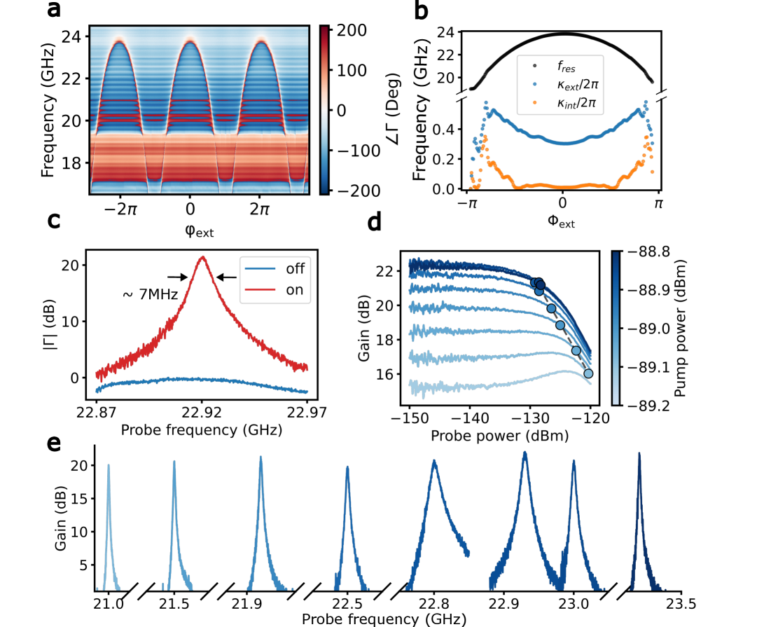
We first characterized the broadband linear response of the WJPA in a dilution refrigerator operated below 20 mK using a vector network analyzer (VNA). As shown in Fig. 2(a), the resonance from the lumped-element nonlinear resonator was observed to be periodic with external flux, as expected. We identified a parasitic mode near 19.5 GHz with a linewidth of approximately 500 MHz whose position shifted across thermal cycles. We surmise that this mode originates from non-ideal sealing of the copper package. Additionally, we observed ripples in phase of about and in magnitude of about dB across the measured band (not shown), which we attribute to impedance mismatches at microwave interfaces between components in the setup. At each flux bias, the extracted resonant frequency and coupling rates are shown in Fig. 2(b). Near zero flux bias, the resonator remains overcoupled with minimal variation in the coupling rate, consistent with simulations discussed in the supplementary Sec. I. As the flux bias is increased, the resonator approaches critical coupling near 19.5 GHz, likely due to the parasitic mode.
Next, we evaluate the amplification performance of the WJPA by measuring its reflection gain. The device was tested as a single-pump four-wave mixing (4WM) amplifier with a single microwave pump tone applied slightly below the bare resonance frequency to activate parametric gain. An example, shown in Fig. 2(c), demonstrated reflection gain over 20 dB with approximately 7 MHz bandwidth.
To characterize the amplifier’s dynamic range, we measure gain compression as a function of input probe power for various fixed pump powers, as shown in Fig. 2(d). The 1 dB compression points (), marked with circles, is about -125 dBm at 20 dB of maximum gain. increases as the gain is decreased, and the extracted values decrease approximately linearly with pump power on a logarithmic scale, with a fitted slope of 0.6. This trend aligns with theoretical analysis and prior experimental observations where gain saturation arises from Kerr-induced detuning and pump depletion Eichler and Wallraff (2014); Planat et al. (2019).
Finally, by tuning the magnetic flux through the SQUID loop, the resonant frequency of the amplifier is continuously adjusted. As demonstrated in Fig. 2(e), the WJPA supports parametric gain exceeding 20 dB across a frequency range from 21 GHz to 23.5 GHz, with typical bandwidth of 3 MHz. This result highlights its suitability for aligning over a broad frequency range with a readout resonator coupled to a qubit.
IV WJPA noise characterization
Characterization of the added noise of a Josephson amplifier is crucial for its application in qubit readout. In this work, we implemented two methods to characterize the noise performance of the WJPA and cross checked the results. The experiment wiring configurations for both methods can be found in supplementary Sec. II. We start by using the Y-factor technique with a variable temperature source (VTS) Malnou et al. (2024), consisting of a 50 matched microwave attenuator thermally anchored to a copper bracket with a heater and ruthenium oxide thermometer, and thermally isolated from the mixing chamber stage of the dilution refrigerator. By varying the VTS temperature, thermal noise is generated corresponding to a known photon occupation number , where , are Planck and Boltzmann constants, is the frequency and is the attenuator temperature.
Fig. 3(a) shows the measured output noise power versus frequency for various . Unlike the expectation for an ideal linear amplifier where would increase with , we observe a reduction in output noise with increasing temperatures. As discussed in Ref. Malnou et al., 2024, this behavior arises because of gain compression, from the broadband Johnson noise at elevated saturating the amplifier and reducing its gain.
This gain compression is visualized in Fig. 3(b), where we plot the gain versus frequency measured by the VNA for each . The gain decreases with increasing , dropping from 21.6 dB at 0.1 K to 12.9 dB at 1.75 K. To correctly extract the added noise, we account for this gain reduction by scaling the noise spectrum with the measured gain following the procedure discussed in Ref. Malnou et al., 2024, and further described in supplementary Sec. III. The resulting JPA-added noise as a function of frequency is shown in Fig. 3(c). It shows that across the amplifier bandwidth, the WJPA added noise is approximately 2 photon.
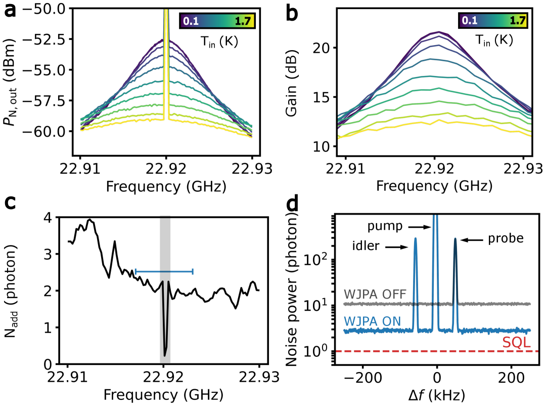
Next, we implemented a qubit-based noise calibration approach using a transmon-cavity system Macklin et al. (2015); Bultink et al. (2018) with a readout cavity frequency of GHz. Details of this method is described in supplementary Sec. IV. Fig. 3(d) shows the calibrated noise spectrum referenced to the input of the WJPA, acquired at 22 GHz. When the WJPA is turned off, the system noise is dominated by the HEMT, measured to be approximately 10.3 photons, or 10.9 K at 22 GHz. With the WJPA turned on, the total system added noise drops to photon, or K. Note that includes small contributions from the residual added-noise of the rest of the amplification chain after the WJPA. We can also express these results in terms of a measurement efficiency of with the WJPA turned on, compared to 9.7% with the WJPA turned off.
To summarize, both noise calibration methods indicate the system added noise with the WJPA operating of approximately 2 photon. This value is likely limited by losses in coaxial cables and circulators between the VTS/qubit measurement plane and the WJPA port, which could be improved with high-frequency microwave system engineering in the future. Overall, this noise performance confirms the WJPA’s capability to operate near the quantum limit and substantially improve fidelity of measurement in high-frequency readout applications.
V Conclusion
In summary, we have demonstrated a wireless, waveguide-coupled Josephson parametric amplifier (WJPA) that features a lumped-element resonator embedded with a JJ SQUID and coupled to the input/output port via a lithographically defined waveguide-to-slotline coupling structure. Operated in four-wave mixing mode with a single pump tone, the WJPA achieves over 20 dB of gain across a tunable range from 21 GHz to 23.5 GHz, with typical 3 MHz bandwidth. Using both Y-factor measurements and a qubit-based noise calibration, we extract an system added noise of approximately two photons. These results represent the first demonstration of a Josephson parametric amplifier operating above 20 GHz.
While this work realized a WJPA with Al/AlOx junctions, the design is readily implementable with Josephson elements realized with superconductors such as niobium, that can operate at high temperature KAnferov et al. (2025). Thus, this amplifier design is suitable for high-fidelity, fast qubit readout in high-temperature superconducting qubit systems.
Acknowledgment
This work was supported by the Defense Advanced Research Projects Agency (Grant No. HR00112420343), the Army Research Office (Grant No. W911NF-23-1-0251 and W911NF-23-1-0096) and the Air Force Office of Scientific Research (Grant No. FA9550-22-1-0203). HMC was supported in part by an appointment to the Department of Defense (DOD) Research Participation Program administered by the Oak Ridge Institute for Science and Education (ORISE) through an interagency agreement between the U.S. Department of Energy (DOE) and the DOD. ORISE is managed by Oak Ridge Associated Universities (ORAU) under DOE contract number DE-SC0014664. Sample fabrication was performed in the University of Texas at Austin Microelectronics Research Center, a member of the National Nanotechnology Coordinated Infrastructure (NNCI), which is supported by the National Science Foundation (Grant No. ECCS-2025227). All opinions expressed in this paper are the author’s and do not necessarily reflect the policies and views of DOD, DOE, or ORAU/ORISE.
DATA AVAILABILITY
The data that support the findings of this study are openly available on Zenodo at doi.org/10.5281/zenodo.15657612.
References
- Google Quantum AI and Collaborators (2025) Google Quantum AI and Collaborators, “Quantum error correction below the surface code threshold,” Nature 638, 920–926 (2025).
- Gao et al. (2025) D. Gao, D. Fan, J.-W. Pan, and et al., “Establishing a new benchmark in quantum computational advantage with 105-qubit zuchongzhi 3.0 processor,” Phys. Rev. Lett. 134, 090601 (2025).
- Magnard et al. (2018) P. Magnard, P. Kurpiers, B. Royer, T. Walter, J.-C. Besse, S. Gasparinetti, M. Pechal, J. Heinsoo, S. Storz, A. Blais, and A. Wallraff, “Fast and unconditional all-microwave reset of a superconducting qubit,” Phys. Rev. Lett. 121, 060502 (2018).
- Johnson et al. (2012) J. E. Johnson, C. Macklin, D. H. Slichter, R. Vijay, E. B. Weingarten, J. Clarke, and I. Siddiqi, “Heralded state preparation in a superconducting qubit,” Phys. Rev. Lett. 109, 050506 (2012).
- Krantz et al. (2019) P. Krantz, M. Kjaergaard, F. Yan, T. P. Orlando, S. Gustavsson, and W. D. Oliver, “A quantum engineer’s guide to superconducting qubits,” Applied Physics Reviews 6, 021318 (2019).
- Anferov et al. (2024a) A. Anferov, S. P. Harvey, F. Wan, J. Simon, and D. I. Schuster, “Superconducting qubits above 20 ghz operating over 200 mk,” PRX Quantum 5, 030347 (2024a).
- Anferov et al. (2025) A. Anferov, F. Wan, S. P. Harvey, J. Simon, and D. I. Schuster, “Millimeter-wave superconducting qubit,” PRX Quantum 6, 020336 (2025).
- Purmessur et al. (2025) C. Purmessur, K. Chow, B. van Heck, and A. Kou, “Operation of a high-frequency, phase-slip qubit,” (2025), arXiv:2502.07043 [cond-mat.supr-con] .
- Swiadek et al. (2024) F. m. c. Swiadek, R. Shillito, P. Magnard, A. Remm, C. Hellings, N. Lacroix, Q. Ficheux, D. C. Zanuz, G. J. Norris, A. Blais, S. Krinner, and A. Wallraff, “Enhancing dispersive readout of superconducting qubits through dynamic control of the dispersive shift: Experiment and theory,” PRX Quantum 5, 040326 (2024).
- Nesterov and Pechenezhskiy (2024) K. N. Nesterov and I. V. Pechenezhskiy, “Measurement-induced state transitions in dispersive qubit-readout schemes,” Phys. Rev. Appl. 22, 064038 (2024).
- Kurilovich et al. (2025) P. D. Kurilovich, T. Connolly, C. G. L. Bøttcher, D. K. Weiss, S. Hazra, V. R. Joshi, A. Z. Ding, H. Nho, S. Diamond, V. D. Kurilovich, W. Dai, V. Fatemi, L. Frunzio, L. I. Glazman, and M. H. Devoret, “High-frequency readout free from transmon multi-excitation resonances,” (2025), arXiv:2501.09161 [quant-ph] .
- Aumentado (2020) J. Aumentado, “Superconducting parametric amplifiers: The state of the art in josephson parametric amplifiers,” IEEE Microwave Magazine 21, 45–59 (2020).
- Roy and Devoret (2016) A. Roy and M. Devoret, “Introduction to parametric amplification of quantum signals with josephson circuits,” Comptes Rendus Physique 17, 740–755 (2016), quantum microwaves / Micro-ondes quantiques.
- Narla et al. (2014) A. Narla, K. M. Sliwa, M. Hatridge, S. Shankar, L. Frunzio, R. J. Schoelkopf, and M. H. Devoret, “Wireless josephson amplifier,” Applied Physics Letters 104, 232605 (2014).
- Anferov et al. (2024b) A. Anferov, S. P. Harvey, F. Wan, K.-H. Lee, J. Simon, and D. I. Schuster, “Low-loss millimeter-wave resonators with an improved coupling structure,” Superconductor Science and Technology 37, 035013 (2024b).
- Manucharyan et al. (2007) V. E. Manucharyan, E. Boaknin, M. Metcalfe, R. Vijay, I. Siddiqi, and M. Devoret, “Microwave bifurcation of a josephson junction: Embedding-circuit requirements,” Phys. Rev. B 76, 014524 (2007).
- Nigg et al. (2012) S. E. Nigg, H. Paik, B. Vlastakis, G. Kirchmair, S. Shankar, L. Frunzio, M. H. Devoret, R. J. Schoelkopf, and S. M. Girvin, “Black-box superconducting circuit quantization,” Phys. Rev. Lett. 108, 240502 (2012).
- Frattini et al. (2018) N. E. Frattini, V. V. Sivak, A. Lingenfelter, S. Shankar, and M. H. Devoret, “Optimizing the nonlinearity and dissipation of a snail parametric amplifier for dynamic range,” Phys. Rev. Appl. 10, 054020 (2018).
- Schackert (2013) F. D. O. Schackert, A Practical Quantum-Limited Parametric Amplifier Based on the Josephson Ring Modulator, Ph.d. dissertation, Yale University (2013).
- Eichler and Wallraff (2014) C. Eichler and A. Wallraff, “Controlling the dynamic range of a josephson parametric amplifier,” EPJ Quantum Technology 1, 2 (2014).
- Planat et al. (2019) L. Planat, R. Dassonneville, J. P. Martínez, F. Foroughi, O. Buisson, W. Hasch-Guichard, C. Naud, R. Vijay, K. Murch, and N. Roch, “Understanding the saturation power of josephson parametric amplifiers made from squid arrays,” Phys. Rev. Appl. 11, 034014 (2019).
- Malnou et al. (2024) M. Malnou, T. F. Q. Larson, J. D. Teufel, F. Lecocq, and J. Aumentado, “Low-noise cryogenic microwave amplifier characterization with a calibrated noise source,” Review of Scientific Instruments 95, 034703 (2024).
- Macklin et al. (2015) C. Macklin, K. O’Brien, D. Hover, M. E. Schwartz, V. Bolkhovsky, X. Zhang, W. D. Oliver, and I. Siddiqi, “A near–quantum-limited josephson traveling-wave parametric amplifier,” Science 350, 307–310 (2015).
- Bultink et al. (2018) C. C. Bultink, B. Tarasinski, N. Haandbæk, S. Poletto, N. Haider, D. J. Michalak, A. Bruno, and L. DiCarlo, “General method for extracting the quantum efficiency of dispersive qubit readout in circuit qed,” Applied Physics Letters 112, 092601 (2018).