In-Memory Non-Binary LDPC Decoding
Abstract
Low-density parity-check (LDPC) codes are an important feature of several communication and storage applications, offering a flexible and effective method for error correction. These codes are computationally complex and require the exploitation of parallel processing to meet real-time constraints. As advancements in arithmetic and logic unit technology allowed for higher performance of computing systems, memory technology has not kept the same pace of development, creating a data movement bottleneck and affecting parallel processing systems more dramatically. To alleviate the severity of this bottleneck, several solutions have been proposed, namely the processing in-memory (PiM) paradigm that involves the design of compute units to where (or near) the data is stored, utilizing thousands of low-complexity processing units to perform out bit-wise and simple arithmetic operations. This paper presents a novel efficient solution for near-memory non-binary LDPC decoders in the UPMEM system, for the best of our knowledge the first real hardware PiM-based non-binary LDPC decoder that is benchmarked against low-power GPU parallel solutions highly optimized for throughput performance. PiM-based non-binary LDPC decoders can achieve Mbit/s of decoding throughput, which is even competitive when compared against implementations running in edge GPUs.
Keywords LDPC Codes Non-binary LDPC Decoding Parallel Signal Processing Processing in-Memory UPMEM.
1 Introduction
Low-density parity-check codes are important components in the communications [1, 2, 3, 4], and data storage [5, 6] fields. The strong error-correcting capability of low-density parity-check codes allows them to approach the Shannon limit [7], and, more recently, they have been adopted in the G New Radio technical specification [8, 9]. Nevertheless, developing efficient low-density parity-check decoders presents significant challenges due to their demanding computational requirements and memory access patterns. Over the years, researchers have proposed parallel approaches on different hardware platforms, including central processing units [10, 11], graphics processing units [12, 13], field-programmable gate arrays [14, 15] , and application-specific integrated-circuits [16, 17] to improve throughput performance and meet latency constraints. However, the partial-parallel nature of these decoders still faces challenges in the computations of the partial results, which, in turn, increases data transfers between computational units and memory.
Low-density parity-check codes were proposed in by Robert Gallager [18] but were considered impractical due to their computational complexity. In , Davey and MacKay proposed the non-binary low-density parity-check codes as an extension to the binary low-density parity-check codes that allowed to achieve better error-correction performance for moderate code lengths at the cost of higher computational complexity [7, 19]. In the last two decades, the development of more efficient computational systems allowed the implementation of low-density parity-check decoders in error correction applications using parallel computing architectures such as central processing units, graphics processing units, field-programmable gate arrays, and application-specific integrated-circuits. These platforms allowed decoders to increase their throughput performance. However, when choosing a platform to compute such a highly complex subclass of low-density parity-check codes, a trade-off between throughput, latency, memory accesses, energy consumption, error-correction capability, flexibility, and cost must be made [16, 20].
Over the past few decades, the development of computing units has adhered to Moore’s law, where the transistor count doubles approximately every months for the same area. However, challenges in dynamic random-access memory scaling (increasing density and performance while maintaining reliability, latency, and energy consumption) have caused memory technology to not match the same pace of development as computational units, thus leading to a "data movement bottleneck" [21, 22]. This bottleneck is present in most modern computing systems. It happens when a significant part of the execution time is spent on data transfers between memory and processing units.
These obstacles in improving dynamic random-access memory technology have motivated the industry and researchers to rethink and redesign memory systems [23], such as D stacked [24] and non-volatile memories [25]. Several new approaches propose a paradigm shift from a processor-centric design to a processing-in-memory design [26] where the memory units are designed to incorporate computational capability, allowing to alleviate the "data movement bottleneck" by computing data where (or near) it resides [22, 26, 25].
Currently, processing-in-memory systems can be divided into two main areas:
-
•
Processing-near-memory incorporates computing units near the memory, such as D stacked memory, which integrates several memory layers with one (or more) logic layer(s) [27]. Processing-near-memory supports a large range of operations. However, the main downside is that these systems suffer from area and thermal constraints, have limited capacity, and have a high cost [27].
-
•
Processing-using-memory takes advantage of the analog circuit properties of memory cells (static random-access memory [28], dynamic random-access memory [29], and non-volatile memories [30]) to perform simple bitwise operations (AND and OR operations) [31]. Although very efficient in terms of performance, the drawback is that this paradigm requires a major reorganization of memory circuitry to enable more complex operations to be performed [31].
Due to the challenges mentioned above, the industry is still designing computing systems with processing-in-memory technology. The UPMEM processing-in-memory architecture is the first commercial realization of a processing-near-memory system implemented in hardware [32, 27]. This system is a massive multicore-central processing unit with private memory that takes advantage of the more mature fabrication and design of D dynamic random-access memory to incorporate computational units in the same chip [32, 27], allowing the implementation of several independent DRAM processing unit cores with deep pipelines ( stages) and fine-grained multithreading (up to threads) [32].
To address the performance bottlenecks associated with data transfers in LDPC decoding, this paper proposes the implementation of low-density parity-check decoders in processing-near-memory architectures. Integrating low-density parity-check decoding into processing-in-memory can significantly alleviate the data movement bottleneck between memory and compute units, thereby enhancing overall performance. In the UPMEM system, we leverage the advantages of the memory hierarchy (main DRAM, working SRAM) to minimize data transfers, particularly in scenarios where irregular memory access patterns pose significant challenges. We also take advantage of multithreading and -bit multipliers supported by the simple arithmetic logic unit across several DRAM processing units to maximize throughput performance. By exploiting processing-near-memory architectures, this paper aims to demonstrate how leveraging processing-in-memory technology can effectively mitigate the performance limitations encountered in typical parallel low-density parity-check decoding implementations, ultimately enabling substantial improvements in real-time processing capabilities.
While non-binary low-density parity-check decoders have been extensively explored on central processing units, graphics processing units, and field-programmable gate arrays [16], their implementation on processing-in-memory architectures remains largely unexplored. Therefore, this paper proposes the following contributions:
-
•
The first processing-in-memory-based non-binary low-density parity-check Fast Fourier transform-Sum-product algorithm and Min-max decoder implementations, to the best of our knowledge.
-
•
An efficient mapping of the non-binary low-density parity-check decoders to the UPMEM architecture, exploiting the system’s memory hierarchy (main DRAM, working SRAM), multithreading, multicodeword decoding, and -bit multipliers, in order to avoid the UPMEM’s processing limitations for floating-point operations.
-
•
Performance comparison against low-power parallel architectures, such as embedded graphics processing units, using real codes recommended by the Consultative Committee for Space Data Systems- [33].
2 Belief Propagation
Belief propagation is an iterative message-passing algorithm used in graphical models to infer properties of a small data set from the observation of a larger data set. This algorithm is successfully applied in information theory, artificial intelligence, computer vision, and decision support systems, with the principal applications of belief propagation being low-density parity-check codes [18], turbo codes [34], and Bayesian networks [35].
Graphs are structures that represent relationships between objects (also called nodes). The belief propagation algorithm calculates the probability distribution of a subset of nodes. The information gathered from calculated distributions can be used to infer the properties of objects from other subsets that maintain relationships between them. For instance, a belief network is used in a medical diagnosis support system to establish relationships between symptoms and diseases [36] or in image classification [37], as depicted in Fig. 1.
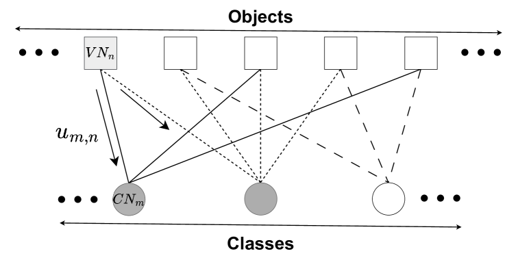
In the case of low-density parity-check codes, a bipartite graph describes the mathematical relationships between several nodes, where probabilities are exchanged between them.
2.1 Non-binary LDPC Codes
Noise is an inherent and undesirable part of most communication systems. In digital data communications, data is transmitted from the source to a receiver through a channel. However, the channel is susceptible to noise that corrupts and changes bits during transmission, requiring the deployment of error correcting codes (for instance, low-density parity-check codes) in the receiver to detect and correct the erroneous bits. This provides resilience to noise in data.
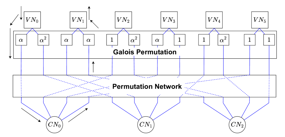
An non-binary low-density parity-check code is a linear block code defined by the sparse parity-check matrix of size by , in or a Tanner graph representation, as illustrated in Fig. 1 and 2 [38]. represents the number of rows of or the number of check nodes in the Tanner graph, while indicates the number of columns or the number of variable nodes. For instance, in (1), rows or three check nodes and columns or six variable nodes. The connection between check nodes and variable nodes is established by the non-zero elements of , in (1), the is connected to , and the is not connected to . An low-density parity-check code is considered regular when each row contains the same number of non-zero elements (check node degree), and each column also contains an equal number of non-null elements (variable node degree). Conversely, if the check node degree () and the variable node degree () varies, the code is considered irregular. Irregular codes offer improved coding performance but require higher computational complexity.
Barnault and Declercq proposed non-binary low-density parity-check that can be decoded using Galois fields up to [39]. A Galois field is a mathematical field with finite elements, represented as , where indicates the field’s cardinality [39] (). Galois fields are constructed under a specific set of properties, ensuring that any operation performed over a Galois field returns a result within the same field. In computational terms, operations in Galois fields allow the simplification of arithmetic logic units since circuits are no longer required for carry flags and integer overflow [40].
Irreducible primitive polynomials define a -order Galois field. Non-binary low-density parity-check codes use the finite field in , where the elements are represented as , with being a primitive element of [38].
The non-binary low-density parity-check code presented in (1), has the primitive polynomial . non-binary low-density parity-check codes compute symbols in their respective Galois field, with each symbol representing bits. For the example provided in Fig. 2 (), each symbol represents two bits.
| (1) |
Formally, a non-binary low-density parity-check code size is denoted as , where . During transmission, a codeword can be corrupted by noise. At the receiver, the non-binary decoder should receive a codeword with symbols that will be corrected, if necessary.
2.2 Non-binary LDPC Decoding Algorithms
In non-binary low-density parity-check codes, instead of using single bits (), the messages are encoded into symbols composed of -tuples of bits (e.g. ) to correct transmission errors over the channel.
The first step is to compute the probability vector using the data received from the channel for every symbol in (). Assuming binary phase-shift keying modulation, an additive white Gaussian noise channel, and that the received bits are independent, the probability of a received symbol can be calculated through the product of the independent bit. For instance, if the probability of a received bit being is and being is , the probability of a symbol being ’’ in is . Generalizing for additive white Gaussian noise, the probability for each symbol can be calculated through and , where the probabilities of the symbols are proportional to the productory, since it requires them to be normalized to guarantee the axioms () [38].
Input: ; , ,
Initialization:
for
Compute ; Stop if
Permutation
For each variable node , each , each
| (2) |
Check node processing (CNP)
For each check node , each , each
| (3) |
Depermutation
For each check node , each , each
| (4) |
Variable node processing (VNP)
For each variable node , each , each
| (5) |
| (6) |
A posteriori information computation & Hard decision
For each variable node , each
The non-binary low-density parity-check decoding algorithm tries to seek a codeword such that maximizes , meaning that is calculated through an iterative process until satisfying all parity check equations or until a maximum number of iterations () is reached. This can be achieved by calculating the maximum a posteriori probability of every variable node and check node. However, the calculation of the a posteriori probabilitys of every node is computationally expensive and can be simplified by excluding the information of unconnected nodes and considering the set of connected nodes except one node ( with ). The node should cycle through the set , allowing the algorithm to calculate the most probable symbols for the decoded codeword .
In summary, the non-binary low-density parity-check decoders exchange messages between check nodes and variable nodes, where these messages are vectors containing the probability of each symbol being correct that update when exchanged between nodes
Davey and MacKay proposed the non-binary formulation of the sum-product algorithm [7], but it has high computational complexity. One solution to decrease complexity in the check node processing is to avoid the convolution of probabilities and compute them in the frequency domain, as depicted in Algorithm 1.
Input: ; , ,
Initialization:
For
Compute ; Stop if
Check node processing (CNP), F & B matrices
For each check node , each , each
If
| (7) |
| (8) |
Else
For each
| (9) |
| (10) |
Check node processing (CNP), matrix
For each check node , each , each
If
| (11) |
Else if
| (12) |
Else
For each
| (13) |
Variable node processing (VNP)
For each variable node , each , each
| (14) |
| (15) |
A posteriori information computation & Hard decision
For each variable node , each
The fast Fourier transform-sum-product algorithm reduces the complexity of the check node processing. However, it requires floating-point (or quantization schemes) and division operators. The decoder complexity can be further reduced by computing the probabilities in the logarithmic domain with respect to the most probable symbol. Savin [41] proposed the min-max described in Algorithm 2, showing that by using appropriate metrics, the number of complex operations can be reduced, producing a quasi-optimal decoder.
Furthermore, the messages exchanged in the fast Fourier transform-sum-product algorithm must be multiplied by when exchanged from check nodes to variable nodes and divided when exchanged from variable nodes to check nodes in their respective Galois fields. For example, the probabilities are multiplied as follows:
This operation can be performed by executing a barrel shift where the first element is fixed. For instance, the message propagated from to in Fig. 2, will be multiplied by . Some decoding algorithms (such as the min-max), feature additions in Galois field that can be simplified to an XOR operation.
|
Multiplications | Divisions | Comparisons | Memory Transactions | |||||
| FFT-SPA |
|
||||||||
| Permutation | |||||||||
|
|||||||||
| fast Fourier transform | |||||||||
| check node processing Productory | |||||||||
| Inverse fast Fourier transform | |||||||||
|
|||||||||
| Depermutation | |||||||||
|
|||||||||
| VNP | |||||||||
| Min-Max |
|
||||||||
|
|||||||||
|
|||||||||
|
|||||||||
|
|||||||||
|
|||||||||
|
|||||||||
|
|||||||||
|
|||||||||
| VNP | |||||||||
The min-max decoding algorithm computes the log-likelihood ratio vectors with respect to the most likely symbol (), resulting in a vector with elements. The most likely symbol of the field can calculated through .
The main difference lies in the check node processings, which replace sums and products by comparisons, using a forward and backward computation technique [41]. Furthermore, using log-likelihood ratios instead of the most likely symbol, reduces the number of comparisons between symbols in the same message, reducing computational complexity.
2.3 Theoretical Decoding Complexity
The number of operations and memory transactions of each decoding algorithm are presented in Table 1. Additions/subtractions in Galois fields are equivalent to XOR operations and multiplications/divisions in Galois fields are equivalent to read and write operations (barrel shift operations). In order to improve performance, these operations are implemented in look-up tables.
The fast Fourier transform-sum-product algorithm uses a high number of additions and multiplications in the check node processing (complexity of ) and variable node processing (complexity of ), where the check node processing complexity dominates the the complexity of the fast Fourier transform-sum-product algorithm, as compared to the variable node processing. The overall expression representing the total number of operations (excluding memory transactions) is .
In terms of memory transactions, the complexity is mostly located in the fast Fourier transform, inverse fast Fourier transform, and variable node processing. The memory transaction complexity in the check node processing is and for the variable node processing is , where the overall complexity is the same as the complexity of the check node processing (). The total number of memory transactions in the fast Fourier transform-sum-product algorithm is described by .
In comparison to the fast Fourier transform-sum-product algorithm, the min-max algorithm transforms multiplications and divisions into additions/subtractions and comparisons, with most operations located in the Forward and Backward, and matrices computation. The check node processing has a computational complexity of , while the variable node processing has a complexity of , with an overall computational complexity . The general expression describing the total number of operations in min-max without memory transactions is .
The Forward and Backward, and matrices have the highest number of memory transactions in the min-max. The memory transaction complexity is the same as the computational complexity, with the expression representing the total number of memory transactions in the min-max.
The theoretical computational and memory transaction complexity mainly scales with the size of Galois field, since is usually lower than [16]. At first glance, processing-in-memory solutions might not seem attractive to implement low-density parity-check decoders due to their limited clock speed and arithmetic logic units compared to other devices. However, by using reduced precision formats and several thousands of decoders in parallel, processing-in-memory systems can counteract the downsides of having lower clock frequencies.
3 UPMEM System
Parallel processing platforms, such as graphics processing units, field-programmable gate arrays, and application-specific integrated-circuits, can offload specific tasks from the central processing unit to further enhance computational capabilities by allowing multiple processes to run simultaneously. These platforms leverage concurrency to solve problems more quickly, either by dividing tasks into smaller subtasks that can be processed in parallel or by executing different tasks in parallel to increase throughput.
Programming models for central processing units, graphics processing units, field-programmable gate arrays, and application-specific integrated-circuits differ significantly due to their distinct architectures and intended applications. For example, central processing units use programming models optimized for task scheduling and execution on operating systems. On the other hand, graphics processing units are designed for massive parallelism, using thousands of lightweight threads that execute the same instructions on different data.
The UPMEM system is a massive multicore-central processing unit with private memory that employs several simple on-chip computing units using a reduced instruction set computer-based instruction set architecture. Using memory and processing units on the same chip imposes challenges in manufacturing design. For instance, memory technology is optimized for density (more memory cells per unit of area or volume), and processor technology is optimized for speed. Combining the two technologies causes thermal dissipation problems, causing the processing unit’s clock frequency to be reduced, the reduction of memory density, and the employment of active cooling strategies to increase the system’s complexity with limited effectiveness (memory technology still needs low temperatures to operate).
UPMEM addresses these problems by implementing near-memory processing units, called DRAM processing units (DPUs), with relatively deep pipelines and fine-grained multithreading running at several hundred megahertz.
3.1 UPMEM Architecture
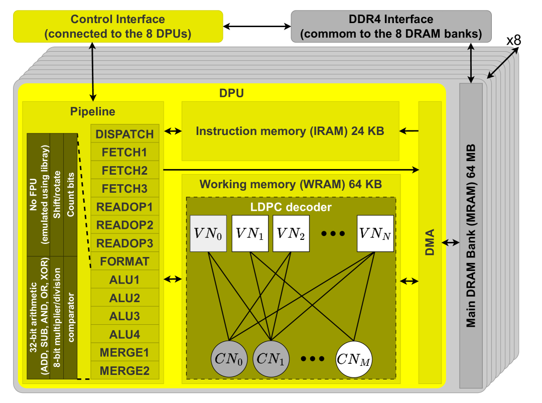
A general overview of the UPMEM system is shown in Fig. 3, and the internal architecture of a single DRAM processing unit is detailed in Fig. 4. A DRAM processing unit is a -bit reduced instruction set computer-based unit that operates in-order and supports multithreading with a proprietary instruction set architecture [42]. Each DRAM processing unit supports up to hardware threads, each with 2-bit registers. As depicted in Fig. 4, DRAM processing unit has a -stage pipeline. However, only the last three stages (ALU4, MERGE1, and MERGE2) are executed in parallel with the DISPATCH and FETCH stages within the same thread. Therefore, instructions from the same thread are dispatched in -cycle intervals, which requires only threads to fully exploit the pipeline [27, 42].
The DRAM processing unit arithmetic logic unit supports -bit additions/subtractions and bitwise operations, shift/rotate operations, bit counters, and -bit multiplications/divisions. -bit multiplications and divisions are not natively supported due to the high hardware cost and the limited number of metal layers [42], but are emulated by using -bit multiplications/divisions and shift operations. Furthermore, the DRAM processing unit does not have floating-point functional units and emulates floating-point operations using software libraries ( cycles for a x floating-point multiplication).
The hardware threads use a shared instruction memory (instruction DRAM) and a scratchpad memory (working SRAM). The KB instruction DRAM supports up to -bit encoded instructions. The faster static random-access memory-based working SRAM has a size of KB and can be accessed through , , , and -bit load/store operations. The DRAM processing units also include a slower MB dynamic random-access memory-based main DRAM, which uses direct memory access instructions to transfer data from the main DRAM bank to the instruction DRAM and working SRAM.
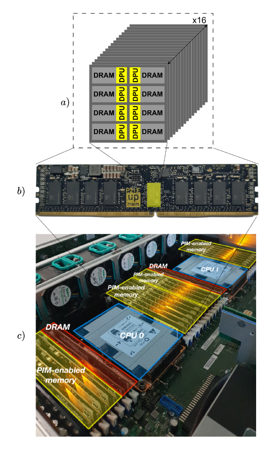
Each UPMEM processing-in-memory chip is composed of eight DRAM processing units with a control and a double data rate 4 interfaces. Each UPMEM module comprises processing-in-memory chips, as shown in Fig. 3. The UPMEM server includes two central processing units, conventional dynamic random-access memory modules, and processing-in-memory modules, as shown in Fig. 3 containing a total of DRAM processing units and GB of main DRAM running at MHz.
3.2 UPMEM Programming Model
The UPMEM follows a single program, multiple data programming model, where the same binary is loaded in each DRAM processing unit, and threads execute the same code on separate data fragments. The UPMEM software development kit includes a C LLVM-based compiler, debugger, and runtime and host libraries, allowing the DRAM processing unit programs to be written in the C language and the host program to be written in C, C++, Python, or Java [43].
The host central processing unit compiles both host and device code. The programmer is responsible for allocating the number of DRAM processing units and threads, defining the data to be transferred between the host and the device, and setting the synchronous/asynchronous kernel execution mode. Synchronous execution stops the central processing unit thread until all DRAM processing units have finished executing the kernel, while asynchronous execution immediately grants control back to the host central processing unit.
Parallel data transfers from central processing unit to DRAM processing unit can be performed using three different functions: dpu_copy_to() copies data to a single-DRAM processing unit. dpu_push_xfer() copies different chunks of data from a single buffer to a set of DRAM processing units. dpu_broadcast_to() copies data from a single buffer to several DRAM processing units within the same set. Two functions can be used to retrieve data from DRAM processing units: dpu_copy_from() copies data from a single-DRAM processing unit to the host buffer. dpu_push_xfer() copies data from several DRAM processing units to a single host buffer (the function dpu_push_xfer() can copy data from or to DRAM processing units by setting a function’s argument). The transfer sizes are the same, using dpu_push_xfer() and dpu_broadcast_to() functions results in parallel transfers and increases bandwidth.
Data transfers between main DRAM and working SRAM do not have cache mechanisms, which the programmer must explicitly manage by using mram_read() (main DRAM to working SRAM transfers) and mram_write() (working SRAM to main DRAM transfers).
The UPMEM runtime library contains thread control and synchronization mechanisms, such as mutexes that define critical sections between threads, semaphore counters, barriers that synchronize several threads at a specific point in the code, and handshakes that enable synchronization between pairs of threads.
3.3 Comparison to GPU Architecture
From a high-level perspective, the UPMEM system shares some similarities with graphics processing units. However, their architectures and hierarchies are fundamentally different.
The biggest difference lies in the memory hierarchy. Graphics processing units have a main dynamic random-access memory, which is accessible by all threads in the graphics processing unit, and a faster static random-access memory shared memory, which is accessible by threads in the same streaming processor. UPMEM also has dynamic random-access memory and static random-access memory but they are accessible by threads within the same DRAM processing unit. This configuration increases data synchronization costs in the UPMEM system since data transmitted between DRAM processing units travels through the memory bus.
The second difference is that DRAM processing units have a simple in-order scalar arithmetic logic unit with no stall signals and instruction pipelining, allowing them to perform different stages of different threads in the same clock cycle. In contrast, graphics processing units have several vector arithmetic logic units grouped in a streaming multiprocessor. This allows them to perform operations at different data points in the same clock cycle with several dedicated single instruction, multiple data lanes. Furthermore, graphics processing units have schedulers that enable simultaneous multithreading by dynamically issuing instructions to maximize performance.
Both systems use an single program, multiple data programming model, where the same program is loaded into different processing units (into DRAM processing units in UPMEM, into streaming multiprocessors in graphics processing units). However, the execution model of graphics processing units is different than UPMEM. graphics processing units have a single instruction, multiple thread execution model with several independent single instruction, multiple data functional units, sharing dynamic random-access memory, static random-access memory, and cache between elements in the same streaming multiprocessor, while the UPMEM system has several scalar arithmetic logic units with interleaved pipelining, that have DRAM processing unit-visible dynamic random-access memory and static random-access memory without caching techniques.
4 Near-memory LDPC Parallel Implementation
This work selects two widely used non-binary low-density parity-check decoding algorithms: the fast Fourier transform-sum-product algorithm decoder and the min-max decoder. The fast Fourier transform-sum-product algorithm is used to evaluate the decoder performance when using floating-point arithmetic, serving as a performance reference. The min-max decoder, on the other hand, is implemented using fixed-point arithmetic to explore the low-complexity, quantized decoding regime. This combination allows to assess the trade-offs between floating-point emulation and native integer operations on the UPMEM platform.
The proposed parallelization methods for low-density parity-check decoders employ an single program, multiple data model for several simple processing cores. The implementations for binary low-density parity-check decoders in graphics processing unit and the UPMEM system have been published in [44, 45].
While this work follows the same multicodeword mapping strategy used in prior binary low-density parity-check implementations on UPMEM [44, 45], the implementation of non-binary low-density parity-check decoders introduces significant differences. Non-binary low-density parity-check decoding involves operations over Galois fields, which require more complex arithmetic (finite field multiplication, fast Fourier transform-based convolutions, log-likelihood ratio updates) and larger message representations. As a result, the memory footprint and computational requirements are substantially higher compared to binary low-density parity-check decoding. To accommodate these demands, the working SRAM usage must be optimized carefully, and additional synchronization points are required in multithreaded implementations. Furthermore, the non-binary low-density parity-check decoding process includes additional permutation and depermutation steps that are not present in binary decoding.
Two approaches can be taken to implement the low-density parity-check decoders. The first multicodeword approach assumes weak scaling by assigning a decoder to each DRAM processing unit and increasing the number of decoders by rising the number of DRAM processing units selected, thus eliminating the need for inter-DRAM processing unit synchronization. The second approach partitions the workload over several DRAM processing units, with the cost of inter-DRAM processing unit overhead increasing with the number of used DRAM processing units and the code characteristics (number of nodes, edges, iterations). In order to eliminate data communication overheads between DRAM processing units and increase performance (assuming the same number of codewords in both strategies), the first approach is chosen for this work, analyzing single-thread single-DRAM processing unit and multithread-multiple-DRAM processing units performances.
The multithreaded approach distributes the load over more than threads to fully utilize the DRAM processing unit pipeline. The non-binary low-density parity-check codes used in this work have sizes that are powers of two. Therefore, threads were used since it is the first power of two bigger than (please revisit section 3.1 for an explanation on the threads choice).
Although high levels of decoder replication are often used to maximize throughput in conventional parallel architectures, in the UPMEM system, each DRAM processing unit executes independently and asynchronously. This allows decoding tasks to begin as soon as codewords become available, without requiring synchronization or batching. While there may be an initial latency overhead due to setup and data transfer, this cost is quickly amortized as more codewords are decoded in parallel. Therefore, the proposed multicodeword solution not only enables high throughput but also maintains low per-codeword latency, making it suitable for real-time and low-latency communication scenarios involving short non-binary low-density parity-check codewords.
4.1 Optimization Techniques
Several optimization techniques can be implemented to enhance the performance of low-density parity-check decoders by exploiting the UPMEM system. These techniques maximize parallelism, minimize communication overheads, and efficiently utilize computational resources.
Working SRAM usage: working SRAM should be preferred over main DRAM by storing the Tanner graph characteristics as depicted in Fig. 4. An main DRAM/working SRAM read and write takes between and cycles (depending on the data transfer size) and can achieve a bandwidth of MB/s [27]. On the other hand, -byte loads and stores in working SRAM only take one clock cycle when the pipeline is full and can achieve a bandwidth of MB/s [27].
In our implementation, the partitioning between main DRAM and working SRAM is manually managed by the programmer, as the UPMEM software development kit does not provide mechanisms for automatic detection of data reuse or dynamic memory placement. All decoder buffers are allocated in working SRAM for fields up to , which allows faster access and higher throughput. For and , the working SRAM capacity is insufficient to store all required buffers, and less frequently accessed data, such as auxiliary buffers used in the fast Fourier transform or matrix computation, is explicitly offloaded to main DRAM.
Quantization: Low-density parity-check decoders use an floating-point representation to calculate the probabilities or log-likelihood ratios of bits in . However, using floating-point arithmetic is impractical due to area, power, and complexity constraints, specifically in hardware implementations. A workaround for these constraints is to use quantization schemes and integer or fixed-point arithmetic, resulting in decoders that are faster, less complex, more power efficient, and with a low memory footprint, at the cost of a small decrease in error-correction capability [46].
In the UPMEM system, the DRAM processing units do not feature floating-point arithmetic logic units, and these operations are instead emulated in software, taking between tens and thousands of cycles to perform. The maximum throughput of floating-point -bit arithmetic operations is MOPS for additions, MOPS for multiplications, and MOPS for divisions.
The DRAM processing units have a -bit integer arithmetic logic unit that can achieve MOPS for additions, MOPS for multiplications, and MOPS for divisions. Multiplications and divisions have lower throughput due to DRAM processing units having an -bit multiplier and emulating -bit multiplications/divisions using shifting operations, taking up to cycles. The -bit multiplier performs similarly to the -bit arithmetic logic unit when executing -bit arithmetic.
To take advantage of the hardware capability of DRAM processing units, quantization of the data received from the channel () is performed to the nearest integer. A clipping function is also used to ensure that the values are between and .
The effect of quantization on error-correction capability has been studied in the literature. In particular, Wymeersch et al. [47] show that using fixed-point quantization in non-binary log sum-product algorithm decoding results in minimal degradation in bit error rate performance. Their results indicate that quantization introduces a small performance loss, typically below dB without leading to visible error floors, even in high-signal-to-noise ratio regimes. This supports the use of quantization as a practical trade-off for performance in platforms with limited floating-point support such as UPMEM.
Loop unrolling: Loop unrolling removes branching operations from the arithmetic logic unit’s pipeline. Thus reducing the total number of operations at a cost of a higher memory footprint. The lack of automatic code optimization of the UPMEM toolchain requires the programmer to optimize the code manually. Loop unrolling is used in the fast Fourier transform and inverse fast Fourier transform operations of the fast Fourier transform-sum-product algorithm, leading to increased performance. However, for higher Galois fields, the unrolled code does not fit in instruction DRAM, and typical loops must be used.
4.2 FFT-SPA
The fast Fourier transform-sum-product algorithm described in Algorithm 1, uses six processing blocks: (2) represents the Permutation block, in (3) are represented the fast Fourier transform, check node processing productory, and inverse fast Fourier transform blocks, the depermutation in (4), and the variable node processing block is represented by (5) and (6). For the multithreaded implementation, in all blocks, the edges/messages ( or ) are processed by threads. Due to data dependencies, synchronization barriers are placed between each block to prevent data hazards.
| FFT-SPA | |
|---|---|
| Function | # of syncs. |
| Permutation | |
| FFT | |
| check node processing | |
| Inverse FFT | |
| Depermutation | |
| variable node processing | |
| Total | |
| Min-Max | |
|---|---|
| Function | # of syncs. |
| F & B Matrices | |
| Matrix | |
| VNP | |
| Total | |
The Permutation block (2) shifts the message using a Galois multiplication look-up table, saving the permutated messages in a temporary buffer to avoid read-after-write and with a synchronization barrier before the permutated messages are written back to memory.
The fast Fourier transform block employs a radix- implementation [48], which converts the convolution into the frequency domain, transforming the convolution operation into products. The outer loop of this block iterates between and , which is lower than . Using fewer than threads leads to an underutilization of the pipeline. Therefore, the chosen approach is to parallelize the inner loop (distribute the edges over threads) and place synchronization barriers at the end of each bit iteration. Furthermore, the inner loop has a synchronization barrier to remove read-after-write hazards, bringing the total number of synchronizations to in this block, as shown in Table 2.
Once in the frequency domain, all the configurations of the messages connected to the same check node are multiplied in the check node processing productory block.
Next, the inverse fast Fourier transform block is applied to the messages. This block applies the same operations as the fast Fourier transform. In addition, the normalization step in the fast Fourier transform block is transferred to this block, where the messages are divided by . The messages are then passed to the Depermutation block (4), which applies the same operations as the Permutation block.
In the variable node processing block (5), the same operations of the check node processing productory are performed, but instead to all configurations of messages connected to the variable nodes. The probability received from the channel is also considered in this operation. After the new messages are calculated and synchronized, they are normalized in (6) by the sum of all the probabilities in the same message (sum ) to grant the validity of the probabilites’ axioms.
4.3 Min-Max
The min-max implementation described in Algorithm 2 comprises two processing blocks: the first check node processing block is composed of the Forward (eq. (7) and (9)) and Backward (eq. (8) and (10)) matrices computation (F & B matrices) and the matrix computation (eq. (11), (12), and (13)). The second variable node processing block is composed of (14) and (15). The implementation follows the same data structure as the fast Fourier transform-sum-product algorithm, where the parallelism is exposed to the edges of the low-density parity-check code, and the synchronization barriers are placed at the end of each block, as described in Table 3.
The check node processing block permutates the symbols using the schemes described in Algorithm 2. The F & B matrices are computed based on the probabilities received from the variable nodes. The forward matrix (7) (9) is computed by comparing the probability from the previous edge and the probability of the received symbol from the connected variable node. The backward matrix (8) (10) is calculated in the same way, but instead of considering the probability from the previous edge, it uses the probability from the next edge. Therefore, the forward matrix is computed from the first to the last edge, and the backward matrix is computed from the last to the first edge. The computation (11) (11) (13) compares the permutated probabilities between the Backward matrix’s next edge and the Forward matrix’s previous edge.
The multithreaded approach exposes parallelism to inner loops and computes several fields in parallel. The limitation of this approach is that for smaller fields ( and ), it is only possible to use four or eight threads, resulting in a less efficient parallel code due to an under-utilization of the pipeline for lower fields.
The variable node processing block does not have the same issues as the check node processing block, and the edges/messages are distributed over threads. This block computes the sum of all configurations of messages ( matrix) connected to the same variable node and adds the sum to the probability received from the channel (14). To finalize, the newly calculated probabilities are subtracted by the lowest probability (15) to force the output of the check nodes to have the same log-likelihood ratio structure as defined in the initialization of the min-max [41, 49].
5 Experimental Results
The non-binary low-density parity-check codes used in this work are constructed from a non-binary code for from [1], resulting in three different non-binary low-density parity-check parity-check matrixs of sizes , , and with and for up to . For simplicity, the , , and codes are designated as , , and respectively.
The tests were performed on the UPMEM system and compared to low-power graphics processing units in the Jetsons Nano GB, TX, and AGX Xavier, as shown in Table 4. We developed all the parallel implementations proposed under the context of this work.
| UPMEM | Jetson Nano 2 GB | Jetson TX2 | Jetson AGX XAvier | |||||||||||
|
|
|
|
|
||||||||||
|
DPU 350 MHZ |
|
|
|
||||||||||
| Device cores | 2540 cores | 128 Cores | 256 Cores | 512 Cores | ||||||||||
| Device memory |
|
2 GB Shared with system | 8 GB Shared with system | 32 GB Shared with system | ||||||||||
| Storage memory |
|
|
|
|
||||||||||
| Power Modes | 23.22 W per dual in-line memory module | 10 W/ 5 W | 15 W/ 7.5 W | 30 W/ 10 W |
The experimental values achieved represent the average of runs. The graphics processing unit values were obtained by clock_time() using the MAX-N power mode. In the UPMEM system, the execution time was obtained through an internal cycle counter using perfcounter_config(COUNT_CYCLES, true), and the data transfer times between host and device were obtained using the UPMEM’s DRAM processing unit profiling tool, as recommended by the SDK manual [43].
These decoders do not assume early termination and the presented values exclude the processing of the parity check equation verifications (a posteriori information computation and hard decision processing blocks) in order to fix the number of decoding iterations. This design choice ensures a fair and objective comparison of throughput and decoding performance with other works in the literature, independently of channel conditions. Using early termination could bias the results by coupling decoder latency and throughput to the noise level, leading to less consistent performance metrics across different signal-to-noise ratio regimes. While early stopping can reduce average decoding time in practice, its omission here enables controlled benchmarking and avoids introducing conditional branches and thread synchronization overhead on the UPMEM architecture.
5.1 Decoding Complexity Validation
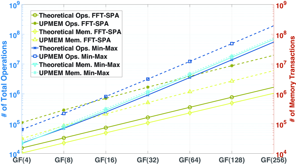
By choosing the low-density parity-check code, the theoretical computational complexity of the decoder can be derived for different fields. For the codes used in this work, the expressions of Table 1 can be computed and are depicted in Fig. 5 for the different decoding algorithms. Memory transactions are defined by data movement between memory and registers.
The fast Fourier transform-sum-product algorithm has a complexity of and it scales better for higher Galois fields, requiring an order of magnitude fewer operations (both arithmetic operations and memory transactions) for than the min-max algorithm, which has a complexity of . However, for and , the fast Fourier transform-sum-product algorithm requires more operations than the min-max algorithm, as shown in Fig. 5. The dashed lines in Fig. 5 are higher than the theoretical values due to the arithmetic required for indexing and loop control.
The analysis of both charts assumes that every type of operation takes the same number of cycles to perform, and every memory transaction has the same latency. In reality, using different types of memory and operations can produce different results. Usually, for non-binary low-density parity-check codes, the min-max decoding can yield better results compared to the fast Fourier transform-sum-product algorithm since it does not use multiplication and division operations.
5.2 Throughput Performance
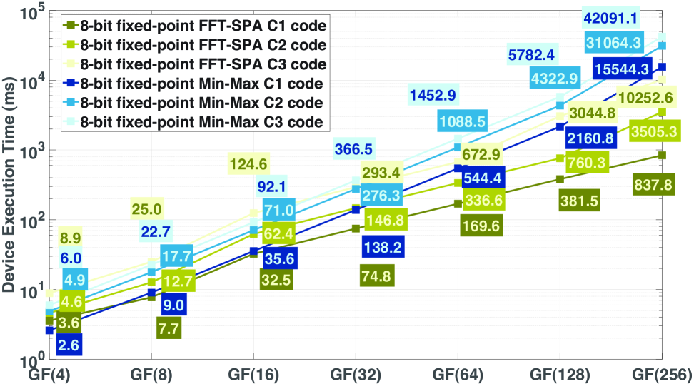
The experimental result shows similarities with the analysis performed in Fig. 5. As depicted in Fig. 6, the measured execution time in a single-threaded DRAM processing unit shows better scaling for the fast Fourier transform-sum-product algorithm. The min-max decoder has a faster execution time for smaller Galois fields but it is increases more than the fast Fourier transform-sum-product algorithm for larger codes and higher Galois fields.
The throughput performance is calculated using , where is the throughput performance measured in decoded bits per second, and is time. This formula ensures that the number of bits represented in each symbol is taken into account, giving the performance per decoded bit.
The following analysis follows a three-step approach to improve performance. The first step uses a single thread to implement the decoder in a single-DRAM processing unit. To improve results, the second step iterates over the first by employing multithreading with threads. The last step uses multicodewording, where several decoders from the previous step are launched concurrently in DRAM processing units with different codewords to decode.
The throughput values for the fast Fourier transform-sum-product algorithm with multithreading for are presented in Kbps. For -bit floating-point, they are , , and for , , and codes respectively. For -bit fixed-point, they are , , and for , , and codes respectively. In -bit fixed-point, the values are , , and . The performance decreases from to for every Galois field increment. The results show that for small Galois fields, the throughput increases for larger codes. However, for higher Galois fields, the performance decreases when the code size increases. This performance inversion happens at for -bit implementations and at for -bit implementations, suggesting that memory usage might impact multithreading implementations.
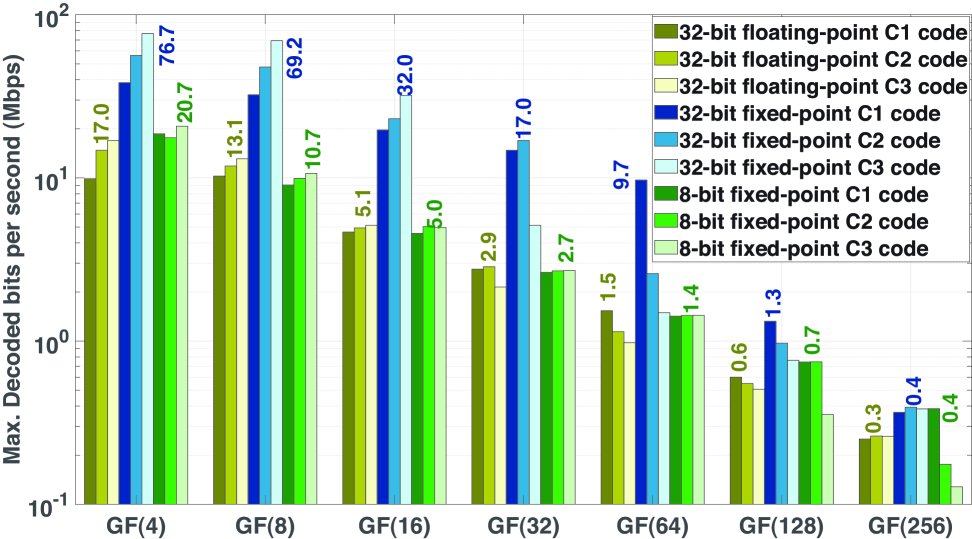
The maximum throughput for the -DRAM processing unit fast Fourier transform-sum-product algorithm decoders is Mbps using floating-point representation, Mbps using -bit integers, and Mbps using -bit integers, as shown in Fig. 7. The measured values represent the execution time between the first DRAM processing unit and the last.
However, changing from a -bit floating-point to a -bit integer benefits performance. In the single-DRAM processing unit multithreading setup, performance improves between for smaller Galois fields and for higher Galois fields. When comparing multi-DRAM processing unit, performance improves between for smaller Galois fields and .
When comparing the -bit with the -bit implementation for fast Fourier transform-sum-product algorithm, the performance in the single-DRAM processing unit multithreading setup improves up to . In the multi-DRAM processing unit setup, the performance decreases down to .
The multithreaded implementation of the min-max decoder processes different Galois fields in parallel. However, the pipeline is underutilized for and , resulting in reduced performance. The throughput values for the min-max with multithreading for are presented in Kbps and, for -bit are , , and for , , and codes respectively. For -bit, the values are , , and . For , the values increase by in average, and for the performance decreases by compared to . For higher fields, the performance decreases between and on average with each Galois field increment.
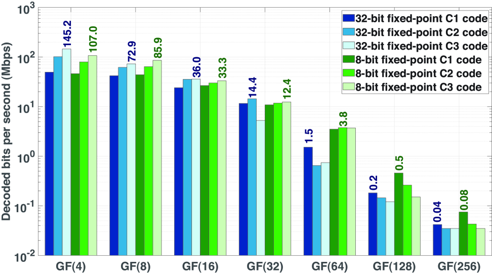
The maximum throughput for the -DRAM processing unit min-max decoder is Mbps using -bit integer representation, and Mbps using -bit integers, both in , as depicted in Fig. 8.
For this algorithm, changing from a -bit to an -bit implementation does not provide drastic differences in performance. The single-DRAM processing unit multithreading performance decreases between and for Galois fields below and improves up to for higher Galois fields. In the multi-DRAM processing unit implementation, the performance improves and degrades as in the previous observation.
The results for the -bit integer implementations show that DRAM processing units have underlying issues that prevent the exploitation of the capabilities of the computing units, namely pipeline masking issues since most of the performance is lost when using multithreading for kernels that execute in less than a couple of hundred milliseconds. Higher than this, -bit implementations tend to perform and scale better than their -bit integer counterparts. Furthermore, this effect seems particularly nefarious in multi-DRAM processing unit setups, especially for the fast Fourier transform-sum-product algorithm, where most kernels execute under ms.
5.3 Memory Transactions
To minimize the impact of costly data transfers between host and device, the chosen approach only transfers the codewords to and from the DRAM processing units and saves the graph topology in DRAM processing units without data transfers. The data is always saved in the faster working SRAM. However, the limited size of the working SRAM does not allow the saving of all data for larger codes in higher Galois fields. In this case, the buffer with fewer memory accesses is saved in main DRAM to maximize the number of memory accesses in working SRAM.
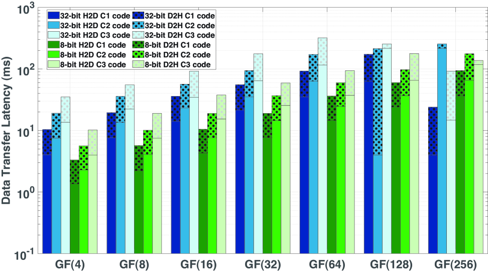
The use of main DRAM to save some of the buffers implies variations in the execution time for high Galois fields. The most prominent cases are shown in Fig. 9, for the -bit codeword in the code for and and also in the -bit codeword for in .
The transfer times of the received and decoded codewords are similar, since the size is the same (). For the -bit implementation, the transfer time is reduced for the same code size and Galois field. However, these times are greatly reduced when one or both of these buffers are saved in main DRAM. Since main DRAM is "closer" to the host, saving data in main DRAM is faster than saving data in working SRAM which requires the data to travel deeper in the memory hierarchy, taking more time.
For the fast Fourier transform-sum-product algorithm, Fig. 9 shows the time when transferring codewords for the available DRAM processing units. For the -bit implementation, in for the code, it takes between and to transfer one codeword from the host to the device, and and to transfer codewords, which means that several codewords are transferred at the same time. The transfer time increases between to when comparing a -bit codeword in single-DRAM processing unit to a multi-DRAM processing unit setup. For -bit codeword, the transfer times increase between to . Transferring from device to host also takes the same amount of time. Increasing the code size or Galois field doubles the transfer time (when compared to adjacent Galois fields or code sizes).
In Fig. 9, the transfer times (for -bit codewords) from host to device (solid bars) for the and codes in are much lower since the buffers are saved in main DRAM. The same happens for the code in . For transfers from device to host, and codes in save the output buffer in main DRAM, reducing transfer time by . For the code, the output buffer is saved in main DRAM for and .
In the -bit representation, besides reducing the transfer time by compared to -bit, only the output buffer of the code in is saved in main DRAM.
The values measured in the min-max decoder are similar to those in the fast Fourier transform-sum-product algorithm where saving data in main DRAM also produces the same effect.
5.4 Comparison to GPUs
Fig. 10 compares the fast Fourier transform-sum-product algorithm between UPMEM and low-power graphics processing units using a multithreading and multiple DRAM processing units -bit integer implementation. The UPMEM implementation can achieve Mbps for and Kbps for . The graphics processing unit values from [13] also present the maximum extractable performance, running decoders in parallel for the Jetson Nano, and decoders for TX and Xavier.
From this figure, the UPMEM system can be compared to a low-power graphics processing unit somewhere between a TX and Xavier. However, these graphics processing unit implementations can run more decoders in parallel, while the performance per core in the UPMEM system is higher than in graphics processing units.
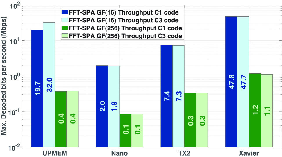
The limited nature of the UPMEM system, and processing-in-memory systems in general, does not allow the exploitation of some techniques used in graphics processing units. For instance, ordering the data has more benefits in graphics processing unit-based implementations, allowing coalesced memory accesses where several threads in the same warp access memory simultaneously. If memory accesses are not contiguous, threads in the same warp cannot access memory simultaneously, increasing overall memory access time.
In low-density parity-check codes, coalescing can be leveraged to increase performance by ordering the messages transmitted between the nodes. However, ordering the data for reading and/or writing for one type of node implies that the reads/writes for the other type of node are not contiguous. Coalescing mechanisms that allow the exploitation of bulk data transfers, are not present in the UPMEM system.
Furthermore, the UPMEM system does not feature caching mechanisms, unlike graphics processing units, that allow faster data access to increase performance. Instead, UPMEM features the working SRAM which is controlled by the programmer resulting in average faster slower data access times.
6 Key Takeaways
These decoder implementations and experimental results of this research, highlight the implications for in-memory low-density parity-check decoding and potential areas for future exploration for both parallel computing and coding theory communities. The main findings and observations of this work are:
-
•
First processing-in-memory-Based non-binary low-density parity-check Decoder Implementations: The paper introduces the first known processing-in-memory-based implementations of the fast Fourier transform-sum-product algorithm and the min-max algorithm for non-binary low-density parity-check decoding.
-
•
processing-in-memory Technology for low-density parity-check Decoding: The use of processing-in-memory technology, specifically the UPMEM system, can significantly alleviate the data movement bottleneck in non-binary low-density parity-check decoding, enhancing overall performance.
-
•
Competitive Throughput: The processing-in-memory-based non-binary low-density parity-check decoder achieves a decoding throughput of Mbit/s, making it competitive with edge graphics processing unit implementations.
-
•
Optimization Techniques: Effective optimization techniques, such as maximizing working SRAM usage, quantization, and loop unrolling, are crucial for enhancing the performance of low-density parity-check decoders on the UPMEM system.
-
•
Scalability and Modularity: The modular nature of the UPMEM system allows for scalable performance improvements by adding more processing-in-memory modules, unlike graphics processing units which require complete device replacements.
Efficient parallel computing requires understanding both software and hardware to fully exploit device capabilities. This work applies processing-in-memory technology to low-density parity-check decoding and offers recommendations for the parallel computing community:
7 Conclusion
This work highlights the potential of general-purpose processing-in-memory-based acceleration for non-binary low-density parity-check decoding using the UPMEM system. While individual DRAM processing unit cores in the UPMEM system are limited in performance, the parallel architecture and proximity to memory provide a significant advantage by reducing data movement bottlenecks. Although the UPMEM system may not fully match edge graphics processing units, it reaches performance levels comparable to low-power graphics processing units when executing fewer parallel decoders, indicating that performance is primarily constrained by the number of computing cores.
Furthermore, the modularity of the UPMEM system allows scalable performance improvements simply by adding more processing-in-memory modules, unlike graphics processing units which require complete device replacements for upgrades.
Overall, message quantization helps in achieving a balance between performance and resource utilization in low-density parity-check decoders, in particular those exploiting processing-in-memory-based functional units. Furthermore, this work demonstrates the feasibility of processing-in-memory-based non-binary low-density parity-check multicodeword decoding and provides valuable insights for future research, including new capability of processing larger datasets while moving less data, the adoption of more aggressive process node designs for supporting more complex operations, opening the door to broader applications like machine learning or image processing in this novel computing domain.
The proposed architecture is particularly well suited to high-density batch decoding environments, such as massive multiple-input multiple-output base stations, optical communication receivers, and cloud-radio access network infrastructure, where decoding hundreds or thousands of codewords in parallel is essential to meet data rate demands, despite the initial latency.
Acknowledgments
This work was supported by Instituto de Telecomunicações and FCT - Fundação para a Ciência e Tecnologia, I.P. by project reference 10.54499/UIDB/50008/2020, and DOI identifier https://doi.org/10.54499/UIDB/50008/2020, UIDP/50008/2020, 2022.06780.PTDC and Ph.D. grant 2020.07124.BD.
References
- [1] CCSDS. Short Block length LDPC codes for TC synchronization and channel coding. Orange book, 2015.
- [2] Peng Kang, Yixuan Xie, Lei Yang, and Jinhong Yuan. Enhanced Quasi-Maximum Likelihood Decoding Based on 2D Modified Min-Sum Algorithm for 5G LDPC Codes. IEEE Transactions on Communications, 68(11):6669–6682, 2020.
- [3] Hing-Mo Lam, Silin Lu, Hezi Qiu, Min Zhang, Hailong Jiao, and Shengdong Zhang. A High-Efficiency Segmented Reconfigurable Cyclic Shifter for 5G QC-LDPC Decoder. IEEE Transactions on Circuits and Systems I: Regular Papers, 69(1):401–414, 2022.
- [4] Haoran Xie, Yafeng Zhan, Guanming Zeng, and Xiaohan Pan. Leo mega-constellations for 6g global coverage: Challenges and opportunities. IEEE Access, 9:164223–164244, 2021.
- [5] Arijit Mondal and Shayan Srinivasa Garani. Efficient Parallel Decoding Architecture for Cluster Erasure Correcting 2-D LDPC Codes for 2-D Data Storage. IEEE Transactions on Magnetics, 57(12):1–16, 2021.
- [6] Meng Zhang, Fei Wu, Qin Yu, Neidong Fu, and Changsheng Xie. eLDPC: An Efficient LDPC Coding Scheme for Phase-Change Memory. IEEE Transactions on Computer-Aided Design of Integrated Circuits and Systems, 42(6):1978–1987, 2023.
- [7] M. C. Davey and D. J. C. MacKay. Low density parity check codes over GF(q). In Information Theory Workshop (Cat. No.98EX131), pages 70–71, 1998.
- [8] Harri Holma, Antti Toskala, and Takehiro Nakamura. 5G technology: 3GPP new radio. John Wiley & Sons, 2020.
- [9] Trung-Kien Le, Umer Salim, and Florian Kaltenberger. An overview of physical layer design for ultra-reliable low-latency communications in 3gpp releases 15, 16, and 17. IEEE Access, 9:433–444, 2021.
- [10] Bertrand Le Gal and Christophe Jego. Low-latency software LDPC decoders for x86 multi-core devices. In 2017 IEEE International Workshop on Signal Processing Systems (SiPS), pages 1–6, 2017.
- [11] Bertrand Le Gal and Christophe Jego. High-throughput fft-spa decoder implementation for non-binary ldpc codes on x86 multicore processors. Journal of Signal Processing Systems, 92:37–53, 2020.
- [12] Guohui Wang, Hao Shen, Bei Yin, Michael Wu, Yang Sun, and Joseph R Cavallaro. Parallel nonbinary LDPC decoding on GPU. In 2012 46th Asilomar Conference on Signals, Systems and Computers (ASILOMAR), pages 1277–1281. IEEE, 2012.
- [13] Oscar Ferraz, Vitor Silva, and Gabriel Falcao. On the Performance of Link Space Communications using NB-LDPC Codes on Embedded Parallel Systems. In 2021 55th Asilomar Conference on Signals, Systems, and Computers, pages 1164–1168. IEEE, 2021.
- [14] Jiaming Liu and Quanyuan Feng. A Miniaturized LDPC Encoder: Two-Layer Architecture for CCSDS Near-Earth Standard. IEEE Transactions on Circuits and Systems II: Express Briefs, 68(7):2384–2388, 2021.
- [15] Jérémy Nadal and Amer Baghdadi. Parallel and Flexible 5G LDPC Decoder Architecture Targeting FPGA. IEEE Transactions on Very Large Scale Integration (VLSI) Systems, 29(6):1141–1151, 2021.
- [16] Oscar Ferraz, Srinivasan Subramaniyan, Ramesh Chinthalaa, João Andrade, Joseph R. Cavallaro, Soumitra K. Nandy, Vitor Silva, Xinmiao Zhang, Madhura Purnaprajna, and Gabriel Falcao. A Survey on High-Throughput Non-Binary LDPC Decoders: ASIC, FPGA and GPU Architectures. IEEE Communications Surveys & Tutorials, pages 1–1, 2021.
- [17] Thien Truong Nguyen-Ly, Valentin Savin, Khoa Le, David Declercq, Fakhreddine Ghaffari, and Oana Boncalo. Analysis and design of cost-effective, high-throughput LDPC decoders. IEEE Transactions on Very Large Scale Integration (VLSI) Systems, 26(3):508–521, 2017.
- [18] R. Gallager. Low-density parity-check codes. IRE Transactions on Information Theory, 8(1):21–28, 1962.
- [19] Dan Feng, Hengzhou Xu, Qiang Zhang, Qian Li, Yucheng Qu, and Baoming Bai. Nonbinary ldpc-coded modulation system in high-speed mobile communications. IEEE Access, 6:50994–51001, 2018.
- [20] Shuai Shao, Peter Hailes, Tsang-Yi Wang, Jwo-Yuh Wu, Robert G Maunder, Bashir M Al-Hashimi, and Lajos Hanzo. Survey of Turbo, LDPC, and Polar Decoder ASIC Implementations. IEEE Communications Surveys & Tutorials, 21(3):2309–2333, 2019.
- [21] Nika Mansouri Ghiasi, Nandita Vijaykumar, Geraldo F. Oliveira, Lois Orosa, Ivan Fernandez, Mohammad Sadrosadati, Konstantinos Kanellopoulos, Nastaran Hajinazar, Juan Gómez Luna, and Onur Mutlu. ALP: Alleviating CPU-Memory Data Movement Overheads in Memory-Centric Systems. IEEE Transactions on Emerging Topics in Computing, 11(2):388–403, 2023.
- [22] Onur Mutlu, Saugata Ghose, Juan Gómez-Luna, and Rachata Ausavarungnirun. A modern primer on processing in memory. In Emerging Computing: From Devices to Systems: Looking Beyond Moore and Von Neumann, pages 171–243. Springer, 2022.
- [23] Maryam S. Hosseini, Masoumeh Ebrahimi, Pooria Yaghini, and Nader Bagherzadeh. Near Volatile and Non-Volatile Memory Processing in 3D Systems. IEEE Transactions on Emerging Topics in Computing, 10(3):1657–1664, 2022.
- [24] Purab Ranjan Sutradhar, Sathwika Bavikadi, Sai Manoj Pudukotai Dinakarrao, Mark A. Indovina, and Amlan Ganguly. 3DL-PIM: A Look-Up Table Oriented Programmable Processing in Memory Architecture Based on the 3-D Stacked Memory for Data-Intensive Applications. IEEE Transactions on Emerging Topics in Computing, 12(1):60–72, 2024.
- [25] Changwu Zhang, Hao Sun, Shuman Li, Yaohua Wang, Haiyan Chen, and Hengzhu Liu. A Survey of Memory-Centric Energy Efficient Computer Architecture. IEEE Transactions on Parallel and Distributed Systems, 34(10):2657–2670, 2023.
- [26] Yueting Li, Tianshuo Bai, Xinyi Xu, Yundong Zhang, Bi Wu, Hao Cai, Biao Pan, and Weisheng Zhao. A Survey of MRAM-Centric Computing: From Near Memory to In Memory. IEEE Transactions on Emerging Topics in Computing, 11(2):318–330, 2023.
- [27] Juan Gómez-Luna, Izzat El Hajj, Ivan Fernandez, Christina Giannoula, Geraldo F Oliveira, and Onur Mutlu. Benchmarking a new paradigm: An experimental analysis of a real processing-in-memory architecture. arXiv preprint arXiv:2105.03814, 2021.
- [28] Daichi Fujiki, Scott Mahlke, and Reetuparna Das. Duality cache for data parallel acceleration. In Proceedings of the 46th International Symposium on Computer Architecture, pages 397–410, 2019.
- [29] Vivek Seshadri, Donghyuk Lee, Thomas Mullins, Hasan Hassan, Amirali Boroumand, Jeremie Kim, Michael A Kozuch, Onur Mutlu, Phillip B Gibbons, and Todd C Mowry. Buddy-RAM: Improving the performance and efficiency of bulk bitwise operations using DRAM. arXiv preprint arXiv:1611.09988, 2016.
- [30] Shaahin Angizi, Zhezhi He, and Deliang Fan. PIMA-logic: A novel processing-in-memory architecture for highly flexible and energy-efficient logic computation. In Proceedings of the 55th Annual Design Automation Conference, pages 1–6, 2018.
- [31] Vivek Seshadri, Donghyuk Lee, Thomas Mullins, Hasan Hassan, Amirali Boroumand, Jeremie Kim, Michael A Kozuch, Onur Mutlu, Phillip B Gibbons, and Todd C Mowry. Ambit: In-memory accelerator for bulk bitwise operations using commodity DRAM technology. In Proceedings of the 50th Annual IEEE/ACM International Symposium on Microarchitecture, pages 273–287, 2017.
- [32] UPMEM. Introduction to UPMEM PIM. Processing-in-memory (PIM) on DRAM Accelerator (White Paper). 2018.
- [33] CCSDS. TC Synchronization and Channel Coding. In CCSDS 231.0-B-3, 2017.
- [34] Yifei Shen, Yuqing Ren, Andreas Toftegaard Kristensen, Xiaohu You, Chuan Zhang, and Andreas Burg. Improved Belief Propagation Decoding of Turbo Codes. In ICASSP 2023 - 2023 IEEE International Conference on Acoustics, Speech and Signal Processing (ICASSP), pages 1–5, 2023.
- [35] Judea Pearl. Fusion, Propagation, and Structuring in Belief Networks, page 139–188. Association for Computing Machinery, New York, NY, USA, 1 edition, 2022.
- [36] Nassim Douali, Huszka Csaba, Jos De Roo, Elpiniki I. Papageorgiou, and Marie-Christine Jaulent. Diagnosis Support System based on clinical guidelines: comparison between Case-Based Fuzzy Cognitive Maps and Bayesian Networks. Computer Methods and Programs in Biomedicine, 113(1):133–143, 2014.
- [37] José Vinícius de M Cardoso, Jiaxi Ying, and Daniel P Palomar. Nonconvex graph learning: sparsity, heavy tails, and clustering. In Signal Processing and Machine Learning Theory, pages 1049–1072. Elsevier, 2024.
- [38] Rolando Antonio Carrasco and Martin Johnston. Non-binary error control coding for wireless communication and data storage. John Wiley & Sons, 2008.
- [39] L. Barnault and D. Declercq. Fast decoding algorithm for LDPC over . In Proceedings 2003 IEEE Information Theory Workshop (Cat. No.03EX674), pages 70–73, 2003.
- [40] Yajing Chen, Shengshuo Lu, Cheng Fu, David Blaauw, Ronald Dreslinski, Trevor Mudge, and Hun-Seok Kim. A Programmable Galois Field Processor for the Internet of Things. SIGARCH Comput. Archit. News, 45(2):55–68, June 2017.
- [41] V. Savin. Min-Max decoding for non binary LDPC codes. In 2008 IEEE International Symposium on Information Theory, pages 960–964, 2008.
- [42] Fabrice Devaux. The true Processing In Memory accelerator. In 2019 IEEE Hot Chips 31 Symposium (HCS), pages 1–24, 2019.
- [43] UPMEM. UPMEM User Manual. Accessed: June. 2024 [Online]. Available: https://sdk.upmem.com/2021.4.0/index.html.
- [44] Oscar Ferraz, Yann Falevoz, Vitor Silva, and Gabriel Falcao. Unlocking the Potential of LDPC Decoders with PiM Acceleration. In 2023 57th Asilomar Conference on Signals, Systems, and Computers, pages 1579–1583, 2023.
- [45] Oscar Ferraz, Gabriel Falcao, and Vitor Silva. In-Memory Bit Flipping LDPC Decoding. In 2024 32nd European Signal Processing Conference (EUSIPCO), 2024.
- [46] Bertrand Le Gal and Christophe Jego. High-Throughput Multi-Core LDPC Decoders Based on x86 Processor. IEEE Transactions on Parallel and Distributed Systems, 27(5):1373–1386, 2016.
- [47] Henk Wymeersch, Heidi Steendam, and Marc Moeneclaey. Computational complexity and quantization effects of decoding algorithms for non-binary ldpc codes. In 2004 IEEE International Conference on Acoustics, Speech, and Signal Processing, volume 4, pages iv–iv. IEEE, 2004.
- [48] Joao Andrade, Gabriel Falcao, Vitor Silva, and Kenta Kasai. FFT-SPA non-binary LDPC decoding on GPU. In 2013 IEEE International Conference on Acoustics, Speech and Signal Processing, pages 5099–5103. IEEE, 2013.
- [49] D. Declercq and M. Fossorier. Decoding Algorithms for Nonbinary LDPC Codes Over . IEEE Transactions on Communications, 55(4):633–643, 2007.