Engineering Ge profiles in Si/SiGe heterostructures for increased valley splitting
Abstract
Electron spin qubits in Si/SiGe quantum wells are limited by the small and variable energy separation of the conduction band valleys. While sharp quantum well interfaces are pursued to increase the valley splitting energy deterministically, here we explore an alternative approach to enhance the valley splitting on average. We grow increasingly thinner quantum wells with broad interfaces to controllably increase the overlap of the electron wave function with Ge atoms. In these quantum wells, comprehensive quantum Hall measurements of two-dimensional electron gases reveal a linear correlation between valley splitting and disorder. Benchmarked against quantum wells with sharp interfaces, we demonstrate enhanced valley splitting while maintaining a low-disorder potential environment. Simulations using the experimental Ge concentration profiles predict an average valley splitting in quantum dots that matches the enhancement observed in two-dimensional systems. Our results motivate the experimental realization of quantum dot spin qubits in these heterostructures.
QuTech] QuTech and Kavli Institute of Nanoscience, Delft University of Technology, Lorentzweg 1, 2628 CJ Delft, The Netherlands QuTech] QuTech and Kavli Institute of Nanoscience, Delft University of Technology, Lorentzweg 1, 2628 CJ Delft, The Netherlands QuTech] QuTech and Kavli Institute of Nanoscience, Delft University of Technology, Lorentzweg 1, 2628 CJ Delft, The Netherlands \alsoaffiliationICREA, Pg. Lluís Companys 23, 08010 Barcelona, Catalonia, Spain QuTech] QuTech and Kavli Institute of Nanoscience, Delft University of Technology, Lorentzweg 1, 2628 CJ Delft, The Netherlands
1 Introduction
Spin qubit devices in gate-defined Si/SiGe quantum dots have advanced in performance, qubit count, and connectivity. Reproducible single- and two-qubit gate fidelities exceeding 99% have been achieved 1, 2, 3. Moreover, linear array devices have scaled the number of qubits from six 4 to twelve 5, and a two-by-two qubit array has been demonstrated6. Coherent, high fidelity spin shuttling 7, 8, 9 and cavity-mediated iSWAP oscillations between distant spins 10 are promising achievements for connectivity beyond nearest neighbour. In addition, the fabrication of Si/SiGe spin qubits in a 300 mm semiconductor manufacturing facility 11 and the integration of multi-level interconnects with 2D spin qubit arrays 12 underscore the potential for scalable architectures. Despite this compelling progress, critical material challenges remain in the pursuit of a large-scale quantum computer.
In Si/SiGe heterostructures, a long-standing limitation has been the small and variable energy splitting between the two low-lying conduction band valleys 13, 14. In quantum dots, the reported valley energy splittings vary between a few tens to hundreds of eV 15, 16, 17, 18, 19, 20, 21, 22. This poses a challenge for spin qubits, because the increased leakage from the computational two-level Hilbert space affects high-fidelity initialization, control, readout, and shuttling 23, 24, 25, 26, 27, 28, 29.
Recent work combining experiments and theory30, 31 has established that the atomistic random alloy concentration fluctuations at the Si/SiGe interface are accountable for the measured valley splitting spread in real quantum dots. Furthermore, the valley splitting is expected to be enhanced when the electronic wavefunction overlaps with more Ge atoms. While proposed strategies like intentionally adding Ge to the Si quantum well promise increased valley splitting 30, 31, they may also worsen disorder, affecting electron mobility 20. However, careful tuning of the germanium concentration profile–through adjustments in the Si quantum well thickness, interface width, and barrier composition–can strike a delicate balance between achieving high valley splitting and maintaining low disorder 32.
Here, we engineer the Ge concentration profiles of 28Si/28SiGe heterostructures to enhance the overlap of the electron wave function with Ge atoms in a tunable way, by growing increasingly thin quantum wells with intentionally diffused interfaces. We characterize the Ge concentration profiles by atomic-resolution scanning transmission electron microscopy (STEM), while we measure the mobility and valley splitting energy of the two-dimensional electron gas () by comprehensive density-dependent magnetotransport. Benchmarking against control heterostructures with sharp interfaces 32, we can controllably increase valley splitting by up to a factor of two. Although we unambiguously observe that higher valley splitting correlates with increased electrical disorder, a beneficial trade-off between enhanced valley splitting and low disorder is achievable. Furthermore, simulations of quantum dot valley splitting energy () based on the experimental Ge concentration profiles, reveal a linear relationship with . This finding provides a first insight into the long-sought connection between valley splitting in the quantum Hall regime and in quantum dots.
2 Results and discussion

Figures 1(a)-(c) show atomic-resolution high angle annular dark field (HAADF) STEM images of three 28Si/28SiGe heterostructures (B1–B3) having progressively thinner quantum wells with similarly broad interfaces. As a control, Fig. 1(d) shows 28Si/SiGe heterostructure (A), with sharp interfaces as studied in 32. Broad interfaces in heterostructures B1–B3 result from uninterrupted epitaxy at a temperature of 750 °C using only hydride precursors (28SiH4, GeH4). In contrast, sharp interfaces in heterostructure A are achieved by growing the SiGe barriers at a lower temperature of 625 °C, enabled by using a different Si precursor (SiH2Cl2) 30, 32. In all heterostructures, the quantum well is deposited on a SiGe strain-relaxed buffer and is separated from the dielectric interface by a 30 nm SiGe barrier (see Section 1 in the Supporting Information). Due to the different gas precursors, heterostructures B1–B3 feature an isotopically-enriched barrier with a slightly lower Ge concentration () compared to heterostructure A (). The small difference in chemical composition, and therefore band offset, is confirmed by electrical measurements of the quantum well saturation charge density 33, 34, which is smaller in B1–B3 compared to A (see Fig. S1 in the Supporting Information). In Fig. 1(e) we show the Ge concentration profiles from A (left panel) and B1–B3 (right panel) extracted from the HAADF-STEM images (see Fig. S1 in the Supporting Information). The right panel highlights both the reproducibility of the growth process from the overlapping bottom interfaces ( nm) as well as the control over the quantum well width. From the concentration profiles, we extract the quantum well width and the width of the top and bottom interfaces. Table 1 gives a quantitative overview of the extracted parameters. We controllably reduce the quantum well width between the heterostructures B1–B3 by adjusting the quantum well growth time. Notably, the interfaces of heterostructures B1–B3 are approximately 2.4 times wider than those of heterostructure A.
| A | B1 | B2 | B3 | |
|---|---|---|---|---|
| (nm) | 6.9 | 9.5 | 7.8 | 5.9 |
| (nm) | 1.5 | 3.7 | 3.7 | 3.6 |
| (nm) | 1.6 | 3.3 | 3.5 | 3.5 |
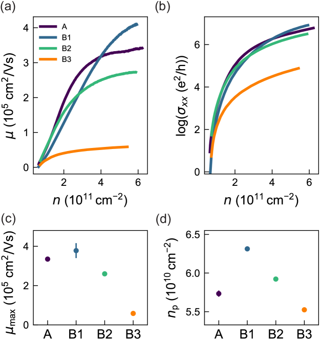
We evaluate the disorder properties of the two-dimensional electron gas (2DEG) in each heterostructure by fabricating Hall-bar-shaped heterostructure field effect transistors (H-FETs) and performing magnetotransport measurements at 70 mK in a dilution refrigerator equipped with a cryo-multiplexer 35 (see Section 4 in the Supporting Information). Figures 2(a),(b) show the mobility-density and conductivity-density curves of a representative H-FET for each heterostructure (see Fig. S2 in the Supporting Information for other H-FETs). Heterostructures A, B1, and B2 show similar mobility-density curves, while heterostructure B3 shows a severe suppression of the mobility across the entire density range. In Fig. 2(c) we show the average extracted mobility for each heterostructure. Maximum mobility decreases from in B1 to in B3 as the quantum well becomes increasingly thinner. Compared to the control heterostructure A, B1 shows a higher average maximum mobility which we attribute to the increased growth temperature resulting in decreased background contamination. However, B1 also shows a larger spread across multiple H-FETs which is indicative of the onset of strain relaxation within the quantum well, creating additional scattering centres from dislocations 19, 32. The severe reduction of maximum mobility in B3 is compatible with the presence of Ge throughout the thin quantum well. 36, 37, 38.
In contrast to the observed trend in maximum mobility, we do not observe a strong dependence across different heterostructures of the percolation density (Fig. 2(d)), obtained by fitting the conductivity curves in Fig. 2(b) (see Section 4 in the Supporting Information). We find similar low values of around for all heterostructures within the constraints of the fitting procedure, which is consistent with previous arguments that alloy disorder only weakly affects the scattering rate at low density 36, 37, 38. This observation suggests that the increased disorder from the diffusion of the interfaces does not severely affect the disorder properties of the 2DEG in the low-density regime, which is relevant for quantum dots.
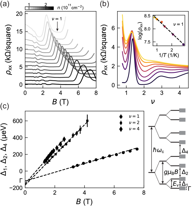
After assessing disorder in the heterostructures, we probe valley splitting in the same H-FETs by performing activation energy measurements in the quantum Hall regime, following Ref. 39 . We focus on the first valley-split energy gap () at filling factor , since this gap is resolved across all heterostructures over a similar range of density and magnetic field , enabling meaningful comparisons. Additionally, we measure the first Zeeman-split gap (), and first Landau gap (), corresponding to , and , respectively. Figure 3 illustrates the measurement protocol with data from heterostructure B2, while measurements from all other heterostructures are shown in Figs. S3–S5 in the Supporting Information. First, we measure the longitudinal resistivity at base temperature as a function of , over a range of fixed densities (Fig. 3(a)). We observe clear Shubnikov de Haas oscillations, with minima at reaching zero, indicating a well resolved . For each , we repeat the measurement for different temperatures () and plot in Fig. 3(b) as a function of filling factor , given by the quantum Hall relation , where is the Planck’s constant and the electron charge. As the inset shows for , we observe a thermally activated dependence of the oscillation minima (). For each density, we extract the valley-split, Zeeman split and Landau mobility gaps (, , respectively), plotted in Fig. 3(c) as a function of magnetic field . As in Ref. 39 , we observe striking linear relationships converging to a similar intercept, from which we estimate with confidence the Landau level broadening-induced disorder (Fig. 3(c), side panel) and the valley splitting .
Following this systematic classical and quantum transport characterization, we may now investigate the key link between valley splitting and disorder, underpinned by the engineered Ge concentration profiles in the different heterostructures. In all heterostructures, increases linearly with across the investigated range (Fig. 4(a)). Additionally, the top -axis shows the correspondingly increasing orbital energy, , where we use an in-plane effective mass of for electrons in Si. Note that the relation was previously observed 39, 40 and attributed 39 to the stronger electrostatic confinement achieved for a higher density in the quantum Hall edge channel, driven by via the quantum Hall relation for .
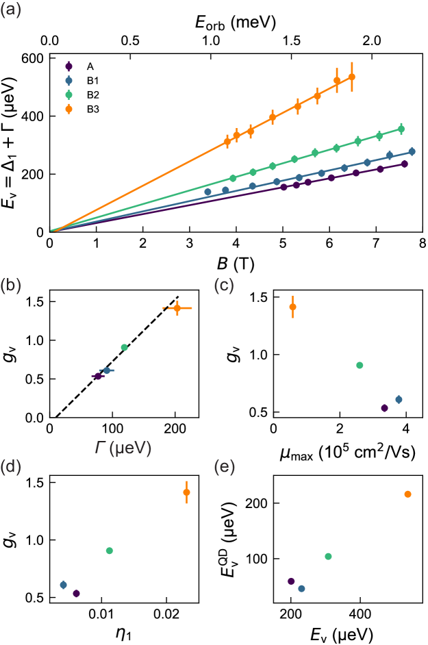
Across the explored magnetic field range, we observe a clear trend in Fig. 4(a): all heterostructures with broad interfaces (B1–B3) show larger valley splitting compared to the control heterostructure A. Moreover, within heterostructures B1–B3, thinner quantum wells achieve larger valley splitting, validating our heterostructure design. To quantify these observations, we extract the valley -factor, , which represents the rate of change of valley splitting with magnetic field, normalized to the Bohr magneton . Figure 4(b) shows against the disorder-induced Landau level broadening , revealing a striking experimental correlation, further corroborated in Figure 4(c) by the dependence of against the maximum mobility. The valley splitting in heterostructures B1–B3 may increase to more than twice the value observed in the control heterostructure A. These clear trends confirm the intuition that increasing valley splitting, which requires breaking translation symmetry, comes at the expense of a more disordered potential landscape 31, 32, qualified in our experiments either by classical or quantum transport measurements.
Next, we investigate the atomistic origin of the increased valley splitting and provide a prognosis for potential gains for valley splitting in quantum dots. To this end, we calculate for each heterostructure the parameter (see Section 5 in the Supporting Information), which quantifies the overlap of the electron wave function with Ge atoms, and simulate the quantum dot valley splitting distributions and their mean value . We use the extracted Ge concentration profiles of Fig. 1(e) as an experimental input for the simulation methods in Ref. 31 . As Fig. 4(d) shows, we find an unambiguous correlation between and , suggesting that the larger measured in the 2DEG correlates with increased overlap of the electron wave function with Ge atoms, promoted in our experiments by thinner quantum wells with broad interfaces. This finding () mirrors the theoretical predictions for average valley splitting in alloy disorder-dominated quantum dots ( (see Section 5 in the Supporting Information and Refs.30, 31). As a consequence, the plot in Fig. 4(e) of simulated against experimentally measured shows also a linear relationship. Here, we choose to simulate at an orbital energy of 1.88 meV, which is on par with measured values in quantum dots and corresponds from Fig. 4(a) to an experimentally accessible magnetic field of 6.5 T for evaluation of . Considering the same orbital energy ensures a meaningful comparison between the experimentally-informed simulation of and the measured . While offering a first insight into the relation between the two metrics, based on these results we predict that heterostructures B1–B3 could support on average increased valley splitting in quantum dots, which is proxied by valley splitting measured in the quantum Hall regime.
3 Conclusions
In summary, we have engineered heterostructures to enhance the overlap of the electron wave function with germanium atoms, by growing increasingly thin quantum wells with intentionally diffused interfaces. Our comprehensive study unveils unambiguously a correlation between disorder in the two-dimensional electron gas, measured with classical and quantum transport, and valley splitting, measured in the quantum Hall regime. Valley splitting is increased but so is disorder. Based on simulations that take into account the experimental Ge concentration profile, we identify the overlap of the electron wavefunction with Ge atoms as the likely cause of this connection, which also propagates to calculated average values of valley splitting distributions in quantum dots.
Compared to control samples with sharp interfaces in Ref. 32 , we show that a quantum well with much broader interfaces (3.6 nm) and similar width ( nm) offers an excellent trade-off, featuring a valley splitting increase, whilst still having respectable mobility ( cm2/Vs) and low percolation density ( cm-2). In contrast, thinner or thicker quantum wells either significantly degrade mobility or yield only marginal improvements in valley splitting. Future statistical studies of valley splitting in quantum dots fabricated on these new generations of heterostructures are required to confirm the valley splitting increase and assess the impact of random alloy disorder in the formation of spurious quantum dots.
4 Acknowledgments
This work was supported by the Netherlands Organisation for Scientific Research (NWO/OCW), via the Frontiers of Nanoscience program Open Competition Domain Science - M program. We acknowledge support by the European Union through the IGNITE project with grant agreement No. 101069515 and the QLSI project with grant agreement No. 951852. This research was sponsored in part by the Army Research Office (ARO) under Awards No. W911NF-23-1-0110 and W911NF-22-1-0090 . The views, conclusions, and recommendations contained in this document are those of the authors and are not necessarily endorsed nor should they be interpreted as representing the official policies, either expressed or implied, of the Army Research Office (ARO) or the U.S. Government. The U.S. Government is authorized to reproduce and distribute reprints for Government purposes notwithstanding any copyright notation herein. This research was sponsored in part by The Netherlands Ministry of Defence under Awards No. QuBits R23/009. The views, conclusions, and recommendations contained in this document are those of the authors and are not necessarily endorsed nor should they be interpreted as representing the official policies, either expressed or implied, of The Netherlands Ministry of Defence. The Netherlands Ministry of Defence is authorized to reproduce and distribute reprints for Government purposes notwithstanding any copyright notation herein. ICN2 acknowledges funding from Generalitat de Catalunya 2021SGR00457. We acknowledge support from CSIC Interdisciplinary Thematic Platform (PTI+) on Quantum Technologies (PTI-QTEP+). This research work has been funded by the European Commission – NextGenerationEU (Regulation EU 2020/2094), through CSIC’s Quantum Technologies Platform (QTEP). ICN2 is supported by the Severo Ochoa program from Spanish MCIN / AEI (Grant No.: CEX2021-001214-S) and is funded by the CERCA Programme / Generalitat de Catalunya. Authors acknowledge the use of instrumentation as well as the technical advice provided by the Joint Electron Microscopy Center at ALBA (JEMCA). ICN2 acknowledges funding from Grant IU16-014206 (METCAM-FIB) funded by the European Union through the European Regional Development Fund (ERDF), with the support of the Ministry of Research and Universities, Generalitat de Catalunya.
Data availability
The data sets supporting the findings of this study are openly available in 4TU Research Data at \urlhttps://doi.org/10.4121/ebcf5563-628e-479c-9e0d-d5094ebb9c27.
References
- Xue et al. 2022 Xue, X.; Russ, M.; Samkharadze, N.; Undseth, B.; Sammak, A.; Scappucci, G.; Vandersypen, L. M. K. Quantum logic with spin qubits crossing the surface code threshold. Nature 2022, 601, 343–347
- Noiri et al. 2022 Noiri, A.; Takeda, K.; Nakajima, T.; Kobayashi, T.; Sammak, A.; Scappucci, G.; Tarucha, S. Fast universal quantum gate above the fault-tolerance threshold in silicon. Nature 2022, 601, 338–342
- Mills et al. 2022 Mills, A. R.; Guinn, C. R.; Gullans, M. J.; Sigillito, A. J.; Feldman, M. M.; Nielsen, E.; Petta, J. R. Two-qubit silicon quantum processor with operation fidelity exceeding 99
- Philips et al. 2022 Philips, S. G. J.; Madzik, M. T.; Amitonov, S. V.; de Snoo, S. L.; Russ, M.; Kalhor, N.; Volk, C.; Lawrie, W. I. L.; Brousse, D.; Tryputen, L.; Wuetz, B. P.; Sammak, A.; Veldhorst, M.; Scappucci, G.; Vandersypen, L. M. K. Universal control of a six-qubit quantum processor in silicon. Nature 2022, 609, 919–924
- George et al. 2025 George, H. C. et al. 12-Spin-Qubit Arrays Fabricated on a 300 mm Semiconductor Manufacturing Line. Nano Letters 2025, 25, 793–799
- Unseld et al. 2024 Unseld, F. K.; Undseth, B.; Raymenants, E.; Matsumoto, Y.; Karwal, S.; Pietx-Casas, O.; Ivlev, A. S.; Meyer, M.; Sammak, A.; Veldhorst, M.; Scappucci, G.; Vandersypen, L. M. K. Baseband control of single-electron silicon spin qubits in two dimensions. 2024
- Noiri et al. 2022 Noiri, A.; Takeda, K.; Nakajima, T.; Kobayashi, T.; Sammak, A.; Scappucci, G.; Tarucha, S. A shuttling-based two-qubit logic gate for linking distant silicon quantum processors. Nature Communications 2022, 13
- Seidler et al. 2022 Seidler, I.; Struck, T.; Xue, R.; Focke, N.; Trellenkamp, S.; Bluhm, H.; Schreiber, L. R. Conveyor-mode single-electron shuttling in Si/SiGe for a scalable quantum computing architecture. npj Quantum Information 2022, 8
- De Smet et al. 2024 De Smet, M.; Matsumoto, Y.; Zwerver, A.-M. J.; Tryputen, L.; de Snoo, S. L.; Amitonov, S. V.; Sammak, A.; Samkharadze, N.; Gül, Ö.; Wasserman, R. N. M.; Rimbach-Russ, M.; Scappucci, G.; Vandersypen, L. M. K. High-fidelity single-spin shuttling in silicon. 2024
- Dijkema et al. 2025 Dijkema, J.; Xue, X.; Harvey-Collard, P.; Rimbach-Russ, M.; de Snoo, S. L.; Zheng, G.; Sammak, A.; Scappucci, G.; Vandersypen, L. M. K. Cavity-mediated iSWAP oscillations between distant spins. Nature Physics 2025, 21, 168–174
- Neyens et al. 2024 Neyens, S. et al. Probing single electrons across 300-mm spin qubit wafers. Nature 2024, 629, 80–85
- Ha et al. 2025 Ha, S. D. et al. Two-dimensional Si spin qubit arrays with multilevel interconnects. 2025; \urlhttp://arxiv.org/abs/2502.08861, arXiv:2502.08861
- Friesen et al. 2006 Friesen, M.; Eriksson, M. A.; Coppersmith, S. N. Magnetic field dependence of valley splitting in realistic Si/SiGe quantum wells. Applied Physics Letters 2006, 89, 202106
- Zwanenburg et al. 2013 Zwanenburg, F. A.; Dzurak, A. S.; Morello, A.; Simmons, M. Y.; Hollenberg, L. C. L.; Klimeck, G.; Rogge, S.; Coppersmith, S. N.; Eriksson, M. A. Silicon quantum electronics. Rev. Mod. Phys. 2013, 85, 961–1019
- Maune et al. 2012 Maune, B. M.; Borselli, M. G.; Huang, B.; Ladd, T. D.; Deelman, P. W.; Holabird, K. S.; Kiselev, A. A.; Alvarado-Rodriguez, I.; Ross, R. S.; Schmitz, A. E.; Sokolich, M.; Watson, C. A.; Gyure, M. F.; Hunter, A. T. Coherent singlet-triplet oscillations in a silicon-based double quantum dot. Nature 2012, 481, 344–347
- Zajac et al. 2015 Zajac, D. M.; Hazard, T. M.; Mi, X.; Wang, K.; Petta, J. R. A reconfigurable gate architecture for Si/SiGe quantum dots. Applied Physics Letters 2015, 106
- Shi et al. 2011 Shi, Z.; Simmons, C. B.; Prance, J. R.; King Gamble, J.; Friesen, M.; Savage, D. E.; Lagally, M. G.; Coppersmith, S. N.; Eriksson, M. A. Tunable singlet-triplet splitting in a few-electron Si/SiGe quantum dot. Applied Physics Letters 2011, 99
- Scarlino et al. 2017 Scarlino, P.; Kawakami, E.; Jullien, T.; Ward, D. R.; Savage, D. E.; Lagally, M. G.; Friesen, M.; Coppersmith, S. N.; Eriksson, M. A.; Vandersypen, L. M. K. Dressed photon-orbital states in a quantum dot: Intervalley spin resonance. Physical Review B 2017, 95, 165429
- Paquelet Wuetz et al. 2023 Paquelet Wuetz, B.; Degli Esposti, D.; Zwerver, A.-M. J.; Amitonov, S. V.; Botifoll, M.; Arbiol, J.; Vandersypen, L. M. K.; Russ, M.; Scappucci, G. Reducing charge noise in quantum dots by using thin silicon quantum wells. Nature Communications 2023, 14
- McJunkin et al. 2022 McJunkin, T.; Harpt, B.; Feng, Y.; Losert, M. P.; Rahman, R.; Dodson, J. P.; Wolfe, M. A.; Savage, D. E.; Lagally, M. G.; Coppersmith, S. N.; Friesen, M.; Joynt, R.; Eriksson, M. A. SiGe quantum wells with oscillating Ge concentrations for quantum dot qubits. Nature Communications 2022, 13
- Hollmann et al. 2020 Hollmann, A.; Struck, T.; Langrock, V.; Schmidbauer, A.; Schauer, F.; Leonhardt, T.; Sawano, K.; Riemann, H.; Abrosimov, N. V.; Bougeard, D.; Schreiber, L. R. Large, Tunable Valley Splitting and Single-Spin Relaxation Mechanisms in a Si/ Quantum Dot. Physical Review Applied 2020, 13, 034068
- Borselli et al. 2011 Borselli, M. G.; Ross, R. S.; Kiselev, A. A.; Croke, E. T.; Holabird, K. S.; Deelman, P. W.; Warren, L. D.; Alvarado-Rodriguez, I.; Milosavljevic, I.; Ku, F. C.; Wong, W. S.; Schmitz, A. E.; Sokolich, M.; Gyure, M. F.; Hunter, A. T. Measurement of valley splitting in high-symmetry Si/SiGe quantum dots. Applied Physics Letters 2011, 98
- Vandersypen et al. 2017 Vandersypen, L. M. K.; Bluhm, H.; Clarke, J. S.; Dzurak, A. S.; Ishihara, R.; Morello, A.; Reilly, D. J.; Schreiber, L. R.; Veldhorst, M. Interfacing spin qubits in quantum dots and donors—hot, dense, and coherent. npj Quantum Information 2017, 3, 1–10
- Tagliaferri et al. 2018 Tagliaferri, M. L. V.; Bavdaz, P. L.; Huang, W.; Dzurak, A. S.; Culcer, D.; Veldhorst, M. Impact of valley phase and splitting on readout of silicon spin qubits. Physical Review B 2018, 97, 245412
- Huang and Hu 2014 Huang, P.; Hu, X. Spin relaxation in a Si quantum dot due to spin-valley mixing. Physical Review B 2014, 90, 235315
- Seidler et al. 2022 Seidler, I.; Struck, T.; Xue, R.; Focke, N.; Trellenkamp, S.; Bluhm, H.; Schreiber, L. R. Conveyor-mode single-electron shuttling in Si/SiGe for a scalable quantum computing architecture. npj Quantum Information 2022, 8, 100
- Langrock et al. 2023 Langrock, V.; Krzywda, J. A.; Focke, N.; Seidler, I.; Schreiber, L. R.; Cywinski, L. Blueprint of a Scalable Spin Qubit Shuttle Device for Coherent Mid-Range Qubit Transfer in Disordered ${\text{Si/SiGe/SiO}}_{2}$. PRX Quantum 2023, 4, 020305
- Zwerver et al. 2023 Zwerver, A.; Amitonov, S.; De Snoo, S.; Mądzik, M.; Rimbach-Russ, M.; Sammak, A.; Scappucci, G.; Vandersypen, L. Shuttling an Electron Spin through a Silicon Quantum Dot Array. PRX Quantum 2023, 4, 030303
- Losert et al. 2024 Losert, M. P.; Oberländer, M.; Teske, J. D.; Volmer, M.; Schreiber, L. R.; Bluhm, H.; Coppersmith, S.; Friesen, M. Strategies for Enhancing Spin-Shuttling Fidelities in / Quantum Wells with Random-Alloy Disorder. PRX Quantum 2024, 5, 040322
- Paquelet Wuetz et al. 2022 Paquelet Wuetz, B. et al. Atomic fluctuations lifting the energy degeneracy in Si/SiGe quantum dots. Nature Communications 2022, 13
- Losert et al. 2023 Losert, M. P.; Eriksson, M. A.; Joynt, R.; Rahman, R.; Scappucci, G.; Coppersmith, S. N.; Friesen, M. Practical strategies for enhancing the valley splitting in Si/SiGe quantum wells. Phys. Rev. B 2023, 108, 125405
- Degli Esposti et al. 2024 Degli Esposti, D. et al. Low disorder and high valley splitting in silicon. npj Quantum Information 2024, 10
- Lodari et al. 2019 Lodari, M.; Tosato, A.; Sabbagh, D.; Schubert, M. A.; Capellini, G.; Sammak, A.; Veldhorst, M.; Scappucci, G. Light effective hole mass in undoped Ge/SiGe quantum wells. Physical Review B 2019, 100, 041304
- Degli Esposti et al. 2022 Degli Esposti, D.; Paquelet Wuetz, B.; Fezzi, V.; Lodari, M.; Sammak, A.; Scappucci, G. Wafer-scale low-disorder 2DEG in 28Si/SiGe without an epitaxial Si cap. Applied Physics Letters 2022, 120, 184003
- Paquelet Wuetz et al. 2020 Paquelet Wuetz, B.; Bavdaz, P. L.; Yeoh, L. A.; Schouten, R.; van der Does, H.; Tiggelman, M.; Sabbagh, D.; Sammak, A.; Almudever, C. G.; Sebastiano, F.; Clarke, J. S.; Veldhorst, M.; Scappucci, G. Multiplexed quantum transport using commercial off-the-shelf CMOS at sub-kelvin temperatures. npj Quantum Information 2020, 6
- Monroe et al. 1993 Monroe, D.; Xie, Y. H.; Fitzgerald, E. A.; Silverman, P. J.; Watson, G. P. Comparison of mobility-limiting mechanisms in high-mobility heterostructures. Journal of Vacuum Science & Technology B: Microelectronics and Nanometer Structures Processing, Measurement, and Phenomena 1993, 11, 1731–1737
- Venkataraman et al. 1993 Venkataraman, V.; Liu, C. W.; Sturm, J. C. Alloy scattering limited transport of two-dimensional carriers in strained quantum wells. Applied Physics Letters 1993, 63, 2795–2797
- Huang and Das Sarma 2024 Huang, Y.; Das Sarma, S. Understanding disorder in silicon quantum computing platforms: Scattering mechanisms in Si/SiGe quantum wells. Physical Review B 2024, 109, 125405
- Wuetz et al. 2020 Wuetz, B. P.; Losert, M. P.; Tosato, A.; Lodari, M.; Bavdaz, P. L.; Stehouwer, L.; Amin, P.; Clarke, J. S.; Coppersmith, S. N.; Sammak, A.; Veldhorst, M.; Friesen, M.; Scappucci, G. Effect of Quantum Hall Edge Strips on Valley Splitting in Silicon Quantum Wells. Phys. Rev. Lett. 2020, 125, 186801
- Goswami et al. 2007 Goswami, S.; Slinker, K. A.; Friesen, M.; McGuire, L. M.; Truitt, J. L.; Tahan, C.; Klein, L. J.; Chu, J. O.; Mooney, P. M.; van der Weide, D. W.; Joynt, R.; Coppersmith, S. N.; Eriksson, M. A. Controllable valley splitting in silicon quantum devices. Nature Physics 2007, 3, 41–45
![[Uncaptioned image]](/html/2505.22295/assets/x5.png)
A silicon quantum well with diffused interface offers a beneficial trade-off in two-dimensional gases between enhanced valley splitting and electron mobility .