Low Crosstalk in a Scalable Superconducting Quantum Lattice
Abstract
Superconducting quantum circuits are a key platform for advancing quantum information processing and simulation. Scaling efforts currently encounter challenges such as Josephson-junction fabrication yield, design frequency targeting, and crosstalk arising both from spurious microwave modes and intrinsic interactions between qubits. We demonstrate a scalable 4x4 square lattice with low crosstalk, comprising 16 fixed-frequency transmon qubits with nearest-neighbor capacitive coupling that is implemented in a tileable, 3D-integrated circuit architecture with off-chip inductive shunting to mitigate spurious enclosure modes. We report on the design and comprehensive characterization, and show that our implementation achieves targeted device parameters with very low frequency spreads and simultaneous single-qubit gate errors across the device. Our results provide a promising pathway toward a scalable, low-crosstalk superconducting lattice topology with high qubit connectivity for quantum error correction and simulation.
Introduction
Realizing large-scale superconducting quantum circuits containing individually addressable, high-coherence qubits remains a significant hardware challenge toward utility-scale quantum computing [1, 2]. Scalable two-dimensional (2D) lattice architectures enable the implementation of logical operations using quantum error-correction codes [3, 4, 5, 6, 7], such as the surface code [8, 9], and the simulation of 2D lattice Hamiltonian, including the Bose–Hubbard model [10], in condensed matter [11, 12, 13, 14, 15] and atomic physics [16]. While increasing qubit counts is crucial for realizing practical applications, scaling superconducting qubits currently introduces significant obstacles related to maintaining overall device performance and integrating high connectivity without introducing additional errors in gate operations [17]. Although significant efforts have been made to improve fabrication techniques [18, 19, 20, 21, 22] and minimize hardware requirements [23, 24, 25], scaling superconducting qubits using simplified architectures is crucial to mitigate fabrication defects [26, 27, 28, 29] and reduce hardware overhead [30]. Ultimately, a practical superconducting quantum computer must integrate a large number of physical qubits with robust connectivity and fast, high-fidelity gates for fault-tolerant protocols [26].
Scaling superconducting circuits requires coupling qubits while mitigating parasitic interactions [31]. Superconducting qubits, the most common type of which is the transmon [32], can be capacitively coupled via lithographically defined circuit elements [33]. These couplings must be carefully engineered to support universal two-qubit gates [34], without introducing additional crosstalk levels that scale up with qubit count. Crosstalk arising from unwanted interactions between qubits is related to residual inter-qubit coupling [35, 36, 37]. This coupling results in spatially correlated crosstalk which gives rise to an always-on, state-dependent ZZ shift between qubits [38, 39, 40]. On one hand, if the ZZ coupling is sufficiently strong, it can be used for implementing entangling controlled-phase (CPHASE) or controlled-Z (CZ) gates [41, 42, 43, 44, 45, 46, 47, 48, 49, 50]; on the other hand, it constitutes an unwanted coherent error that degrades the fidelity of simultaneous single- and two-qubit gates and, by extension, quantum algorithms [51, 52, 53, 54]. These interactions give rise to correlated errors, violating the core assumption of independent error channels in quantum error correction, representing a critical obstacle to building fault-tolerant architectures [55].
As the lateral dimensions of the chip increase, sections of metallization or ground planes can form low-frequency resonant modes in the electromagnetic (EM) environment, acting as parasitic coupling channels, that mediate additional unwanted qubit-qubit interactions [56, 57, 58]. Even a moderate increase in the system size can give rise to parasitic paths that inadvertently couple to the qubits [59]. One approach is to house qubits in 3D cavities whose fundamental frequencies lie well above the qubit transition energies, thus isolating the qubits from interfering with the cavity modes [60]. Careful engineering of overall microwave environment (i.e., planar chip, its enclosure, control and readout channels) is crucial in engineering architectures [61].
In this work, we present the design and experimental realization of a proof-of-concept, scalable 4×4 square lattice with fixed-frequency transmon qubits implemented in a tileable, 3D-integrated circuit quantum electrodynamics (cQED) architecture [62, 59, 60, 25]. By carefully engineering the device parameters and the microwave environment, we achieve very low frequency spread, crosstalk levels, and simultaneous single-qubit gate errors across the lattice without canceling always-on qubit-qubit coupling. We report on the detailed measurements of inter-qubit couplings, coherence times, single- and two-qubit gate errors. The simplicity of our engineering paves the way toward realizing a scalable superconducting lattice topology.
Methodology
The Hamiltonian that describes a system of 16 transmon qubits in 4×4 lattice, in the anharmonic oscillator approximation, with fixed frequencies , anharmonicities and statically coupled by an exchange interaction between nearest-neighbour qubits, is expressed as [63, 64, 65]
| (1) |
where the denotes the set of four nearest-neighbor qubits coupled to qubit . The ZZ shift, denoted by , quantifies how strongly the frequency of one qubit depends on the state of its neighboring qubits and normally has a significant additional contribution from higher-excited states [38, 39, 40]. can be defined in a two-qubit system by the energy difference
| (2) |
where denotes the energy of the dressed eigenstate , and the labels and here refer to the excitation number in each qubit. is related to the exchange coupling in Eq. 1 through the following expression [66, 67]
| (3) |
where is the detuning between two qubits, with , and and are the two qubits anharmonicities. In practice, residual non-nearest-neighbour couplings can be mediated between any two qubits in the lattice through different mechanisms. This long-range interaction can arise due to higher-order virtual processes involving intermediate qubits and electromagnetic enclosure modes. We denote these non-nearest-neighbor couplings as , which represent residual parasitic interactions. To account for these effects, the Hamiltonian is now extended to include additional terms that captures the contributions of between all non-nearest-neighbor qubits
| (4) |
The Hamiltonian now includes both direct (nearest-neighbor) and indirect (long-range) couplings. In general, for any pair of qubits in the lattice, the exchange interaction takes the form [68]
| (5) |
where and are the transmon Josephson and charging energies, and is the charging energy of the fixed coupling capacitance between a pair of qubits. The coupling here suggests that the interaction depends on frequencies of both qubits indirectly through the dependence on the Josephson energy of the transmons, since the Josephson energy is related to each qubit frequency by , for a transmon qubit operating in the weakly anharmonic regime.
Device Architecture
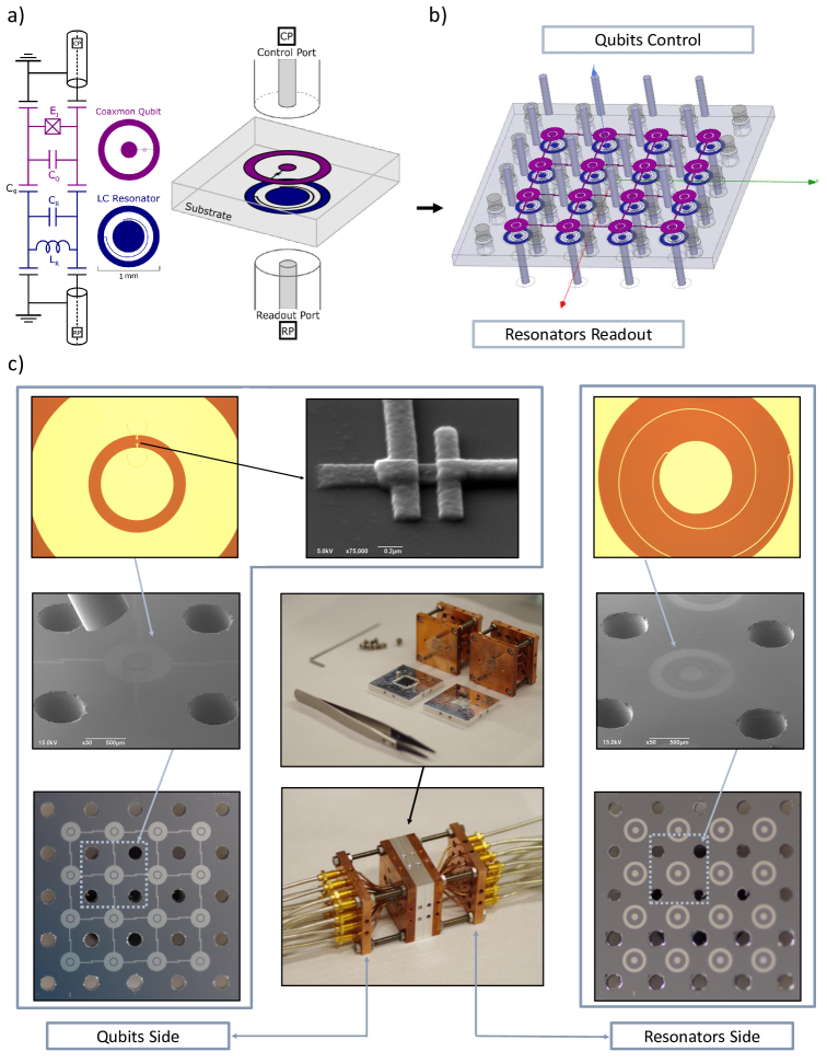
We demonstrate a scalable square lattice of 16 fixed-frequency transmon qubits, implemented in a 3D-integrated cQED architecture [62, 59, 60]. Each qubit is capacitively coupled through the substrate to a readout resonator positioned on the opposite side of the chip, featuring a tileable unit cell (see Fig. 1 (a)). This approach enables individual qubit control and readout in a compact lattice architecture (see Fig. 1 (b) and (c)). We implement off-chip inductive shunting on the device enclosure to mitigate box-mediated residual crosstalk originating from parasitic enclosure modes [59, 60]. Each qubit is capacitively coupled to its four nearest neighbors via lithographically patterned capacitive arms, facilitating interactions characterized by exchange energy rates in equ. 1 between each pair of qubits (see Fig. 3 (a)). See supplementary materials for more details on the fabrication process and experimental setup.
Basic Device Parameters
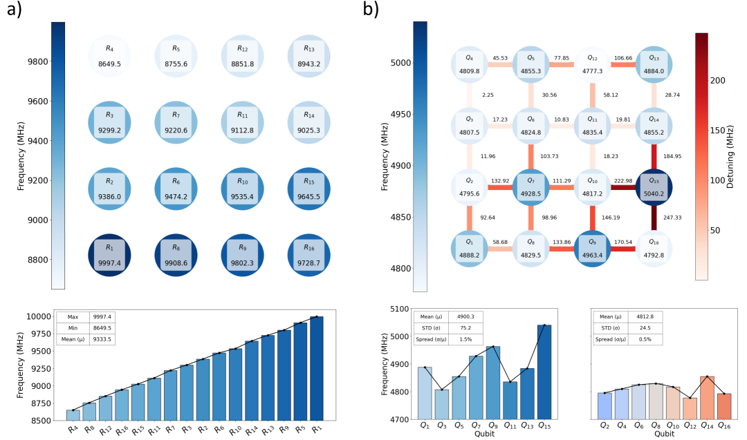
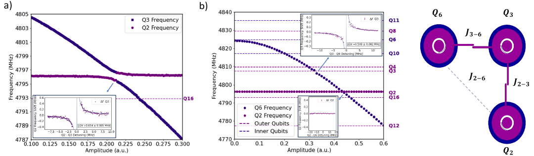
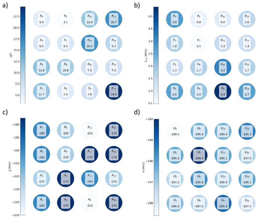
The resonators are designed to have distinct frequencies following a ladder design ranging from ~ 8.6 to 10.0 GHz, targeting well-separated readout frequencies (see Fig. 2(a)). Each set of 8 qubits is designed with two-distinct, alternating, frequency pattern in a range between 4.8 and 4.9 GHz, and measured with very low frequency spreads of and MHz, receptively, for both targeted values (see Fig. 2(b)). This frequency range allows operating in the straddling regime, where detunings of qubits remain smaller than their anharmonicities, necessary later for tuning up two-qubit interactions. We note that only two pairs of qubits, - and -, are outside the straddling regime due to a higher frequency of . The average anharmonicity is MHz across all qubits with a very low frequency spread of (see supplementary materials for more device parameters). The low frequency spreads were achieved without any further post-fabrication process on the junctions, such as junctions annealing [69], but only by fine tuning the junctions fabrication parameters.
Results and Discussion
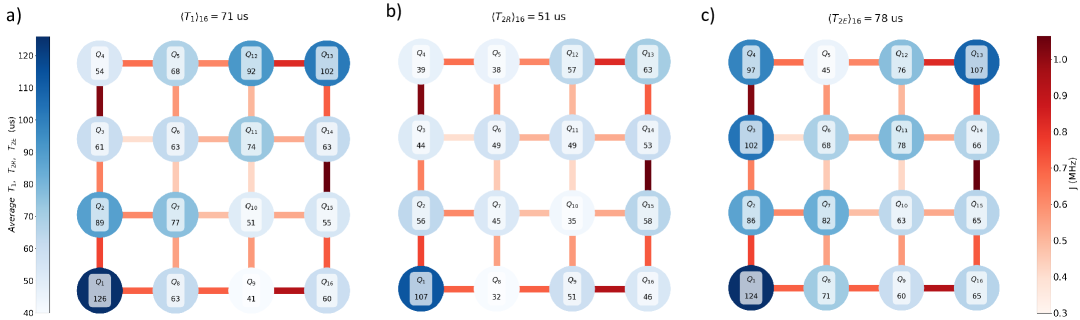
Qubits relaxation and coherence times were measured repeatedly over 12 hours, resulting in a total of 400 measurements for each , and that are then averaged for each qubit (see Fig. 3). The average qubits relaxation times are shown in Fig.3(a), and dephasing times and were measured using Ramsey and Hahn echo sequences and shown in Fig. 3(b) and Fig. 3(c), respectively. Relaxation and coherence times averaged across the lattice are , and , with weighted-standard deviations.
Crosstalk Characterization
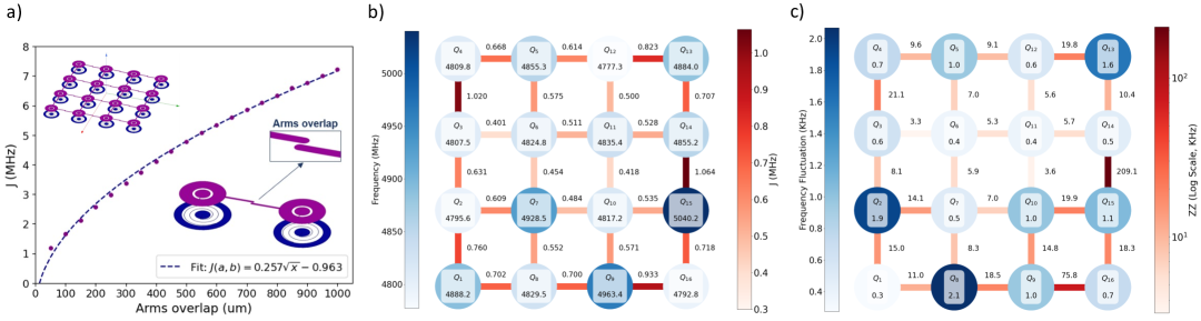
We present two methods to characterize direct coupling and crosstalk. One is based on ZZ measurements using equ. 3 and the second is based on direct measurements of anticrossing between different pairs of qubits using AC-Stark shift [70]. Fig. 4 shows both the design and measurements of the coupling between nearest-neighbor qubits. Fig. 4(a) shows how a simple impedance-based model [66] is used combined with HFSS simulations to model as a function of the capacitive arm overlap. In Fig. 4 (b) and (c), the measured ZZ shifts are used to calculate values across the device using equ. 3. The results also highlight each qubit’s frequency fluctuation, determined by ~ 400 repeated Ramsey measurements over ~ 12 hours, showing a very low frequency instability of about 0.88 KHz as an average of all frequency fluctuations across the device (see Fig. 4 (c)).
In particular, we observe low ZZ shifts across all qubit pairs except for two notable outliers occur for - (75.8 KHz) and - (209.1 KHz), which lie near higher transitions and near the edge of the straddling regime. The estimated couplings have maximum and minimum values at 1.064 MHz and 0.401 MHz, respectively. The mean of 0.623 MHz and standard deviation of 0.173 MHz lead to a relative spread of about 0.269 in different values of the coupling across the lattice.
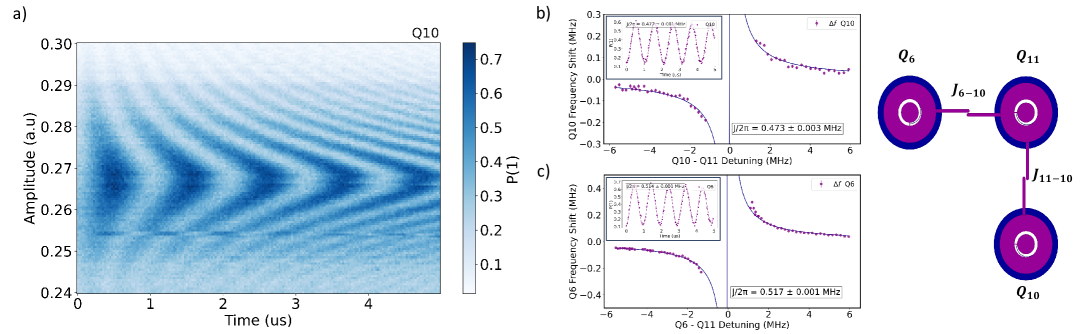
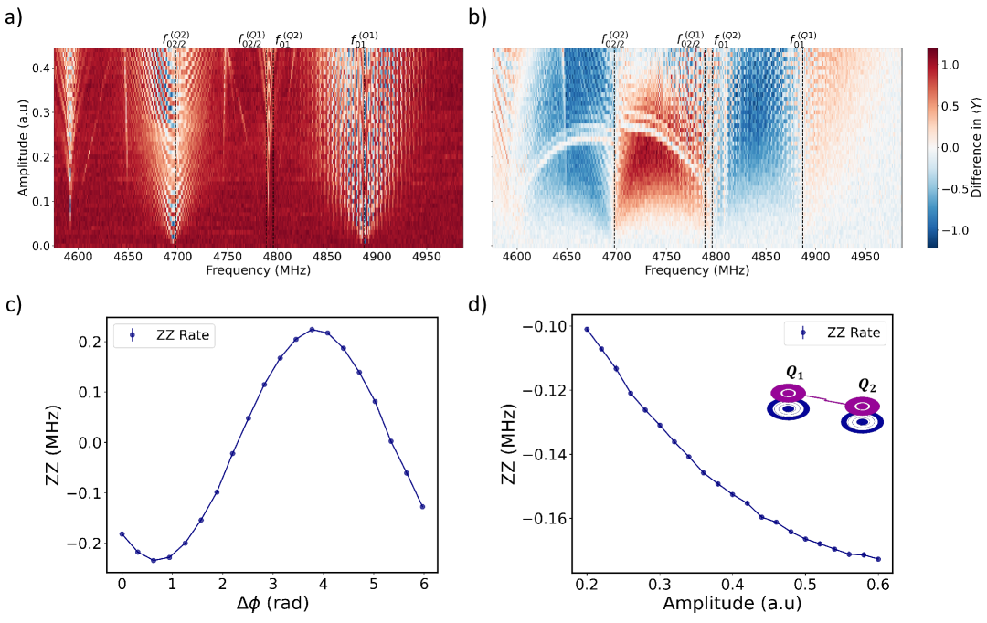
Next, direct measurements of anticrossing between different pairs of qubits using AC-Stark shift are shown in Fig. 5. This example illustrates both direct and indirect interactions in a simplified three-qubit setting in the lattice. In Fig. 5(a), one qubit is Stark-shifted until it is in resonance with its nearest neighbor, forming an avoided-crossing from which the exchange coupling is directly extracted by fitting to a simple model. Table 1 compares the resulting values for nearest neighbors obtained by performing AC-Stark shift Ramsey experiments, with those extracted from measuring static ZZ shifts, . We confirm these measurements by performing AC-Stark shift on another set of three qubit in lattice, and observe a swap of population between pairs of nearest-neighbor qubits (see Fig. 6(a)), and compare the exchange energy rates with those extracted from AC-Stark shift Ramsey measurements on the same pairs of qubits.
| Qubits | ||||||
|---|---|---|---|---|---|---|
| pair | MHz | MHz | MHz | MHz | MHz | MHz |
| 4795.6 | 4807.5 | 12.0 | 0.0081 | 0.631 | 0.654 | |
| 4807.5 | 4824.8 | 17.2 | 0.0033 | 0.401 | 0.508 | |
| 4824.8 | 4835.4 | 10.7 | 0.0053 | 0.511 | 0.517 | |
| 4835.4 | 4817.2 | 18.2 | 0.0036 | 0.418 | 0.473 | |
| 4835.4 | 4855.2 | 19.8 | 0.0057 | 0.528 | 0.536 |
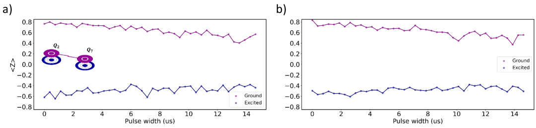
In addition, in Fig. 5(b), the same measurements are performed on diagonal pairs of qubits that are not directly connected by a capacitive arm, in which any measurable residual coupling represents crosstalk in this case. This long-range interaction arises from higher-order virtual processes or enclosure-mediated parasitic effects. In Fig. 5(b), we observe no long-range couplings across the lattice as one qubit is Stark-shifted across multiple adjacent qubits in frequency and space. The same observation is seen on multiple other cases summarized in Table 2. All measured values represents the frequency fluctuations from Ramsey as shown in the inset measurements in Fig. 5(b), which all remain significantly lower than the measured couplings for nearest neighbors, indicating that parasitic crosstalk is very small in the device. This supports the observation that the dominant couplings in the device are the deliberately engineered nearest-neighbor interactions and that spurious or long-range crosstalk can be kept well near the intrinsic frequency fluctuation levels of each qubit (see Fig. 4(c)).
| Qubits | Std-Dev | |||
|---|---|---|---|---|
| pair | MHz | MHz | MHz | MHz |
| 4795.6 | 4824.8 | 29.2 | 0.00507 | |
| 4824.8 | 4817.2 | 7.6 | 0.01200 | |
| 4855.1 | 4835.4 | 19.7 | 0.03927 | |
| 4829.5 | 4817.2 | 12.3 | 0.00807 | |
| 4817.2 | 4792.8 | 24.3 | 0.00662 |
Single-Qubit Gate Errors
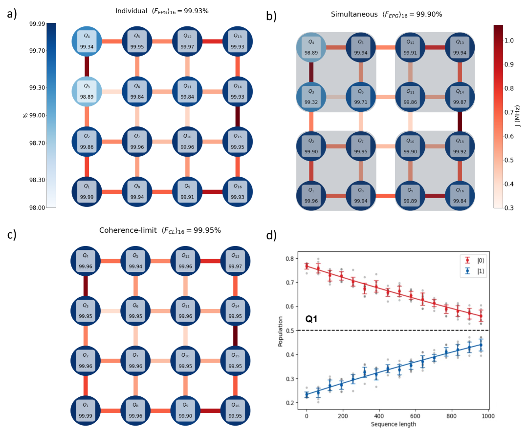
Single-qubit gate errors across the device are shown in Fig. 7, evaluated through randomized benchmarking (RB) [71, 72]. Fig.7(a) shows the error-per-physical-gate (EPG) values for individual qubits, while Fig. 7(b) shows simultaneous measurements on four-qubit sets across the lattice. RB experiments were conducted using an -Clifford decomposition for both individual and simultaneous gate errors. The resulting error rates were obtained by applying a combination of 60 ns duration (consisting of 50 ns Blackman envelope with 10 ns buffer) of , physical gates, combined with derivative removal gate (DRAG) pulse shaping [73] and virtual Z gates [74]. Single-shot readout was performed during all RB experiments with readout time of 8 us.
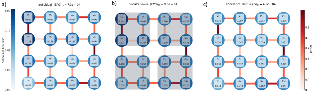
For both individual and simultaneous RB, each experiment was performed with 16 different Clifford sequences with total sequence length of 1000 gates and with each sequence repeated for distinct Clifford gates. Each of the 16 × 10 experiments was performed on every qubits for both individual and simultaneous RB (see supplementary materials). The EPG values obtained from these experiments are summarized Fig. 7(a) and (b). To compare the measured gate errors with coherent limits, the coherence-limited EPG (denoted as CLG) is shown in Fig. 7(c) and calculated using the expression [66], where is the total duration of each physical gate (60 ns), and and represent the relaxation and echo coherence times, respectively. This theoretical limit provides a benchmark to evaluate the fidelity of the single-qubit gates in relation to the intrinsic coherent errors. We observe very low median gate errors across the lattice and comparable EPGs on both individual and simultaneous RB experiments except for the pair of qubits - in which both qubits have higher errors due to the fact that this pair has very low detuning of 2.25 MHz (see Fig. 2(b)). Importantly, we observe comparable simultaneous (to individual) single-qubit gate errors across the lattice, despite the presence of always-on qubit-qubit coupling. This shows that correlated errors arising from residual crosstalk remain suppressed in the device, indicating minimal error propagation between qubits during simultaneous gates operations.
Two-Qubit Interactions and CZ Gates
We implement entangling operations between fixed-frequency transmon qubits in the lattice by using the Stark-induced ZZ by level excursions (siZZle) technique [75, 76] to boost static ZZ coupling. Here, we use two additional off-resonant drives to induce parametrized shifts in the energy levels of a two-transmons system as shown in Fig. 8(a). This approach modifies the native ZZ interaction and can be used to tune up a controlled-Z (CZ) gate by driving each transmon with a detuned microwave tone. The two simultaneous off-resonant drives on the two qubits shift the energy levels of the system and, through the capacitive coupling, modify the effective ZZ rate between the qubits. The modified ZZ rate can be approximated as [77]:
| (6) |
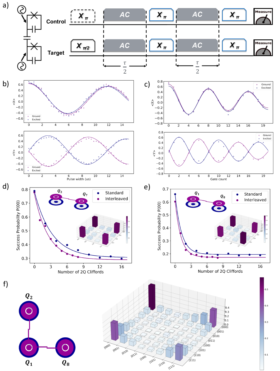
where denotes the static ZZ interaction rate in equ.3, and are the anharmonicities, is the fixed capacitive coupling strength, and , , , , and denote the drive amplitudes, detunings to each qubit, and relative phases of drives, respectively. In principle, the effective rate can be boosted or canceled depending on the sign of the additional driving term. The calibration of a CZ gate based on the siZZle interaction requires optimizing the drive parameters such that the total ZZ-induced phase accumulation during the gate operation equals . We set the two drive amplitudes to be relatively equal to , for maximum while observing a clean interaction, and here is the ratio between the amplitudes of the single-qubit pulses for the control to the target qubits. We have found this relation takes into account the asymmetries between the two drive amplitudes, introduced by cabling or room-temperature electronics. The relative phase between the two drives was found to be near-optimal in our setup and was set to be during CZ gate calibration. See supplementary materials for more details about tuning up two-qubit interactions and calibrating CZ gates.
Pulse sequence for siZZle gate calibration is shown in Fig. 8(a). The siZZle gate is implemented using two off-resonant Stark drives, with interleaved and final single-qubit pulses to cancel unwanted single-qubit phase accumulation. A dashed line on the the single-qubit pulse on the control in Fig. 8(a) denotes that the experiment is run both with and without exciting the control. In Fig. 8(b), pulse width Hamiltonian tomography on the target qubit is shown to extract the ZZ interaction. The duration of the Stark pulse here is swept while monitoring the phase evolution of the target qubit. In Fig. 8(c), repeated gate Hamiltonian tomography on the target qubit is shown. This experiment now uses fixed-duration two-qubit pulses and repetition blocks to more precisely calibrate the accumulated ZZ phase, which can then be used to implement an entangling gate. States of the control qubit during ZZ-induced phase accumulation on target qubit (see in Fig. 8(b)) are shown in Fig. 13 in supplementary materials.
We verified the calibrated CZ gate by interleaving it into a two-qubit randomized benchmarking (RB) sequence [78, 79], performed on multiple pairs across the lattice as shown in Fig. 8. The single-qubit gates here were optimally calibrated with 20 ns duration (consisting of 16 ns Blackman envelope with 4 ns buffer) of physical gates, combined with derivative removal gate (DRAG) pulse shaping [73] and virtual Z gates [74]. Single-shot readout was also optimized during all two-qubit experiments with a readout time of 3 us. The gate calibration consists of oberving ZZ-induced phase accumulation during the gate operation on the target qubits as shown in Fig. 8(b) and (c). The performance of the CZ gates was further complemented by the direct preparation of entangled Bell states between two qubits (in Fig. 8(d) and (e)), and preparation of GHZ state between three qubits across the lattice as shown in Fig. 8(f).
For the first pair in Fig. 8(d) consisting of (control) and (target), we achieve CZ gate fidelity of for a total gate time of , resulting in an average Bell state fidelity of measured by two-qubit state tomography. For the second pair in Fig. 8(e) consisting of (control) and (target), we achieve CZ gate fidelity of for a total gate time of , resulting in an average Bell state fidelity of measured by two-qubit state tomography. Finally, the prepared GHZ state between , and in Fig. 8(f) has an average GHZ state fidelity of measured by three-qubit state tomography.
Conclusion
We have demonstrated a scalable 4×4 square lattice of 16 fixed-frequency transmon qubits with nearest-neighbor capacitive coupling, implemented in a tileable, 3D-integrated cQED architecture with off-chip inductive shunting. The device achieves well-targeted qubit frequencies with very low spreads across two distinct frequency groups. We characterized coupling and crosstalk using both static ZZ shifts and direct anticrossing measurements, confirming that inter-qubit couplings remain localized, with negligible long-range parasitic interactions. Simultaneous randomized benchmarking shows low single-qubit gate errors and comparable to individual gate errors, with median error rates approaching coherence-limited errors. These results validate our design approach and present a practical architecture for scaling superconducting quantum circuits with low crosstalk and high qubit connectivity.
Acknowledgment
This work has received funding from the United Kingdom Engineering and Physical Sciences Research Council (EPSRC) under Grants No. EP/N015118/1, No. EP/T001062/1 and No. EP/W024772/1. M.B. acknowledges support from EPSRC QT Fellowship under Grant No. EP/W027992/1. S.C. acknowledges support from Schmidt Science. We would like to acknowledge the Superfab Nanofabrication facility at Royal Holloway, University of London, where part of device fabrication was performed.
Supplementary Materials
Superconducting quantum circuits are commonly fabricated using thin-films of aluminum, niobium, or titanium alloys on silicon or sapphire substrates [17]. The most critical components of these circuits are Josephson junctions, which when shunted with large capacitors, can form the widely used type of superconducting qubits known as the transmon [80]. The fabrication process of these junctions can vary based on the junction size controlled by electron-beam lithography exposure dose, oxidation parameters, and metal evaporation pressure. In our study, we employ a double-sided fabrication on a double-side 3-inch polished intrinsic silicon wafers, involving multiple lithography steps, thin-film depositions, and protective resists to ensure high-quality surfaces and interfaces on both sides during the fabrication process. The qubits and resonators are fabricated on opposite sides of the silicon substrate and capacitively coupled through the bulk substrate. The coupling strength is primarily determined by the substrate thickness and the geometry of the capacitive pads of both the qubit and the resonator [62].
Fabrication Process
The detailed steps of the fabrication process are described [18, 81, 79], with relevant design parameters given in Table 3. Spin-coating a protective photoresist layer on the backside is critical in double-sided fabrication process to protect the wafer and prevent additional contamination. The resonators side is patterned first while the qubit side is covered with photoresist, followed by cleaning the photoresist and spin-coating another protective photoresist layer on the resonators side and patterning the qubits side.
| Geometric parameter | Symbol | Standard value |
|---|---|---|
| Spiral line width | 5 µm | |
| Al thin film thickness | 100 nm | |
| JJ thin film thickness | (27-30) + 70 nm | |
| Si substrate thickness | 500 µm |
Wafer Cleaning
The fabrication process starts with cleaning a high-resistivity () intrinsic silicon wafer using a 10:1 buffered oxide etch (BOE) solution of hydrofluoric acid and ammonium fluoride to remove native oxides and contaminants. After etching, the wafers are thoroughly rinsed with ultrapure deionized water, dried with nitrogen gas, and promptly transferred (within 5 min) to minimize re-oxidation before thin-film deposition.
Aluminum Thin-Film Deposition
Immediately after water cleaning, the wafer is immediately loaded in Plassys MEB550S2 at ultra-high vacuum (UHV) and is baked up to for 10 min. After which a layer of 100 nm of aluminum is deposited at rate of 1 nm/s on the substrate through UHV electron-beam evaporation under controlled temperature and low-pressure conditions, with a base pressure down to mbar and an evaporation pressure of around mbar, ensuring high purity and uniformity of the thin film. The deposition rate and substrate temperature are carefully controlled to ensure smooth thin-film growth for optimal grain structure.
Photolithography and Micro-scale Circuit Elements
A positive photoresist AZ 1514 H is spin-coated onto the wafer and then exposed to ultraviolet light through a chrome photomask that defines the desired circuit patterns. After development with AZ 726 MIF developer solution, the exposed areas of aluminum are revealed for etching. The aluminum is then selectively etched away using a wet etching process to define the circuit elements. An aluminum etchant Alfa Aesar 44581 solution and water are used to achieve anisotropic etching with optimal selectivity to minimize remaining aluminum defects. This step creates the micro-scale features of the circuit, including capacitors, inductors, and coupling interconnects. Immediately after the etching process, residual resist is removed using DMSO.
Electron-Beam Lithography and Nano-scale Josephson Junctions
For the nano-scale features, high-resolution electron-beam lithography (EBL) is used to define the Josephson junctions. The junctions are fabricated using the Dolan bridge technique [82], which involves double-angle evaporation of aluminum to form the tunnel barriers, followed by careful removal of excess aluminum through a lift-off process. A bilayer resist structure is employed, consisting of a copolymer (MA/MMA) and a polymethyl methacrylate (PMMA) layer, to create an undercut profile necessary for the shadow evaporation process. After spin-coating the resist, EBL is carried out in a JEOL system at 100 keV, using aperture Ap4 size 2 nA - 60 for small features and Ap8 size 100 nA - 300 for large features, with doses typically around 1500 . Following the exposure, the critical features are then developed using a mixture of IPA/MIBK mixture in a 3:1 ratio.
After EBL patterning, the wafer is loaded into the Plassys MEB550S2. Prior to deposition, an argon (Ar) ion milling is performed for 1 min (voltage 400 V, acceleration voltage 90 V/s, current 15 mA) to remove any residual contaminants and native oxides from the metal and substrate surfaces, ensuring a clean interface for the subsequent aluminum deposition. The first layer of junction is then deposited at an angle of from normal incidence, depositing 60 nm of Al at a rate of 0.5 nm/s. Due to the deposition angle, the effective thickness of the deposited film is approximately 27-30 nm. Following the first deposition, an in situ controlled static oxidation inside Plassys is performed, typically for 5-10 min at an oxygen pressure of 5-10 mbar, depending on the target junction resistance. This controlled oxidation forms the thin insulating barrier of aluminum oxide essential for the tunnel junction. After pumping back down to UHV conditions, the second layer of aluminum is deposited at normal incidence (), depositing 70 nm of Al at a rate of 0.5 nm/s, effectively completing the Josephson junction structure. Precise control over the oxidation parameters, such as oxygen pressure and exposure time, is critical to achieve the desired tunnel barrier properties and, consequently, the critical current of the junction [82]. Following evaporation, a lift-off process is carried out in a DMSO solution at for around 2 hrs and immediately followed by thoroughly rinsing with ultrapure deionized water and drying using nitrogen gas.
Post-Fabrication Milling, Dicing and Packaging
The wafer is next spin-coated with a protective layer of AZ 1514 H photoresist on both sides to protect the surfaces during milling and dicing. For milling, a central aperture of 500 µm diameter is drilled with a diamond micro-grinding tool using a Loxham Precision µ6 micro-machining system. These micromachining steps require careful handling to avoid introducing contamination or mechanical damage on the wafer, which could lead to additional defects. After milling, the wafer is diced into individual square dies of approximately 10 mm side length using a Disco DAD3430 dicing saw. A diced chip is then mounted into a sample holder and prepared to be installed into a cryostat for microwave measurements.
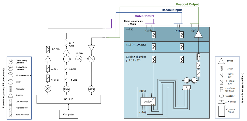
Experimental Setup
The experimental setup operates at a base temperature of using a dilution refrigerator. The control and readout of qubits are facilitated by the wiring configurations shown in Figure 9. For qubit control, microwave pulses are synthesized directly using QubiC system [83, 84]. The pulses are carefully shaped for single and two-qubit gates to align at the desired frequencies. For readout, reflected signals from the resonators go through amplification and down-conversion and are then captured by Analog-to-Digital Converters (ADCs) connected to the FPGA for measurements and further data analysis. The system is equipped with cryogenic attenuators and low-pass filters along the input lines to minimize thermal noise and spurious signals reaching the qubits. Output lines are similarly configured with isolators and cryogenic HEMT amplifiers to preserve signal integrity and maintain high signal-to-noise ratio throughout the measurement chain.
Additional Device Parameters
The following are the full datasets used to produce the results presented in the main text and more device parameters. Additional device parameters are visualized in Fig. 10 and given in Table. 4.
| Parameters | |||||||||
|---|---|---|---|---|---|---|---|---|---|
| Qubits | MHz | MHz | MHz | KHz | MHz | ||||
| 9997.4 | 4888.2 | 11.7 | 2.6 | -200.0 | -196.6 | 126 ± 18 | 107 ± 12 | 124 ± 23 | |
| 9386.0 | 4795.6 | 11.8 | 1.3 | -225.0 | -197.2 | 89 ± 13 | 56 ± 15 | 86 ± 12 | |
| 9299.2 | 4807.5 | 6.5 | 1.8 | -200.0 | -196.2 | 61 ± 6 | 44 ± 5 | 102 ± 18 | |
| 8649.5 | 4809.8 | 5.3 | 2.8 | -200.0 | -198.6 | 54 ± 9 | 39 ± 14 | 97 ± 20 | |
| 8755.6 | 4855.3 | 3.1 | 0.8 | -225.0 | -196.4 | 68 ± 10 | 38 ± 4 | 45 ± 10 | |
| 9220.6 | 4824.8 | 6.4 | 0.5 | -225.0 | -194.0 | 63 ± 7 | 49 ± 4 | 68 ± 10 | |
| 9474.2 | 4928.5 | 10.8 | 1.7 | -175.0 | -195.6 | 77 ± 12 | 45 ± 12 | 82 ± 15 | |
| 9908.6 | 4829.5 | 5.8 | 2.0 | -175.0 | -197.2 | 63 ± 8 | 32 ± 7 | 71 ± 8 | |
| 9802.3 | 4963.4 | 7.8 | 4.4 | -250.0 | -195.0 | 24 ± 7 | 24 ± 5 | 33 ± 9 | |
| 9535.4 | 4817.2 | 7.3 | 3.2 | -200.0 | -196.9 | 51 ± 10 | 35 ± 9 | 63 ± 17 | |
| 9112.8 | 4835.4 | 16.5 | 1.4 | -175.0 | -196.1 | 74 ± 7 | 49 ± 3 | 78 ± 13 | |
| 8851.8 | 4777.3 | 11.4 | 0.9 | -250.0 | -196.4 | 92 ± 24 | 57 ± 11 | 76 ± 15 | |
| 8943.2 | 4884.0 | 16.7 | 1.6 | -175.0 | -195.3 | 102 ± 13 | 63 ± 7 | 107 ± 22 | |
| 9025.3 | 4855.2 | 9.3 | 1.4 | -175.0 | -197.0 | 56 ± 12 | 56 ± 10 | 60 ± 15 | |
| 9645.5 | 5040.2 | 7.3 | 1.7 | -225.0 | -196.1 | 55 ± 7 | 58 ± 9 | 65 ± 9 | |
| 9728.7 | 4792.8 | 24.6 | 2.7 | -175.0 | -197.5 | 60 ± 6 | 46 ± 4 | 65 ± 9 | |
| Statistics | |||||||||
| Max | 9997.4 | 5040.2 | 24.6 | 4.4 | -175.0 | -194.0 | 126 | 107 | 124 |
| Min | 8649.5 | 4777.3 | 3.1 | 0.5 | -250.0 | -198.6 | 41 | 32 | 45 |
| (Mean) | 9333.5 | 4856.5 | 10.1 | 1.9 | -203.1 | -196.4 | 71 | 51 | 78 |
| (Std. Dev) | 407.12 | - | 5.3 | 0.96 | 26.3 | 1.1 | 21 | 17 | 20 |
| () | 101.8 | - | 1.3 | 0.2 | 6.6 | 0.3 | 5 | 4 | 5 |
Single-Qubit Gate Calibration
Randomized benchmarking (RB) [71, 72] experiments were conducted using an -Clifford decomposition for both individual and simultaneous four-qubits gate fidelities. Detailed single-qubit gate fidelities are given in Table. 5 and Table. 6, and shown in Fig.11 with an example of RB measured trace on shown in in Fig.11(d).
| Parameters | EPC | EPC Error | EPG | EPG Error | CLG | CLG Error | |||
|---|---|---|---|---|---|---|---|---|---|
| Qubits | Error per Clifford Gate | Error | % | Error per Physical Gate | Error | % | Coh. Lim. Error per Gate | Error | % |
| 1.212E-04 | 1.167E-04 | 99.988 | 6.640E-05 | 6.393E-05 | 99.993 | 1.111E-04 | 1.730E-05 | 99.989 | |
| 2.531E-03 | 2.520E-04 | 99.747 | 1.388E-03 | 1.381E-04 | 99.861 | 3.689E-04 | 5.286E-05 | 99.963 | |
| 2.014E-02 | 1.237E-02 | 97.986 | 1.108E-02 | 6.780E-03 | 98.892 | 5.375E-04 | 6.706E-05 | 99.946 | |
| 1.205E-02 | 2.777E-03 | 98.795 | 6.622E-03 | 1.522E-03 | 99.338 | 3.915E-04 | 5.258E-05 | 99.961 | |
| 8.595E-04 | 7.357E-05 | 99.914 | 4.711E-04 | 4.031E-05 | 99.953 | 5.919E-04 | 1.012E-04 | 99.941 | |
| 2.852E-03 | 2.096E-04 | 99.715 | 1.564E-03 | 1.148E-04 | 99.844 | 4.672E-04 | 4.662E-05 | 99.953 | |
| 6.773E-04 | 1.818E-04 | 99.932 | 3.712E-04 | 9.961E-05 | 99.963 | 3.739E-04 | 4.903E-05 | 99.963 | |
| 1.027E-03 | 6.242E-05 | 99.897 | 5.630E-04 | 3.420E-05 | 99.944 | 4.406E-04 | 3.763E-05 | 99.956 | |
| 1.591E-03 | 8.031E-05 | 99.841 | 8.719E-04 | 4.400E-05 | 99.913 | 1.024E-03 | 2.056E-04 | 99.898 | |
| 6.621E-04 | 1.169E-04 | 99.934 | 3.629E-04 | 6.406E-05 | 99.964 | 5.138E-04 | 9.399E-05 | 99.949 | |
| 2.821E-03 | 2.885E-04 | 99.718 | 1.547E-03 | 1.581E-04 | 99.845 | 3.917E-04 | 4.464E-05 | 99.961 | |
| 6.173E-04 | 9.181E-05 | 99.938 | 3.383E-04 | 5.031E-05 | 99.966 | 3.720E-04 | 5.922E-05 | 99.963 | |
| 1.299E-03 | 1.224E-04 | 99.870 | 7.122E-04 | 6.706E-05 | 99.929 | 2.850E-04 | 4.043E-05 | 99.971 | |
| 1.355E-03 | 8.207E-05 | 99.865 | 7.426E-04 | 4.497E-05 | 99.926 | 5.122E-04 | 9.179E-05 | 99.949 | |
| 9.704E-04 | 7.331E-05 | 99.903 | 5.318E-04 | 4.017E-05 | 99.947 | 4.898E-04 | 4.853E-05 | 99.951 | |
| 1.353E-03 | 1.367E-04 | 99.865 | 7.419E-04 | 7.490E-05 | 99.926 | 4.746E-04 | 4.579E-05 | 99.953 |
| Parameters | EPC | EPC Error | EPG | EPG Error | CLG | CLG Error | |||
|---|---|---|---|---|---|---|---|---|---|
| Qubits | Error per Clifford Gate | Error | % | Error per Physical Gate | Error | % | Coh. Lim. Error per Gate | Error | % |
| 7.152E-04 | 1.149E-04 | 99.928 | 3.919E-04 | 6.299E-05 | 99.961 | 1.111E-04 | 1.730E-05 | 99.989 | |
| 1.782E-03 | 3.456E-04 | 99.822 | 9.768E-04 | 1.894E-04 | 99.902 | 3.689E-04 | 5.286E-05 | 99.963 | |
| 1.233E-02 | 2.312E-03 | 98.767 | 6.775E-03 | 1.267E-03 | 99.323 | 5.375E-04 | 6.706E-05 | 99.946 | |
| 2.024E-02 | 7.128E-03 | 97.976 | 1.114E-02 | 3.906E-03 | 98.886 | 3.915E-04 | 5.258E-05 | 99.961 | |
| 1.137E-03 | 7.717E-05 | 99.886 | 6.232E-04 | 4.228E-05 | 99.938 | 5.919E-04 | 1.012E-04 | 99.941 | |
| 5.231E-03 | 6.081E-04 | 99.477 | 2.870E-03 | 3.332E-04 | 99.713 | 4.672E-04 | 4.662E-05 | 99.953 | |
| 9.912E-04 | 1.300E-04 | 99.901 | 5.432E-04 | 7.122E-05 | 99.946 | 3.739E-04 | 4.903E-05 | 99.963 | |
| 1.170E-03 | 1.065E-04 | 99.883 | 6.412E-04 | 5.836E-05 | 99.936 | 4.406E-04 | 3.763E-05 | 99.956 | |
| 1.909E-03 | 1.267E-04 | 99.809 | 1.047E-03 | 6.943E-05 | 99.895 | 1.024E-03 | 2.056E-04 | 99.898 | |
| 1.802E-03 | 2.894E-04 | 99.820 | 9.879E-04 | 1.586E-04 | 99.901 | 5.138E-04 | 9.399E-05 | 99.949 | |
| 2.529E-03 | 1.516E-04 | 99.747 | 1.387E-03 | 8.307E-05 | 99.861 | 3.917E-04 | 4.464E-05 | 99.961 | |
| 1.565E-03 | 1.710E-04 | 99.844 | 8.578E-04 | 9.369E-05 | 99.914 | 3.720E-04 | 5.922E-05 | 99.963 | |
| 1.003E-03 | 9.206E-05 | 99.900 | 5.499E-04 | 5.044E-05 | 99.945 | 2.850E-04 | 4.043E-05 | 99.971 | |
| 2.383E-03 | 1.273E-04 | 99.762 | 1.307E-03 | 6.974E-05 | 99.869 | 5.122E-04 | 9.179E-05 | 99.949 | |
| 1.451E-03 | 9.408E-05 | 99.855 | 7.955E-04 | 5.155E-05 | 99.920 | 4.898E-04 | 4.853E-05 | 99.951 | |
| 2.848E-03 | 3.135E-04 | 99.715 | 1.561E-03 | 1.718E-04 | 99.844 | 4.746E-04 | 4.579E-05 | 99.953 |
Two-Qubit Interaction and Gate Calibration
The calibration of a CZ gate based on the siZZle interaction, it requires optimizing the drive parameters such that the total ZZ-induced phase accumulation during the gate operation equals . This involves first tuning up the frequencies of the off-resonant drives to achieve optimal detunings and from the qubits’ transitions, selecting both optimal amplitudes ( and ) and phase difference ( between the off-resonant drives to maximize the rate, and finally working the gate duration out of the optimal rate.
The calibration procedure begins by selecting an initial set of Stark drive parameters. Specifically, a drive frequency and amplitude are first selected to observe an initail ZZ interctaion. This assessment is carried out using Hamiltonian tomography followed by repeated gate tomography, as illustrated in Fig. 8(b) and (c), respectively. Non-optimal parameters typically lead to unstable or noisy oscillations in the expectation values. In such cases, the parameters are iteratively adjusted until clean, stable oscillations are observed. Once stability is achieved, an automated fitting routine is used to extract the optimal gate duration to proceed to the calibration of a CZ entangling gate.
To tune the ZZ interaction more precisely, we perform a two-dimensional parameter sweep over the Stark drive frequency and amplitude shown in Fig. 12, building a coarse map of the ZZ interaction rates. Although directly measuring the ZZ rate at every point would be ideal, it is experimentally very expensive. Instead, we fix the Stark pulse duration at s and use the Hamiltonian tomography sequence in Fig. 8(b), recording the differential phase accumulation on the target qubit on basis when the control qubit is initialized in either the ground or excited state. This entire mapping procedure takes roughly 12 hours and yields the background for the interaction landscape over a wide range of parameters. Following this, we analyze both the control qubit (in Fig. 12(a)) and target qubit (in Fig. 12(b)) dynamics to identify the optimal parameters for high-contrast, coherent interactions.
References
- [1] Kim, Y. et al. Evidence for the utility of quantum computing before fault tolerance. \JournalTitleNature 618, 500–505 (2023).
- [2] Preskill, J. Quantum computing 40 years later. In Feynman Lectures on Computation, 193–244 (CRC Press, 2023).
- [3] Shor, P. W. Scheme for reducing decoherence in quantum computer memory. \JournalTitlePhysical review A 52, R2493 (1995).
- [4] Gottesman, D. Stabilizer codes and quantum error correction (California Institute of Technology, 1997).
- [5] Putterman, H. et al. Hardware-efficient quantum error correction using concatenated bosonic qubits. \JournalTitlearXiv preprint arXiv:2409.13025 (2024).
- [6] Brock, B. L. et al. Quantum error correction of qudits beyond break-even. \JournalTitlearXiv preprint arXiv:2409.15065 (2024).
- [7] Lacroix, N. et al. Scaling and logic in the color code on a superconducting quantum processor. \JournalTitlearXiv preprint arXiv:2412.14256 (2024).
- [8] Acharya, R. et al. Quantum error correction below the surface code threshold. \JournalTitlearXiv preprint arXiv:2408.13687 (2024).
- [9] Eickbusch, A. et al. Demonstrating dynamic surface codes. \JournalTitlearXiv preprint arXiv:2412.14360 (2024).
- [10] Karamlou, A. H. et al. Probing entanglement in a 2D hard-core Bose-Hubbard lattice. \JournalTitleNature 1–6 (2024).
- [11] Rosenberg, E. et al. Dynamics of magnetization at infinite temperature in a heisenberg spin chain. \JournalTitleScience 384, 48–53 (2024).
- [12] Cochran, T. A. et al. Visualizing dynamics of charges and strings in (2+ 1) d lattice gauge theories. \JournalTitlearXiv preprint arXiv:2409.17142 (2024).
- [13] Gyawali, G. et al. Observation of disorder-free localization and efficient disorder averaging on a quantum processor. \JournalTitlearXiv preprint arXiv:2410.06557 (2024).
- [14] Measurement-induced entanglement and teleportation on a noisy quantum processor. \JournalTitleNature 622, 481–486 (2023).
- [15] Malz, D. & Smith, A. Topological two-dimensional Floquet lattice on a single superconducting qubit. \JournalTitlePhysical Review Letters 126, 163602 (2021).
- [16] Daley, A. J. et al. Practical quantum advantage in quantum simulation. \JournalTitleNature 607, 667–676 (2022).
- [17] Siddiqi, I. Engineering high-coherence superconducting qubits. \JournalTitleNature Reviews Materials 6, 875–891 (2021).
- [18] Alghadeer, M. et al. Characterization of nanostructural imperfections in superconducting quantum circuits. \JournalTitlearXiv preprint arXiv:2501.15059 (2025).
- [19] Alghadeer, M. et al. Mitigating coherent loss in superconducting circuits using molecular self-assembled monolayers. \JournalTitleScientific Reports 14, 27340 (2024).
- [20] Alghadeer, M. et al. Surface passivation of niobium superconducting quantum circuits using self-assembled monolayers. \JournalTitleACS Applied Materials & Interfaces 15, 2319–2328 (2022).
- [21] Chistolini, T. et al. Performance of Superconducting Resonators Suspended on SiN Membranes. \JournalTitlearXiv preprint arXiv:2405.01784 (2024).
- [22] Altoé, M. V. P. et al. Localization and mitigation of loss in niobium superconducting circuits. \JournalTitlePRX Quantum 3, 020312 (2022).
- [23] Bakr, M. et al. Multiplexed Readout of Superconducting Qubits Using a 3D Re-entrant Cavity Filter. \JournalTitlearXiv preprint arXiv:2412.14853 (2024).
- [24] Bakr, M. Dynamic josephson junction metasurfaces for multiplexed control of superconducting qubits. \JournalTitlearXiv preprint arXiv:2411.01345 (2024).
- [25] Fasciati, S. D. et al. Complementing the transmon by integrating a geometric shunt inductor. \JournalTitlearXiv preprint arXiv:2410.10416 (2024).
- [26] Mohseni, M. et al. How to build a quantum supercomputer: Scaling challenges and opportunities. \JournalTitlearXiv preprint arXiv:2411.10406 (2024).
- [27] Zanuz, D. C. et al. Mitigating losses of superconducting qubits strongly coupled to defect modes. \JournalTitlearXiv preprint arXiv:2407.18746 (2024).
- [28] Abdurakhimov, L. V. et al. Identification of different types of high-frequency defects in superconducting qubits. \JournalTitlePRX Quantum 3, 040332 (2022).
- [29] Bilmes, A. et al. Resolving the positions of defects in superconducting quantum bits. \JournalTitleScientific reports 10, 3090 (2020).
- [30] Krinner, S. et al. Engineering cryogenic setups for 100-qubit scale superconducting circuit systems. \JournalTitleEPJ Quantum Technology 6, 2 (2019).
- [31] Le, N. H., Cykiert, M. & Ginossar, E. Scalable and robust quantum computing on qubit arrays with fixed coupling. \JournalTitlenpj Quantum Information 9, 1 (2023).
- [32] Koch, J. et al. Charge-insensitive qubit design derived from the cooper pair box. \JournalTitlePhysical Review A Atomic, Molecular, and Optical Physics 76, 042319 (2007).
- [33] Place, A. P. et al. New material platform for superconducting transmon qubits with coherence times exceeding 0.3 milliseconds. \JournalTitleNature communications 12, 1779 (2021).
- [34] Yan, F. et al. Tunable coupling scheme for implementing high-fidelity two-qubit gates. \JournalTitlePhysical Review Applied 10, 054062 (2018).
- [35] Ketterer, A. & Wellens, T. Characterizing crosstalk of superconducting transmon processors. \JournalTitlePhysical Review Applied 20, 034065 (2023).
- [36] Tripathi, V. et al. Suppression of crosstalk in superconducting qubits using dynamical decoupling. \JournalTitlePhysical Review Applied 18, 024068 (2022).
- [37] Murali, P., McKay, D. C., Martonosi, M. & Javadi-Abhari, A. Software mitigation of crosstalk on noisy intermediate-scale quantum computers. In Proceedings of the Twenty-Fifth International Conference on Architectural Support for Programming Languages and Operating Systems, 1001–1016 (2020).
- [38] Krinner, S. et al. Benchmarking coherent errors in controlled-phase gates due to spectator qubits. \JournalTitlePhysical Review Applied 14, 024042 (2020).
- [39] Zhao, P. et al. Quantum crosstalk analysis for simultaneous gate operations on superconducting qubits. \JournalTitlePRX quantum 3, 020301 (2022).
- [40] Fors, S. P., Fernández-Pendás, J. & Kockum, A. F. Comprehensive explanation of ZZ coupling in superconducting qubits. \JournalTitlearXiv preprint arXiv:2408.15402 (2024).
- [41] Chow, J. M. et al. Simple all-microwave entangling gate for fixed-frequency superconducting qubits. \JournalTitlePhysical review letters 107, 080502 (2011).
- [42] Chow, J. M. et al. Microwave-activated conditional-phase gate for superconducting qubits. \JournalTitleNew Journal of Physics 15, 115012 (2013).
- [43] Xu, Y. et al. High-fidelity, high-scalability two-qubit gate scheme for superconducting qubits. \JournalTitlePhysical review letters 125, 240503 (2020).
- [44] Wei, K. et al. Hamiltonian engineering with multicolor drives for fast entangling gates and quantum crosstalk cancellation. \JournalTitlePhysical Review Letters 129, 060501 (2022).
- [45] Xu, Y. et al. High-fidelity, high-scalability two-qubit gate scheme for superconducting qubits. \JournalTitlePhysical review letters 125, 240503 (2020).
- [46] Collodo, M. C. et al. Implementation of conditional phase gates based on tunable zz interactions. \JournalTitlePhysical review letters 125, 240502 (2020).
- [47] Sung, Y. et al. Realization of high-fidelity CZ and ZZ-free iSWAP gates with a tunable coupler. \JournalTitlePhysical Review X 11, 021058 (2021).
- [48] Stehlik, J. et al. Tunable coupling architecture for fixed-frequency transmon superconducting qubits. \JournalTitlePhysical review letters 127, 080505 (2021).
- [49] Long, J. et al. A universal quantum gate set for transmon qubits with strong ZZ interactions. \JournalTitlearXiv preprint arXiv:2103.12305 (2021).
- [50] Chu, J. & Yan, F. Coupler-assisted controlled-phase gate with enhanced adiabaticity. \JournalTitlePhysical Review Applied 16, 054020 (2021).
- [51] Chen, Y. et al. Voltage-activated parametric entangling gates based on gatemon qubits. \JournalTitlePhysical Review Applied 20, 044012 (2023).
- [52] Ganzhorn, M. et al. Benchmarking the noise sensitivity of different parametric two-qubit gates in a single superconducting quantum computing platform. \JournalTitlePhysical Review Research 2, 033447 (2020).
- [53] McKay, D. C., Sheldon, S., Smolin, J. A., Chow, J. M. & Gambetta, J. M. Three-qubit randomized benchmarking. \JournalTitlePhysical review letters 122, 200502 (2019).
- [54] Bharti, K. et al. Noisy intermediate-scale quantum algorithms. \JournalTitleReviews of Modern Physics 94, 015004 (2022).
- [55] Megrant, A. & Chen, Y. Scaling up superconducting quantum computers. \JournalTitleNature Electronics 1–3 (2025).
- [56] Kosen, S. et al. Signal crosstalk in a flip-chip quantum processor. \JournalTitlePRX Quantum 5, 030350 (2024).
- [57] Das, R. N. et al. Reworkable superconducting qubit package for quantum computing. In 2024 IEEE 74th Electronic Components and Technology Conference (ECTC), 427–432 (IEEE, 2024).
- [58] Huang, S. et al. Microwave package design for superconducting quantum processors. \JournalTitlePRX Quantum 2, 020306 (2021).
- [59] Spring, P., Tsunoda, T., Vlastakis, B. & Leek, P. Modeling enclosures for large-scale superconducting quantum circuits. \JournalTitlePhysical Review Applied 14, 024061 (2020).
- [60] Spring, P. A. et al. High coherence and low cross-talk in a tileable 3D integrated superconducting circuit architecture. \JournalTitleScience Advances 8, eabl6698 (2022).
- [61] Krasnok, A. et al. Superconducting microwave cavities and qubits for quantum information systems. \JournalTitleApplied Physics Reviews 11 (2024).
- [62] Rahamim, J. et al. Double-sided coaxial circuit qed with out-of-plane wiring. \JournalTitleApplied Physics Letters 110 (2017).
- [63] DiCarlo, L. et al. Demonstration of two-qubit algorithms with a superconducting quantum processor. \JournalTitleNature 460, 240–244 (2009).
- [64] Chow, J. M. et al. Microwave-activated conditional-phase gate for superconducting qubits. \JournalTitleNew Journal of Physics 15, 115012 (2013).
- [65] Magesan, E. & Gambetta, J. M. Effective hamiltonian models of the cross-resonance gate. \JournalTitlePhysical Review A 101, 052308 (2020).
- [66] Solgun, F., DiVincenzo, D. P. & Gambetta, J. M. Simple impedance response formulas for the dispersive interaction rates in the effective hamiltonians of low anharmonicity superconducting qubits. \JournalTitleIEEE transactions on microwave theory and techniques 67, 928–948 (2019).
- [67] Solgun, F. & Srinivasan, S. Direct calculation of ZZ interaction rates in multimode circuit quantum electrodynamics. \JournalTitlePhysical Review Applied 18, 044025 (2022).
- [68] Blais, A., Grimsmo, A. L., Girvin, S. M. & Wallraff, A. Circuit quantum electrodynamics. \JournalTitleReviews of Modern Physics 93, 025005 (2021).
- [69] Hertzberg, J. B. et al. Laser-annealing josephson junctions for yielding scaled-up superconducting quantum processors. \JournalTitlenpj Quantum Information 7, 129 (2021).
- [70] Wallraff, A. et al. Sideband transitions and two-tone spectroscopy of a superconducting qubit strongly coupled to an on-chip cavity. \JournalTitlePhysical Review Letters 99, 050501 (2007).
- [71] Chow, J. et al. Randomized benchmarking and process tomography for gate errors in a solid-state qubit. \JournalTitlePhysical review letters 102, 090502 (2009).
- [72] Gambetta, J. M. et al. Characterization of addressability by simultaneous randomized benchmarking. \JournalTitlePhysical review letters 109, 240504 (2012).
- [73] Motzoi, F., Gambetta, J. M., Rebentrost, P. & Wilhelm, F. K. Simple pulses for elimination of leakage in weakly nonlinear qubits. \JournalTitlePhysical review letters 103, 110501 (2009).
- [74] McKay, D. C., Wood, C. J., Sheldon, S., Chow, J. M. & Gambetta, J. M. Efficient z gates for quantum computing. \JournalTitlePhysical Review A 96, 022330 (2017).
- [75] Mitchell, B. K. et al. Hardware-efficient microwave-activated tunable coupling between superconducting qubits. \JournalTitlePhys. Rev. Lett. 127, 200502, DOI: 10.1103/PhysRevLett.127.200502 (2021).
- [76] Wei, K. X. et al. Hamiltonian engineering with multicolor drives for fast entangling gates and quantum crosstalk cancellation. \JournalTitlePhys. Rev. Lett. 129, 060501, DOI: 10.1103/PhysRevLett.129.060501 (2022).
- [77] Wei, K. et al. Quantum crosstalk cancellation for fast entangling gates and improved multi-qubit performance. \JournalTitlearXiv preprint arXiv:2106.00675 (2021).
- [78] Cao, S. et al. Emulating two qubits with a four-level transmon qudit for variational quantum algorithms. \JournalTitlearXiv preprint arXiv:2303.04796 (2023).
- [79] Cao, S. Implementation of variational quantum algorithms on superconducting qudits. Ph.D. thesis, University of Oxford (2023).
- [80] Koch, J. et al. Charge-insensitive qubit design derived from the cooper pair box. \JournalTitlePhysical Review A 76, 042319 (2007).
- [81] Peterer, M. Experiments on multi-level superconducting qubits and coaxial circuit QED. Ph.D. thesis, University of Oxford (2016).
- [82] Dolan, G. & Dunsmuir, J. Very small ( 20 nm) lithographic wires, dots, rings, and tunnel junctions. \JournalTitlePhysica B: Condensed Matter 152, 7–13 (1988).
- [83] Xu, Y. et al. Qubic: An open-source fpga-based control and measurement system for superconducting quantum information processors. \JournalTitleIEEE Transactions on Quantum Engineering 2, 1–11 (2021).
- [84] Huang, G. et al. Qubic 2.0: A flexible advanced full stack quantum bit control system. In 2023 IEEE International Conference on Quantum Computing and Engineering (QCE), vol. 2, 248–249 (IEEE, 2023).