Electron and positron channeling and photon emission processes in boron doped periodically bent diamond
Abstract
In this paper, theoretical and numerical analyses are conducted of the profiles of the planar (-110) crystallographic direction in the diamond layer doped with boron atoms. The planar profiles for periodic doping following several ideal dependencies of the boron concentration on the distance in the crystalline medium. Numerical simulations of the channeling and photon emission processes have been carried out for 855 MeV electron and 530 MeV positron beams incident on boron-doped diamond with a four-period bending profile in the samples grown at the European Synchrotron Radiation Facility (ESRF). The simulations were performed using the MBN Explorer software package. It is shown that the channeling efficiency and the intensity of the crystalline undulator radiation strongly depend on the orientation of the incident beam relative to the bent channel profile at the entrance to the boron-doped layer. For the same conditions at the crystal entrance, the intestity of radiation emitted by positrons is significantly higher than that for electrons.
I Introduction
The interaction of high-energy charged particles with crystals is sensitive to the incoming beam direction relative to the target’s major crystallographic directions. Projectiles, impacting upon a crystal at small angles to its planes (or axes) can propagate large distances in the crystalline media following the planar (axial) direction. This specific motion, termed channeling motion, is due to the collective action of the electrostatic fields of the lattice atoms [1]. Research into the channeling process of ultra-relativistic projectiles in oriented crystals has emerged as a broad field [3, 2, 4, 5] with applications encompassing beam steering [6], collimation [7], focusing [8] and extraction [9].
Oriented crystals of different geometries irradiated by beams of ultra-relativistic electrons and positrons can potentially serve as novel crystal-based light sources (CLS) that produce intense gamma-ray radiation in the MeV-GeV photon energy range [5, 10, 11]. As demonstrated recently [13], the photon fluxes generated in such systems can exceed the levels achievable at modern laser-Compton gamma-ray light sources. The practical realization of CLSs is the subject of the ongoing Horizon Europe EIC-Pathfinder-2021 project TECHNO-CLS [12].
One of the proposed schemes for the implementation of CLSs employs crystalline undulators (CU), wherein the radiation is emitted by ultra-relativistic electrons or positrons channeling in a periodically bent crystal [14, 15, 16, 4]. In such systems, in addition to the channeling radiation [17], the CU radiation (CUR) is emitted due to the periodicity of the trajectory of a particle following the bending profile [14, 15]. PBCs are advantageous because the characteristics of the emitted radiation can be optimised for given parameters of the incident beam by varying the amplitude and the period of the bending. However, the operating efficiency of such a device depends on the quality of periodic bending [4]. The fabrication of PBCs, which are typically made of materials such as silicon, germanium, or diamond, poses a significant technological challenge. In order to achieve the periodical deformation of the crystalline structure, several techniques have been developed. These include mechanical scratching [18], laser ablation technique [19], the grooving method [20, 21], tensile/compressive strips deposition [22, 23, 24], sandblasting [25], ion implantation [26], and ultrasonic waves [14, 27, 28, 29].
Another approach to achieving periodic bending in crystals was proposed [30, 31, 32], which involves the introduction of dopant atoms to the crystalline structure. This method enables the reduction of the bending period to a range of a few microns. The fabrication of doped crystals can be achieved through a variety of methods, with each technique suited to growing different types of crystals. In the case of CLSs, particular attention has been focused on two crystal types: Silicon crystals doped with Germanium (Si1-x Gex), grown through molecular beam epitaxy [33], and Diamond crystals doped with Boron (C1-x Bx), grown via chemical vapour deposition (CVD) [34]. Here, denotes the dopant relative concentration. The boron-doped diamond layer cannot be separated from a single diamond substrate on which the superlattice is synthesised. Therefore, unlike Si1-x Gex superlattice, a diamond-based superlattice essentially has a heterocrystal structure, i.e., it consists of two segments: a straight single-crystal diamond substrate and a periodically doped layer.
In recent years, several channeling experiments have been carried out with periodically bent doped crystals to detect CUR [37, 35, 36, 38, 39, 40, 41] but no clear CUR signal was detected. The first observation of the CUR peak has been reported very recently [42] for a 855 MeV electron beam channeling in a periodically bent oriented diamond(110) crystal. We note that the existance of this peak, its position and intensity were predicted earlier in Refs. [43, 44].
In this paper we carry out theoretical analysis of the profile of periodically bent planes in the diamond layer doped periodically with boron atoms. It is demonstrated that it is essential to know the precise orientation of the undulator axis relative to the crystallographic directions in the substrate. This knowledge is needed to determine (i) the optimal direction of the incident beam, and (ii) the position of a detector to register the emitted radiation. The most intense undulator radiation is emitted in the cone along the undulator axis (where is the Lorentz factor of the ultra-relativistic charged particle). Therefore, to maximise the collection of the radiation the detector must be placed on the axis. This is particularly important if the detector aperture is smaller than the natural emission cone . The results of numerical simulations of the radiation emitted by ultra-relativistic electrons and positrons presented in Section III support this statement.
The simulations of the particles passage in a crystalline media and of the photon emission process have been performed using the MBN Explorer software package [47] for advanced multi-scale modelling of complex molecular structures and dynamics. MBN Studio [46], a multi-task toolkit and a dedicated graphical user interface for MBN Explorer, was used to construct the systems, prepare input files, and analyse simulation outputs. A special module of the package [45] allows the simulation of the passage of various particles (positively and negatively charged, light and heavy) through a variety of media, including single, bent and periodically bent crystals, hetero-crystalline structures (such as superlattices), and many others. The software simulates the trajectories within the framework of classical Relativistic Molecular Dynamics (RelMD). The dedicated computational algorithms allow the simulations of particle dynamics at macroscopically large distances and radiation emission from propagating projectiles with atomistic accuracy. The module has been extensively used to simulate the propagation of ultra-relativistic charged particles in oriented crystals, accompanied by the emission of intense radiation. A comprehensive description of the RelMD approach implemented in MBN Explorer as well as a number of case studies are presented in a review article [48].
The general methodology implemented in MBN Explorer has been used to generate trajectories of ultra-relativistic electrons and positrons in a crystalline environment the randomness accounts for randomness in the sampling of the incoming projectiles as well as in the displacement of the lattice atoms from their nodal positions due to thermal vibrations. As a result, each trajectory corresponds to a unique crystalline environment. Another phenomenon that contributes to the statistical independence of the simulated trajectories has been taken into account. This concerns the events of inelastic scattering of a projectile particle from the crystal atoms resulting in the atomic excitation or ionisation. These collisions lead to a random change in the velocity of a projectile. These quantum events are random and occur on the atomic scale in terms of time and space, therefore, they are be incorporated into the classical mechanics framework in according to their probabilities [49].
In Section II the formalism that allows one to quantify the change in the lattice constant due to the addition of the dopant atoms [30, 50, 51, 52, 35] is applied to analyse the geometry of the profiles of the bent planes in the boron doped layer for several schemes of periodic and quasi-periodic doping. The results of the numerical simulations are presented and discussed in Section III. The exemplary case study considered is related to 855 MeV electrons and 530 MeV positrons channeling along the (-110) planar direction in a four-period boron doped periodically bent diamond fabricated at ESRF and used in recent experiments with the electrons at the MAinz MIkrotron (MAMI) facility [41]. Section IV summarizes the results of this work and presents future perspectives.
II Theoretical framework
In this Section theoretical analysis is presented that that relates the parameters of periodic bending of crystal planes to the dopant concentration that varies along a particular crystallographic direction.
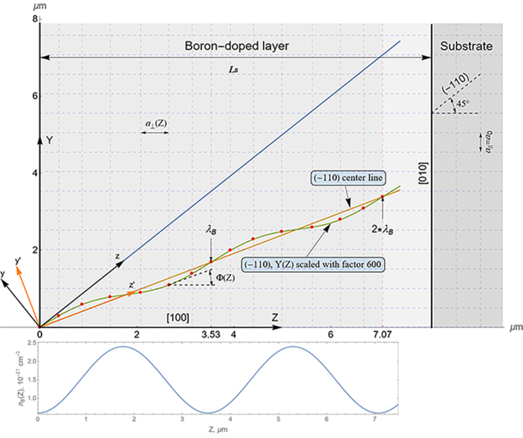
As a case study we consider a heterocrystal consisting of two parts: (1) the oriented single diamond (100) substrate and (2) the diamond crystal doped with boron atoms whose concentration varies along the crystallographic axis (the direction), see Fig. 1. This causes the lattice constant to vary along . In the direction (the crystallographic axis) the in-plane lattice constant , i.e. the one measured along the and crystallographic directions, does not change, being equal to its equilibrium value Å in the diamond crystal. Following Refs. [34, 53, 54, 55] one considers the linear dependence of on the boron concentration:
| (1) |
The values of the coefficient , calculated using the Vegard’s law [56] and in the linear approximation for average atomic volume [54] are as follows:
| (4) |
For brevity, the values calculated according to Refs. [54] and [56] are notated below as and , respectively. Other quantities that depend on are similarly notated.
In boron-doped diamonds grown by the MPCVD method the concentration of the boron atoms does not exceed a few percent of the concentration cm-3 of carbon atoms in the diamond crystal [34, 57]. Therefore, a strong inequality
| (5) |
is implied below.
The change in leads to a distortion of the crystallographic directions that are not parallel to the plane. In particular, the angle between the plane (shown by the blue line in the figure) and the axis deviates from its value of in the single crystal (the dashed line). In the doped crystal the angle changes with so that
| (6) |
Hence, the profile of the deformed plane is calculated as follows:
| (7) | |||||
| with | (8) |
Because of the condition (5), the strong inequality is valid for all values of . However, it is important to know the explicit dependence in order to choose (i) the direction of the incident beam that provides the optimal conditions for channeling, and (ii) the orientation of the cone within which the intensity of the emitted radiation is maximised.
For further reference let us write the profile (7) in terms of the coordinates where the axis is aligned with the [-110] axial direction and the axis lies within the (-110) plane in the substrate, see Fig. 1. Using the approximation one obtains
| (9) |
Note that thickness of the doped layer along the direction is calculated as where is the thickness along the axis, see Fig. 1.
Eqs. (8) and (9) allow the bending profile to be derived for any dependence of the dopant concentration. The data on can be collected in the process of the doped-diamond growing.
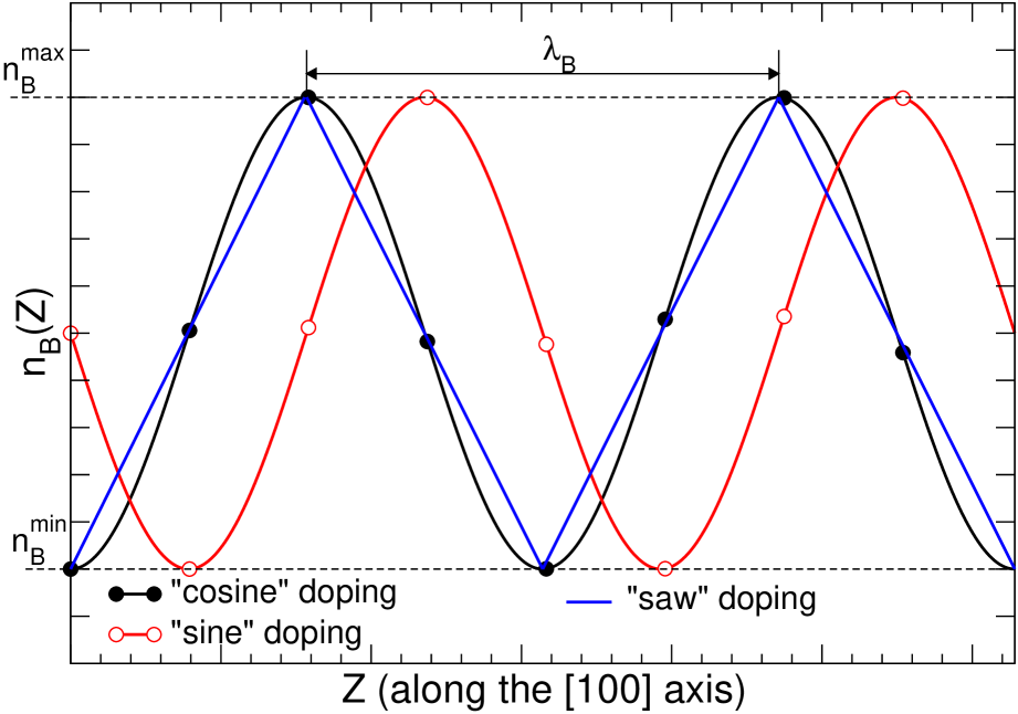
Firstly, derive explicit expressions for the profiles corresponding to several ideally periodic boron doping dependencies , in which the dopant concentration varies from to with fixed period measured along the axis:
| (10a) | |||||
| (10b) | |||||
| (10e) | |||||
Here and in the last equation .
These dependencies are shown in Fig. 2.
Using the aforementioned dependencies in Eqs. (7)-(8) one writes the profile (9) as follows:
| (11) |
where is a periodic function. Its explicit expression reads111To avoid confusion with the names of the trigonometric functions used in this expression and the terms ”cosine” and ”sine” we note that the latter denote the doping dependencies, Eqs. (10a)-(10b).:
| (17) |
The term on the right-hand side of Eq. (11) represents the undulatory part of the profile. Its period is and the amplitude value is for the ”sine” and ”cosine” doping and to a smaller value of for the ”saw” doping (see also Fig. 12 in Appendix A which compares the profiles of ). For boron-doped diamonds produced by Microwave Plasma Chemical Vapor Deposition (MPCVD), typical values of are in the range microns and cm-3 [58]. These values together with from Eq. (4) lead to an estimate of Å.
The term proportional to on the right-hand side of Eq. (11) determines the direction of the centreline of the undulating profile (i.e., the undulator axis, labelled as in Fig. 1) with respect to the (-110) plane in the substrate. Its derivative gives the angle between the plane and the centreline:
| (18) |
The value of can be in the range of several hundred microradians for boron-doped diamonds.
As mentioned in Section I, the PB boron-doped segment of the hetero-crystal cannot be separated from the substrate. As a rule, the thickness of the substrate in the direction (hundred of microns and more) is notably larger than the thickness of the doped layer (few tens of microns). Therefore, in the experiment, in order to increase the intensity of the undulator radiation, the beam of particles must be incident on the PB segment to avoid the decrease in the number of channeling particles due to the dechanneling in the substrate [44]. In this case, to increase the acceptance of the beam particles into the channeling mode, the angle between the beam direction and a tangent to the PB profile at the crystal entrance must be much smaller than Lindhard’s critical angle [1]. Ideally, the beam must be aligned with the tangent line, the angle of which with respect to the -axis is
| (19) |
Note that for the for the ”cosine” and the ”saw” doping while for the ”sine” doping . The latter case may be preferable for channeling experiments as it requires the beam to be aligned with the centreline, the direction of which can be precisely defined.
The derivative calculated at determines the direction of the tangent line at the end of the boron-doped layer. This quantity determines the mean angle of the channeling particles at the entrance to the substrate. By a proper choice of the dopant concentration in the vicinity of it is possible to fulfill the condition, thereby increasing the number of particles accepted into the channeling regime in the substrate.
The general formulae (6)-(9) allow the bending profile to be evaluated for any dependence of the boron concentration on the coordinate. In particular, the dependence , used in the process of growing boron-doped diamonds and measured by the secondary-ion mass spectrometry (SIMS) method [41], can serve as input data to calculate . To illustrate this, in Section III.2 we model a quasi-periodic doping which resembles the doping profile in the periodically bent sample grown using the MPCVD method [58].
III Numerical results
III.1 Case study I
In this section we present the results of numerical simulations of the channeling process and the radiation emission by MeV electrons and 530 MeV positrons incident on the oriented diamond crystal periodically doped with boron. The parameters of the ”saw”-doped layer used in the simulations correspond to those described in Ref. [41] and are as follows: (i) the doping period in the [100] direction m, (ii) the number of periods , (iii) the minimum and maximum values of the boron concentrations used in the process of producing the layer by MPCVD are cm-3 and cm-3.
In the cited paper the coefficient , which enters into the dependence (1) of the diamond lattice constant on the boron concentration, was calculated according to Ref. [54]. Since the available experimental and theoretical data on (see, e.g., Fig. 2 in [41]) do not allow one a definite choice of its value, the current simulations were performed for both values of given in Eq. (4).
III.1.1 Description of the profile
Figure 3 shows the profiles (solid lines) along the (-110) planar direction calculated for and . For brevity, the notations P and P are used to distinguish the profiles. The dashed lines represent the centrelines; the corresponding values of , Eq. (18), are indicated explicitly. The amplitudes of the undulatory parts of the profiles are Å and Å. The period m is the same for each profile. The vertical line marks the thickness of the doped layer, m. In the point the absolute values of the angle (19) between the tangent lines and the axis are
| (20) |
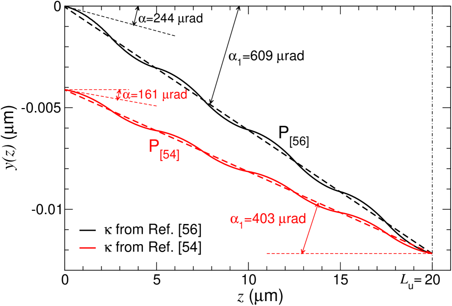
Apart from the quantities mentioned above, it is instructive to calculate the curvature of the profiles. In a bent crystal, this quantity defines the centrifugal force acting on the channeling particle in the co-moving frame. The condition for a stable channeling [59] implies that is less than the maximum interplanar force , which holds the particle in the channel. Using Eqs. (11) and (17), one derives the general expression and, as a consequence, the values cm-1 and cm-1. In the framework of the continuous potential model [1], the maximum interplanar force in the diamond (110) channel is estimated to be GeV/cm. Then, the values of the bending parameter defined as the ratio are as follows:
| (23) |
Note that for both profiles the curvature radius is constant. Therefore, the periodic component of each profile is a series of arcs of circles of equal radius but alternating sign of the curvature.
III.1.2 Results of atomistic simulations of the channeling and photon emission processes
For each profile, electron and positron passage simulations and photon emission spectra calculations were performed for the following two different beam–crystal alignments (A):
-
A1:
The incident beam velocity is aligned with the (-110) planar direction in the substrate (i.e., parallel to the axis in Figs. 1 and 3).
It should be noted that this alignment was used in Ref. [41] (see Sections 5.1 and 5.2 there).
-
A2:
The velocity is aligned with the tangent line to the profile at .
The root-mean square divergences of the electron and positron Gaussian beams used in the simulations were calculated using the full width at half maximum data from Refs. [60, 61]: and (270,27) rad for the electron and positron beams, respectively. To ensure statistical reliability of the results, in each simulation (i.e., for each projectile type, each profile and alignment) approximately trajectories were simulated.
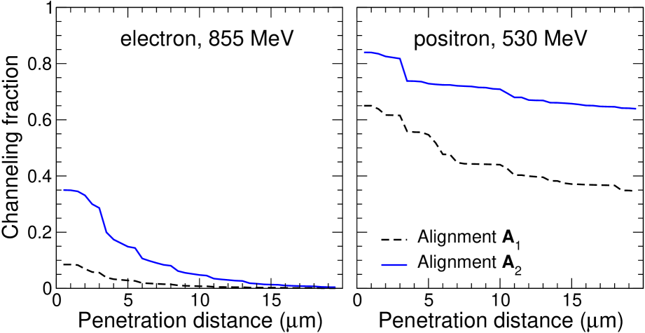
The impact of the choice of the beam–crystal orientation on the channeling efficiency is illustrated in Fig. 4, which compares the dependence of the fraction of particles, which were accepted in the channeling mode at the entrance, on the penetration distance. The left and right panels refer to the electrons and positrons, respectively. In both panels, the dashed curves show the dependence obtained for the alignment A1, the solid curves – for A2. All dependencies shown refer to the profile P.
In the case of A2, the fractions of the particles accepted at the entrance are about 0.4 and 0.8 for the electrons and positrons, respectively. These values correlate with the previously calculated data for a straight diamond (110) channel: for 855 MeV electrons [62, 49] and for 530 MeV positrons [49]. To see the correspondence, recall that for an ideally collimated beam the acceptances in the bent and straight channels are related as (see, e.g., [3]) and use the values given in (23). The remaining discrepancy could be attributed to the fact that the simulations [62] were performed for the beams with non-zero divergence.
Comparing the dashed and the solid curves in Fig. 4, it can be seen that the fractions are much smaller for the A1 orientation. The decrease is much more pronounced for electrons. This can be understood comparing the angle rad with Lindhard’s critical angle in the bent diamond (110) channel. In the straight channel, where eV is the depth of the interplanar potential. In the bent channel, this value is multiplied by a factor (see, e.g., [63]). Using the values , one finds and rad for the electrons and positrons, respectively. This estimate shows that for the electrons and, therefore, a small fraction of the beam incident along the axis is accepted. In contrast, the inequality obtained for positrons significantly increases the probability of being captured in the channeling regime.
A similar analysis performed for the profile P shows that the fractions for the A2 orientation are slightly reduced due to the larger values of (see Eq. (23)). In contrast, the fraction of channeling particles for the A1 orientation virtually disappears for both types of projectiles. The estimates show that in this case the angle exceeds leading to a strong reduction in the number of accepted particles.
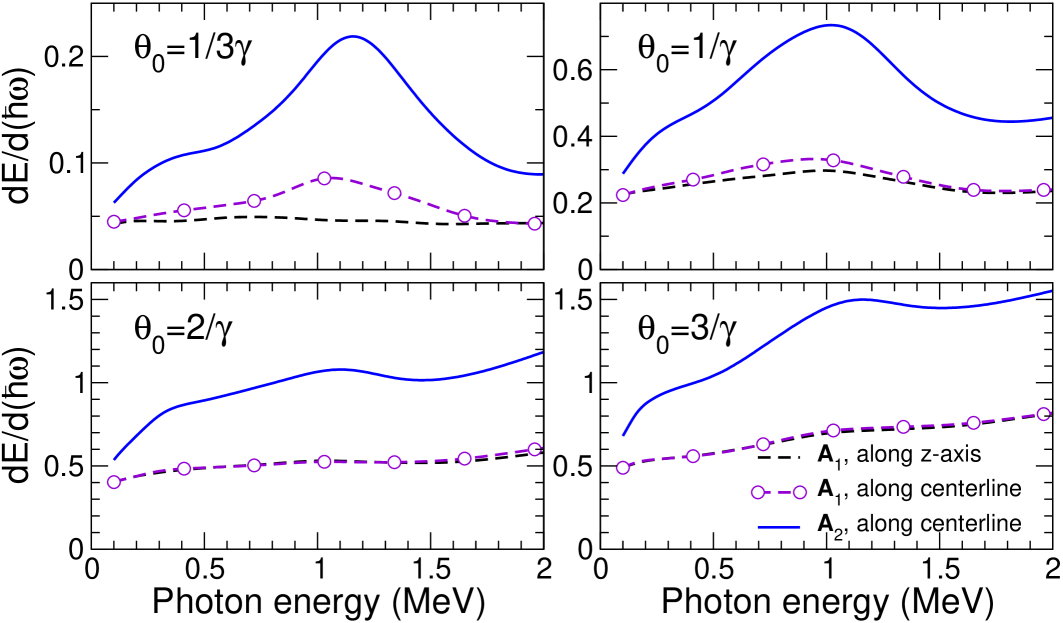
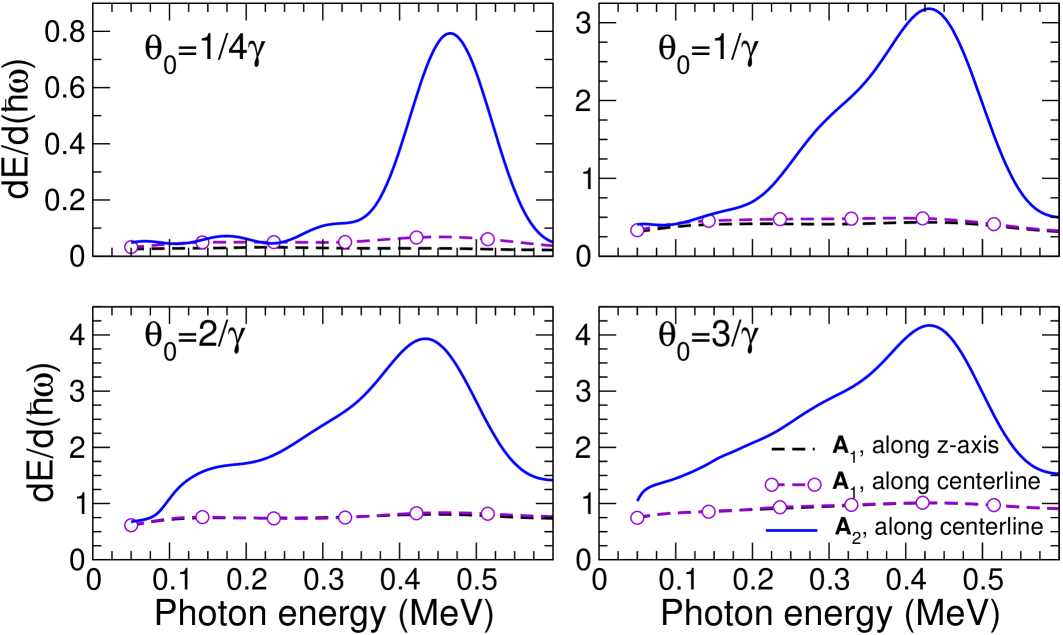
The differences in channeling efficiency for the two orientations and for the two profiles are clearly visible in the spectral distributions of the emitted radiation, shown in Figs. (5)-(6) for the profile P and in Figs. (7)-(8) for P.
A particle channeled in a periodically bent crystal, experiences two types of quasi-periodic motion: the channeling oscillations and the crystal undulator (CU) oscillations due to the periodicity of the bent profile. These motions are very similar to the undulatory motion. As a result, for each value of the emission angle the constructive interference of the waves occurs at some particular equally spaced frequencies (harmonics), so that the spectral distribution consists of a series of narrow peaks. As a rule, the characteristic frequency of the channeling oscillations exceeds greatly that of the CU ones and, therefore, the peak(s) of the channeling radiation [17] are located at much higher photon energies than the peaks of CU radiation (CUR) [4].
The spectral distributions of radiation shown in Figs. (5)-(8) refer to the photon energy range where CUR dominates.
For each simulated trajectory, the spectral-angular distribution of radiation emitted within the solid angle (where and are the polar angles of the emission direction) is calculated numerically following the algorithm outlined in Refs. [45, 4]. The spectral distribution of energy radiated within the cone along any chosen direction and averaged over all trajectories is calculated as follows:
| (24) |
where summation is made over all simulated trajectories of the total number .
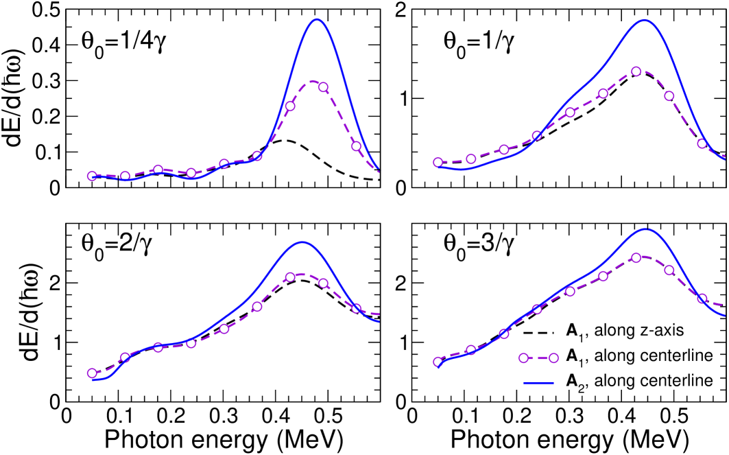
The structure of each of the figures is the same and it is as follows. The four graphs correspond to different emission cones (as indicated) measured in units of equal to approximately 0.96 and 0.60 mrad for the 530 and 855 MeV projectiles, respectively. The cones for MeV and for 855 MeV shown in the upper left graphs are close to the value of mrad used in Ref. [41]. The dashed curves refer to the spectra calculated for the A1 beam-crystal alignment: (i) the ones without symbols stand for the emission cone is chosen along the incident beam velocity, (ii) the curves with open circles show the intensity of the radiation, which is emitted in the cone along the profile centreline. The solid curves refer to the radiation emission along the centreline calculated for the A2 alignment.
The common feature of both types of the projectile, both profiles and all emission cones, is that the most intense radiation is emitted when the beam impinges the crystal along the tangent to the profile. This is not surprising since the A2 orientation maximises the number of channeling particles emitting CUR, whose powerful first harmonic maxima are seen in the photon energy range 0.4-0.5 MeV for the positrons and 0.5-1.5 MeV for the electrons.
The energy of the fundamental harmonic of the undulator radiation can be calculated as follows (see, e.g., [64, 5]):
| (25) |
The undulator parameter is related to the mean square velocity of the particle in the transverse direction: . In a CU this parameter accounts for both the undulator oscillations and the channeling oscillations [65]:
| (26) |
It can be shown that for an ultra-relativistic particle moving along the periodically bent channel (11) with for the ”cosine” and ”sine” doping, and for the ”saw” doping. For positron channeling, assuming the channeling oscillations are harmonic, one relates the value of averaged over the amplitude of channeling oscillations to the depth of the interplanar potential: (see, e.g., [4], Eq. (B.5)).
For the smallest values of the emission cones and , the positions of the peaks are in a very good agreement with the values calculated from Eq. (25). Increase in results in the enhancement of the radiation in the off-axis directions, which is emitted at lower photon energies energies. As a result, the peak become broader and its position is red-shifted.
It can be seen that for the A1 beam-crystal alignment the calculated spectra are very sensitive to the value of the coefficient , Eqs. (1)-(4), chosen to model the bending profile. As mentioned above, for the fraction of the particles accepted in the channeling mode is negligibly small. Therefore, in this case almost all beam particles experience the over-barrier motion and instead of CUR they emit the incoherent bremsstrahlung radiation, which produces a smooth background in the spectral distribution. This is clearly seen in Figs. (7)-(8) for both electrons and positrons and for all emission cones.
For the smaller value of the coefficient, , the spectral distributions of the radiation emitted in the cones along the centreline (dashed lines with symbols) are, basically, similar in shape to those obtained for the A2 alignment but less intense due to the smaller number of the particles that channel in the periodically bent channel. The distributions shown in the dashed curves without symbols represent the radiation from the channeling particles but emitted off-axis, i.e. not along the centreline, which is the undulator axis, but in the cone whose axis is inclined at the angle rad to the centreline. From the general theory of the undulator radiation (see, e.g., [66]) it is known that the off-axis radiation is less intense than the on-axis radiation and that its characteristic energy is red-shifted. The latter property follows directly from Eq. (25) where the emission angle must be considered to be centered at . Therefore, the term in the denominator reduces the energy . The shift in the peak position can be clearly seen for in the spectral distribution of radiation emitted by positrons in the small emission cone , Fig. 5. In the electron spectrum, top left graph in Fig. 6, it is much less pronounced, but still distinguishable as a hump around MeV. For larger emission cones, at , the difference between the on-axis and off-axis spectral distributions virtually disappears because these cones collect all the emitted radiation.

III.2 Case study II
In this section we present the results of numerical simulations of the channeling process and the radiation emission by MeV electrons and 530 MeV positrons in a diamond crystal doped quasi-periodically.
We consider a quasi-periodic doping, which models the doping profile in the sample grown using the MPCVD method [58].
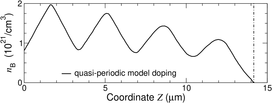
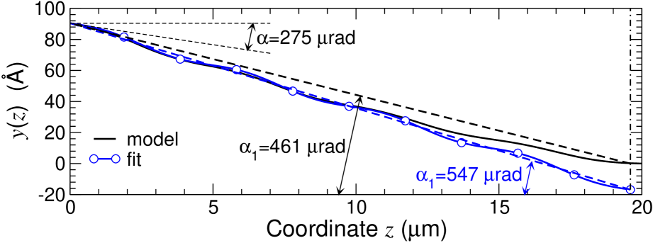
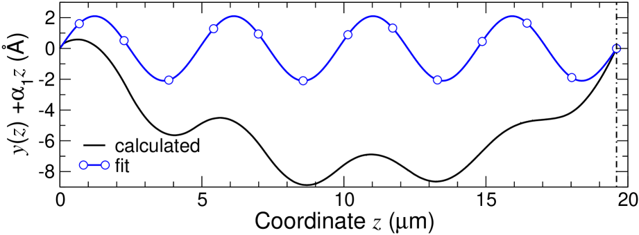
The boron concentration versus distance from the substrate along the [100] direction is shown in Fig. 9, top graph. The doped layer of approximately 14 m thickness has four periods, which vary in the the range 3-4 m. Except for the final segment of about 2 m, the amplitude of increases nearly linearly with . It can be seen that there are large deviations from the dependence in the case of ideal ”saw” doping, see Fig. (2).
The corresponding model profile of the (-110) plane, calculated using Eqs. (6)-(9) with , is shown in the middle graph by the solid black line. The (black) dashed line connects the first, , and last, m, points of the profile. The solid blue curve with open circles shows the fit, , with rad (shown in the graph), Å, and m. The (blue) dashed line shows the centerline of the fit. At the entrance point the tangent lines to the fitting curve and to the calculated profile are inclined by the same angle of 275 rad to the axis, which is aligned with the (-110) planar direction in the substrate.
The quasi-periodic (for the model profile) and periodic (for the fit) parts of the profiles are shown in the bottom graph. They are calculated by subtracting the linear dependencies from .
For the calculated profile and for its fit, electron and positron passage simulations and photon emission spectra calculations were performed. The parameters of the beams used in the simulations were as described Section III.1.2. The spectra were calculated for the beam–crystal alignment A2, i.e. directing the beam velocity with the tangent line to the profile at .
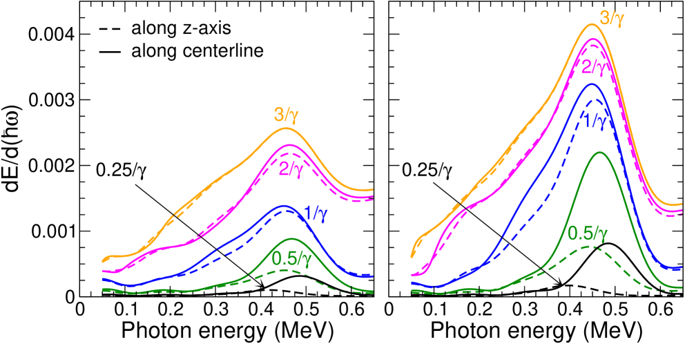
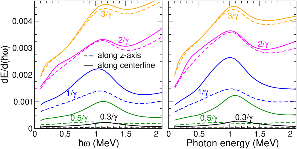
Spectral distributions are shown in Figs. 10 (for 530 MeV positrons) and 11 (for 855 MeV electrons). The structure of each of the figures is the same and it is as follows. The left and right graphs represent the spectra calculated for the model profile and for its fit, correspondingly. The solid curves show the emission in the cone aligned with the centerline of the profile. The dashed curves correspond to the emission along the -axis. The emission cones (as indicated) are measured in units of equal to approximately 0.96 and 0.60 mrad for the 530 and 855 MeV projectiles, respectively.
The feature common to both positron and electron spectra is that for the small emission cone (see Fig. 9, middle graph) the emission in the forward direction (i.e. along the centerline) is significantly more intense. This is in line with the arguments presented in Section III.1.2. As discussed in the main text, the intensity of radiation emitted in small cones is very sensitive to the direction of the cone relative to the centerline of the profile. For larger cones both geometries of the photon emission produce virtually the same result.
IV Conclusion and outlook
In this study, we have conducted a theoretical analysis of the profiles of the planar (-110) crystallographic direction in the diamond layer doped with boron atoms. The general formalism outlined has been applied to derive the profiles for periodic doping following the ideal dependencies (”cosine”, ”sine” and ”saw”) of the boron concentration on the distance in the crystalline medium as well as those measured by the SIMS method in the samples, grown at ESRF by MPCVD method, to be used in channeling experiments at the MAMI facility. A detailed analysis of the geometry of the calculated profiles has been carried out.
Numerical simulations of the channeling and photon emission processes have been carried out for 855 MeV electron and 530 MeV positron beams incident on boron-doped diamond with a four-period bending profile (the bending period is m) corresponding to the ”saw” doping. It is shown that the channeling efficiency and the intensity of the crystalline undulator radiation strongly depend on the orientation of the incident beam relative to the bent channel profile at the entrance to the boron-doped layer. The orientation that maximizes both mentioned quantities implies the angle between the beam direction and the tangent line to the channel’s profile to be smaller than Lindhard’s critical angle. The direction of the tangent can be calculated unambiguously from the dependence of the dopant concentration, , on the coordinate along the [100] axis. In a particular case of the ”sine” doping the tangent line is along the centreline of the periodically bent channel. This doping scheme could be advantageous for the use in channeling experiments, since it does not require additional alignment with the incident beam.
In the context of a diamond hetero-crystal, it is not possible to separate the boron-doped segment from the single diamond substrate. Consequently, the particles propagate in the substrate after passing through the periodically bent part. In Ref. [44] it was demonstrated that in the case of positrons a comparatively large fraction of the projectile move through the substrate in the channeling regime and emit channeling radiation. For electrons this fraction is negligibly small for the electrons. The remaining beam particles undergo the overbarrier motion, thereby emitting incoherent bremsstrahlung. Within the photon energy range of MeV, both radiation mechanisms yield a smooth and largely constant background in the spectral distribution. Consequently, they do not impact the profile of the CUR, which is of paramount interest. In the current simulations, this background has not been accounted for.
The results of the spectra calculations have demonstrated that the intensity and the profile of CUR is sensitive to the value of the coefficient , which determines the dependence of the lattice constant on the boron concentration, Eq. (1). The data available in the literature do not permit a definitive choice of its value. In order to address this issue, the atomistic-level molecular dynamics simulations are currently being conducted on boron-doped diamond crystal. The objective of this research is to elucidate the effects of dopant concentration on the lattice constant. Previously, such simulations were performed in Ref. [67] for silicon-germanium superlattices.
Appendix A Periodic part of the profiles due to the ”cosine” and ”saw” doping
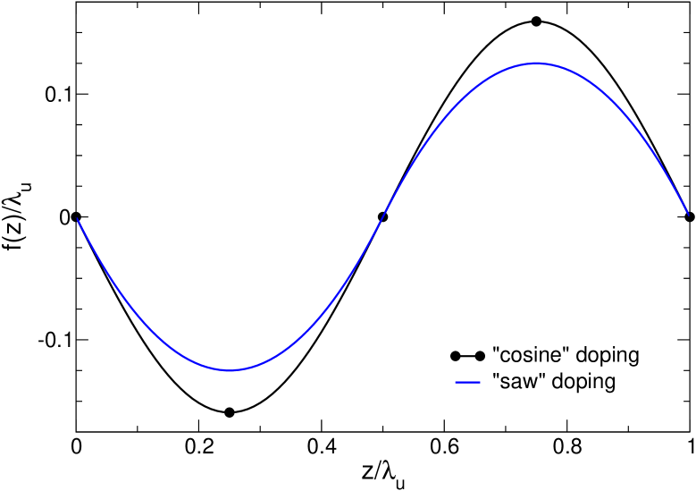
Figure 12 compares the functions , see Eq. (17), calculated for the ”cosine” (solid line with filled circles) and ”saw” (solid line) doping schemes. In the figure, both the abscissa and the ordinate are scaled by the undulator period . In these units, the amplitude values are and for the ”cosine” and ”saw” doping, respectively.
Acknowledgements
We acknowledge support by the European Commission through the N-LIGHT Project within the H2020-MSCA-RISE-2019 call (GA 872196) and the EIC Pathfinder Project TECHNO-CLS (Project No. 101046458). We also acknowledge the Frankfurt Center for Scientific Computing (CSC) for providing computer facilities We are grateful to Hartmut Backe, Werner Lauth, and Thu Nhi Tran Caliste for constructive discussions.
Competing Interests. The authors do not declare any conflicts of interest, and there is no financial interest to report.
Author Contribution.
AVK:
Conceptualization;
Rel-MD simulations;
Analysis of the boron-doped diamond geometry and the results of
atomistic simulations.
Writing – review & editing.
AVS: Project administration;
Conceptualization;
Analysis of the boron-doped diamond geometry and the results of
atomistic simulations.
Writing – review & editing.
All authors reviewed the final manuscript.
References
References
- [1] J. Lindhard, Influence of crystal lattice on motion of energetic charged particles, K. Dan. Vidensk. Selsk. Mat. Fys. Medd. 34, 1 (1965). (https://gymarkiv.sdu.dk/MFM/kdvs/mfm%2030-39/mfm-34-14.pdf).
- [2] U. I. Uggerhøj, The interaction of relativistic particles with strong crystalline fields, Rev. Mod. Phys., 77, 1131-1171 (2005)
- [3] V.M. Biryukov, Yu.A. Chesnokov and V.I. Kotov. Crystal Channeling and its Application at High-Energy Accelerators. (Springer Science & Business Media, 2013).
- [4] A. V. Korol, A. V. Solov’yov, and Walter Greiner, Channeling and Radiation in Periodically Bent Crystals (2nd ed.), (Springer Series on Atomic, Optical, and Plasma Physics, vol. 69. Springer-Verlag, Heidelberg, New York, Dordrecht, London, 2014).
- [5] A.V. Korol and A.V. Solov’yov, Novel Light Sources beyond Free Electron Lasers (Springer Nature Switzerland AG, 2022).
- [6] A. Mazzolari, M. Romagnoni, R. Camattari, E. Bagli, L. Bandiera, G. Germogli, V. Guidi, and G. Cavoto, Bent crystals for efficient beam steering of multi TeV-particle beams, Eur. Phys. J. C 78, 720 (2018). (https://doi.org/10.1140/epjc/s10052-018-6196-z).
- [7] A.G. Afonin, V.T. Baranov, V.M. Biryukov, M.B.H. Breese, V.N. Chepegin, Yu.A. Chesnokov, V. Guidi, Yu.M. Ivanov, V.I. Kotov, G. Martinelli, W. Scandale6, M. Stefancich, V.I. Terekhov, D. Trbojevic, E.F. Troyanov, and D. Vincenzi, High-Efficiency Beam Extraction and Collimation Using Channeling in Very Short Bent Crystals, Phys. Rev. Lett. 87, 094802 (2001). (https://doi.org/10.1103/PhysRevLett.87.094802).
- [8] W. Scandale, G. Arduini, F. Cerutti, M. Garattini, S. Gilardoni, A. Masi, D. Mirarchi, S. Montesano, S. Petrucci, S. Redaelli, R. Rossi, D. Breton, L. Burmistrov, S. Dubos, J. Maalmi, A. Natochii, V. Puill, A. Stocchi, D. Sukhonos, E. Bagli, L. Bandiera, V. Guidi, A. Mazzolari, M. Romagnoni, F. Murtas, F. Addesa, G. Cavoto, F. Iacoangeli, F. Galluccio, A.G. Afonin, M.K. Bulgakov, Yu.A. Chesnokov, A.A. Durum, V.A. Maisheev, Yu.E. Sandomirskiy, A.A. Yanovich, A.A. Kolomiets, A.D. Kovalenko, A.M. Taratin, G.I. Smirnov, A.S. Denisov, Yu.A. Gavrikov, Yu.M. Ivanov, L.P. Lapina, L.G. Malyarenko, V.V. Skorobogatov, G. Auzinger, T. James, Comprehensive study of beam focusing by crystal devices, Phys. Rev. Accel. Beams 21, 014702 (2018) (https://doi.org/10.1103/PhysRevAccelBeams.21.014702).
- [9] A. Sytov, G. Kube, L. Bandiera, P. Cirrone, H. Ehrlichmann, V. Guidi, V. Haurylavets, M. Romagnoni, M. Soldani, M. Stanitzki, M. Tamisari, V. Tikhomirov, K. Wittenburg, and A. Mazzolari, First design of a crystal-based extraction of 6 GeV electrons for the DESY II Booster Synchrotron, Eur. Phys. J. C 82, 197 (2022) (https://doi.org/10.1140/epjc/s10052-022-10115-4).
- [10] G.B. Sushko, A.V. Korol, and A.V. Solov’yov, Extremely brilliant crystal-based light sources, Europ. Phys. J. D 76, 166 (2022).
- [11] A.V. Korol and A.V. Solov’yov, Atomistic modeling and characterizaion of light sources based on small-amplitude short-period periodically bent crystals, Nucl. Inctrum. Meth. B 537, 1 (2023).
- [12] http://www.mbnresearch.com/TECHNO-CLS/Main
- [13] G.B. Sushko, A.V. Korol, and A.V. Solov’yov, Intense -ray light sources based on oriented single crystals, Phys. Rec. Accel. Beams 27, 100703 (2024) (https://doi.org/10.1103/PhysRevAccelBeams.27.100703).
- [14] A.V. Korol, A.V. Solov’yov, and Walter Greiner, Coherent radiation of an ultrarelativistic charged particle channeled in a periodically bent crystal, J. Phys. G: Nucl. Part. Phys. 24, L45-L53 (1998) (https://doi.org/10.1088/0954-3899/24/5/001).
- [15] A.V. Korol, A.V. Solov’yov, and Walter Greiner, Channeling of Positrons through Periodically Bent Crystals: On the Feasibility of Crystalline Undulator and Gamma-Laser, Int. J. Mod. Phys. E 13, 867-916 (2004) (https://doi.org/10.1142/S0218301304002557).
- [16] M. Tabrizi, M., A. V. Korol, A. V. Solov’yov, and W. Greiner, Feasibility of an electron-based crystalline undulator. Phys. Rev. Lett. 98, 164801 (2007) (https://doi.org/10.1103/PhysRevLett.98.164801).
- [17] M. A. Kumakhov, On the theory of electromagnetic radiation of charged particles in a crystal. Phys. Lett. 57A, 17 (1976) (https://doi.org/10.1016/0375-9601(76)90438-2).
- [18] S. Bellucci, S. Bini, V.M. Biryukov, Yu.A. Chesnokov, S. Dabagov, G. Giannini, V. Guidi, Yu.M. Ivanov, V.I. Kotov, V.A. Maisheev, C. Malagù, G. Martinelli, A. A. Petrunin, V.V. Skorobogatov, M. Stefancich, and D. Vincenzi, Experimental Study for the Feasibility of a Crystalline Undulator, Phys. Rev. Lett. 90, 034801 (2003) (https://doi.org/10.1103/PhysRevLett.90.034801).
- [19] P. Balling, J. Esberg, K. Kirsebom, D.Q.S. Le, U.I. Uggerhøj, S.H. Connell, J. Härtwig, F. Masiello. and A. Rommeveaux, Bending diamonds by femtosecond laser ablation, Nucl. Instrum. Meth. B 267, 2952-2957 (2009) (http://dx.doi.org/10.1016/j.nimb.2009.06.109).
- [20] V. Guidi, A. Antonioni, S. Baricordi, F. Logallo, C. Malagù, E. Milan, A. Ronzoni, M. Stefancich, G. Martinelli, and A. Vomiero, Tailoring of silicon crystals for relativistic-particle channeling, Nucl. Instrum. Meth. B 234, 40 (2005) (https://doi.org/10.1016/j.nimb.2005.01.008).
- [21] E. Bagli, L. Bandiera, V. Bellucci, A. Berra, R. Camattari, D. De Salvador, G. Germogli, V. Guidi, L. Lanzoni, D. Lietti, A. Mazzolari, M. Prest, V. V. Tikhomirov and E. Valla. Experimental evidence of planar channeling in a periodically bent crystal. Eur. Phys. J. C 74, 3114 (2014) (https://doi.org/10.1140/epjc/s10052-014-3114-x).
- [22] V. Guidi, A. Mazzolari, G. Martinelli, and A. Tralli, Design of a crystalline undulator based on patterning by tensile Si3N4 strips on a Si crystal, Appl. Phys. Lett. 90, 114107 (2007), (https://doi.org/10.1063/1.2712510).
- [23] V. Guidi, L. Lanzoni, and A. Mazzolari. Patterning and modeling of mechanically bent silicon plates deformed through coactive stresses, Thin Solid Films 520, 1074 (2011), (https://doi.org/10.1016/j.tsf.2011.09.008).
- [24] L. Malagutti, L. Bandiera, F. Bonafè, N. Canale, D. De Salvador, P. Fedeli, V. Guidi, A.V. Korol, F. Mancarella, R. Negrello, G. Paternò, M. Romagnoni, F. Sgarbossa, A.V. Solov’yov, A. Sytov, D. Valzani, A. Mazzolari From simulation to fabrication: Realizing silicon crystalline undulators with silicon nitride stressor layer patterning, Nucl. Instrum. Meth. A 1076, 170480 (2025) (https://doi.org/10.1016/j.nima.2025.170480).
- [25] R. Camattari, G. Paternò, M. Romagnoni, V. Bellucci, A. Mazzolari, and V. Guidi, Homogeneous self-standing curved monocrystals, obtained using sandblasting, to be used as manipulators of hard X-rays and charged particle beams. J. Appl. Cryst. 50, 145-151 (2017) (https://doi.org/10.1107/S1600576716018768).
- [26] V. Bellucci, R. Camattari, V. Guidi, A. Mazzolari, G. Paterno, G. Mattei, C. Scian and L. Lanzoni, Ion implantation for manufacturing bent and periodically bent crystals. Appl. Phys. Lett. 107, 064102 (2015), (https://doi.org/10.1063/1.4928553).
- [27] A.V. Korol, A.V. Korol, Solov’yov, and W. Greiner, Photon emission by an ultra-relativistic particle channeling in a periodically bent crystal. Int. J. Mod. Phys. E 8, 49 (1999) (https://doi.org/10.1142/S0218301399000069).
- [28] V.G. Baryshevsky, I.Ya. Dubovskaya, A.O. Grubich, Generation of -quanta by channeled particles in the presence of a variable external field, Phys. Lett. A 77, 61-64 (1980) doi = 10.1016/0375-9601(80)90637-4,
- [29] K. Kaleris, E. Kaselouris, V. Dimitriou, E. Kaniolakis-Kaloudis, M. Bakarezos, M. Tatarakis, N. A. Papadogiannis, G.B. Sushko, A.V. Korol, A.V. Solov’yov Narrowband -ray radiation generation by acoustically driven crystalline undulators Phys. Rev. Accel. Beams 28, 033502 (2025) (https://doi.org/10.1103/PhysRevAccelBeams.28.033502).
- [30] M.B.H. Breese, Beam bending using graded composition strained layers, Nucl. Instrum. Meth. B 132, 540 (1997) (https://doi.org/10.1016/S0168-583X(97)00455-2).
- [31] U. Mikkelsen and E. Uggerhøj, A crystalline undulator based on graded composition strained layers in a superlattice, Nucl. Instrum. Meth. B 160, 435-439 (2000) (https://doi.org/10.1016/S0168-583X(99)00637-0).
- [32] R.O. Avakian, K.N. Avetyan, K.A. Ispirian, E.G. Melikyan, Bent crystallographic planes in gradient crystals and crystalline undulators, Nucl. Instrum. Meth. A 508, 496-499 (2003) (https://doi.org/10.1016/S0168-9002(03)01656-5).
- [33] A. Sakai, Silicon-germanium (SiGe) crystal growth using molecular beam epitaxy, In: Silicon-Germanium (SiGe) Nanostructures. Woodhead Publishing Series in Electronic and Optical Materials, Shiraki, Y., Usami, N. (eds.) (Woodhead Publishing, Cham, 2011), pp.83–116 (https://doi.org/10.1533/9780857091420.2.83).
- [34] S.H. Connell, J. Härtwig, A. Masvaure, D. Mavunda, T.N. Tran Thi, Towards a crystal undulator. In: Engelbrecht, C., Karataglidis, S. (eds.), Proceedings of the 59th Annual Conference of the South African Institute of Physics (SAIP2014), pp. 169–174. (University of Johannesburg, Johannesburg, 2015) (https://events.saip.org.za/event/34/attachments/1143/1398/SAIP2014-169.pdf).
- [35] H. Backe, D. Krambrich, W. Lauth, K. K. Andersen, J. L. Hansen, and U.K. Uggerhøj, Radiation emission at channeling of electrons in a strained layer Si1-xGex undulator crystal, Nucl. Instrum. Meth. B 309, 37-44 (2013) (https://doi.org/10.1016/j.nimb.2013.03.047).
- [36] H. Backe, D. Krambrich, W. Lauth, K. K. Andersen, J. L. Hansen, and U. I. Uggerhøj, Channeling and radiation of electrons in silicon single crystals and Si1-xGex crystalline undulators, J. Phys. Conf. Ser. 438, 012017 (2013) (https://doi.org/10.1088/1742-6596/438/1/012017).
- [37] H. Backe, D. Krambrich, W. Lauth, J. Lundsgaard Hansen, U.K.I. Uggerhøj, X-ray emission from a crystal undulator: Experimental results at channeling of electrons, Nuovo Cimento C 34, 157-165 (2011) (https://doi.org/10.1393/ncc/i2011-10938-2).
- [38] T. N. Wistisen, K. K. Andersen, S. Yilmaz, R. Mikkelsen, J. L. Hansen, U. I. Uggerhøj, W. Lauth, and H. Backe, Experimental realization of a new type of crystalline undulator, Phys. Rev. Lett. 112, 254801 (2014) (https://doi.org/10.1103/PhysRevLett.112.254801).
- [39] U. I. Uggerhøj and T. N. Wistisen, Intense and energetic radiation from crystalline undulators, Nucl. Instrum Meth. B 355, 35-39, (2015) (https://doi.org/10.1016/j.nimb.2015.02.069).
- [40] U. I. Uggerhøj, T. N. Wistisen, J. L. Hansen, W. Lauth, and P. Klag, Radiation collimation in a thick crystalline undulator, Eur. Phys. J. D 71, 124 (2017) (https://doi.org/10.1140/epjd/e2017-70720-y).
- [41] H. Backe, W. Lauth, P. Klag, and Thu Nhi Tran Caliste, Planar channeling of 855 MeV electrons in a boron-doped (110) diamond undulator - a case study, Nucl. Instrum. Meth. A 1073, 170236 (2025) (https://doi.org/10.1016/j.nima.2025.170236).
- [42] Hartmut Backe, José Baruchel, Simon Bénichou, Rébecca Dowek, David Eon, Pierre Everaere, Lutz Kirste, Pascal Klag, Werner Lauth, Patrik Straňák, and Thu Nhi Tran Caliste, Observation of narrow-band radiation from a boron-doped diamond superlattice with an 855 MeV electron beam - with prospects arXiv:2504.17988 (2025) (https://doi.org/10.48550/arXiv.2504.17988).
- [43] A.V. Pavlov, A.V. Korol, V.K. Ivanov, and A.V. Solov’yov, Channeling of electrons and positrons in straight and periodically bent diamond(110) crystals, Europ. Phys. J. D 74, 21 (2020) (https://doi.org/10.1140/epjd/e2019-100224-3).
- [44] A.V. Pavlov, A.V. Korol, V.K. Ivanov, and A.V. Solov’yov, Channeling and radiation of electrons and positrons in the diamond heterocrystals, St. Petersburg Polytechnic Uni. J.: Phys. Math. 14, 190-201 (2021) (https://doi.org/10.18721/JPM.14414).
- [45] G. B. Sushko, V. G. Bezchastnov, I. A. Solov’yov, A. V. Korol, W. Greiner, A. V. Solov’yov, Simulation of ultra-relativistic electrons and positrons channeling in crystals with MBN Explorer. J. Comp. Phys. 252, 404 (2013) (https://doi.org/10.1016/j.jcp.2013.06.028).
- [46] G. B. Sushko, I. A. Solov’yov, A. V. Solov’yov, Modeling MesoBioNano systems with MBN Studio made easy. J. Mol. Graph. Model. 88, 247 (2019). (https://doi.org/10.1140/epjd/e2015-60424-9).
- [47] I. A. Solov’yov, A. V. Yakubovich, P. V. Nikolaev, I. Volkovets, A. V. Solov’yov, MesoBioNano Explorer – A universal program for multiscale computer simulations of complex molecular structure and dynamics. J. Comp. Phys. 33, 2412 (2012). (https://doi.org/10.1002/jcc.23086).
- [48] A. V. Korol, G. B. Sushko, A. V. Solov’yov, All-atom relativistic molecular dynamics simulations of channeling and radiation processes in oriented crystals. Europ. Phys. J. D 75, 107 (2021). (https://doi.org/10.1140/epjd/s10053-021-00111-w).
- [49] G. B. Sushko, A. V. Korol, and A. V. Solov’yov, Atomistic modeling of the channeling process with and without account for ionising collisions: A comparative study, arXiv:2405.07633v2 (2025) (https://arxiv.org/pdf/2405.07633v2).
- [50] S.T. Picraux, L.R. Dawson, J.Y. Tsao, B.L. Doyle, and S.R. Lee, Structure of layered crystals studied by high energy ion beams, Nucl. Instrum. Meth. B 33, 891-897 (1988) (https://doi.org/10.1016/0168-583X(88)90705-7).
- [51] D. De Salvador, M. Petrovich, M. Berti, F. Romanato, E. Napolitani, A. Drigo, J. Stangl, S. Zerlauth, M. Mühlberger, F. Schäffler, G. Bauer, and P. C. Kelires, Lattice parameter of Si1-x-yGexCy alloys, Phys. Rev. B 61, 13005-13013 (2000) (https://doi.org/10.1103/PhysRevB.61.13005).
- [52] A.V. Korol, W. Krause, A.V. Solov’yov, and W. Greiner, Photon emission by ultra-relativistic positrons in crystalline undulators: the high-energy regime, Nucl. Instrum. Meth. A 483, 455-460 (2002) (https://doi.org/10.1016/S0168-9002(02)00361-3).
- [53] T. Wojewoda, P. Achatz, L. Ortéga, F. Omnés, C. Marcenat, E. Bourgeois, X. Blase, F. Jomard, E. Bustarret, Doping-induced anisotropic lattice strain in homoepitaxial heavily boron-doped diamond, Diamond Rel. Mat. 17, 1302-1306 (2008) (https://doi.org/10.1016/j.diamond.2008.01.040).
- [54] V.V. Brazhkin, E.A. Ekimov, A.G. Lyapin, S.V. Popova, A.V. Rakhmanina, S.M. Stishov, V.M. Lebedev, Y. Katayama, and K. Kato, Lattice parameters and thermal expansion of superconducting boron-doped diamonds, Phys. Rev. B 74, 140502 (2006) (https://doi.org/10.1103/PhysRevB.74.140502).
- [55] F. Brunet, P. Germi, M. Pernet, A. Deneuville, E. Gheeraert, F. Laugier, M. Burdin, and G. Rolland, The effect of boron doping on the lattice parameter of homoepitaxial diamond films, Diamond Rel. Mat. 7, 869-873 (1998) (https://doi.org/10.1016/S0925-9635(97)00316-6).
- [56] L. Vegard, Die Konstitution der Mischkristalle und die Raumfüllung der Atome, Z. Physik 5, 17-26 (1921) (https://doi.org/10.1007/BF01349680).
- [57] Thu Nhi Tran Thi, J. Morse, D. Caliste, B. Fernandez, D. Eon, J. Härtwig, C. Barbay, C. Mer-Calfati, N. Tranchant, J.C. Arnault, T.A. Lafford, J. Baruchel, Synchrotron Bragg diffraction imaging characterization of synthetic diamond crystals for optical and electronic power device applications, J. Appl. Cryst. 50, 561-569 (2017) (https://doi.org/10.1107/S1600576717003831).
- [58] Thu Nhi Tran Thi, Private communication (2024).
- [59] Tsyganov, E. N. Fermilab Preprints TM-682: Some aspects of the mechanism of a charged particle penetration through a monocrystal. & TM-684: Estimates of Cooling and bending processes for charged particle penetration through a monocrystal. (Fermilab, Batavia, 1976).
- [60] H. Backe, W. Lauth, P. Drexler, P. Heil, P. Klag, B. Ledroit, and F. Stieleret, Design study for a 500 Mev positron beam at the Mainz Microtron MAMI, Europ. Phys. J. D 76, 150 (2022). (https://doi.org/10.1140/epjd/s10053-022-00465-9).
- [61] H. Backe, On planar (110) channeling of 500 MeV positrons and electrons in silicon semiconductor detectors, Nucl. Instrum. Meth. A 1059, 168998 (2024) (https://doi.org10.1016/j.nima.2023.168998).
- [62] A.V. Pavlov, A.V. Korol, V.K. Ivanov, and A.V. Solov’yov, Channeling of electrons and positrons in straight and periodically bent diamond(110) crystals. Eur. Phys. J. D 74, 21 (2020) (https://doi.org/10.1140/epjd/e2019-100224-3).
- [63] A. M. Taratin, Particle Channeling in a Bent Crystal, Phys. Part. Nucl. 29, 437-462 (1998) (https://doi.org/10.1134/1.953085).
- [64] Pascal Elleaume, Insertion devices for the new generation of synchrotron sources: A review, Rev. Sci. Instrum., 63, 321-326 (1991) (https://doi.org/10.1063/1.1142744).
- [65] A. V. Korol, A. V., Solov’yov, W. Greiner, The influence of the dechanneling process on the photon emission by an ultra-relativistic positron channeling in a periodically bent crystal. J. Phys. G: Nucl. Part. Phys. 27, 95 (2001) (https://doi.org/10.1088/0954-3899/27/1/307).
- [66] D. F. Alferov, Yu. A. Bashmakov, P. A. Cherenkov, Radiation from relativistic electrons in a magnetic undulator, Sov. Phys. - Uspekhi 32, 200-227 (1989) (https://doi.org/10.1070/PU1989v032n03ABEH002688).
- [67] Matthew D. Dickers, Gennady B. Sushko, Andrei V. Korol, Nigel J. Mason, Felipe Fantuzzi, and Andrey V. Solov’yov, Dopant concentration effects on Si1-xGex crystals for emerging light-source technologies: a molecular dynamics study, Europ. Phys. J. D 78, 77 (2024) (https://doi.org/10.1140/epjd/s10053-024-00870-2).