First principles investigation of zb-TiSn: A promising narrow bandgap semiconductor
Abstract
We have investigated the structural stability of a binary compound TiSn in the zincblende symmetry. The phonon dispersion studies confirms that, TiSn with a nominal composition of 1:1 can exist in zincblende form. No imaginary frequencies are observed indicating the stable bonding nature of Ti-Sn. From the First principles calculations based on density functional theory, the resulting electronic band structure had revealed that zb-TiSn, is a narrow band gap semiconductor with an energy gap of 0.3 eV with GGA-PBE. The bonding nature is identified as polar covalent, determined from charge density difference plots and Bader charge analysis. Further more, the linear optical properties of zb-TiSn are derived from the Khon-Sham eigenvalues.
keywords:
Narrow band gap , First principles , effective mass , semiconductors , mean square displacement , zincblende , TiSn[1]addressline=Dept of Physics, School of Advanced Sciences, organization=Vellore Institute of Technology, city=Vellore, postcode=632014, state=TN, country=Bharat(India)
![[Uncaptioned image]](/html/2505.18940/assets/x1.png)
TiSn in zincblende form is structurally and dynamically stable.
Phonon dispersion shows no imaginary frequencies.
DFT calculations confirm a narrow band gap of 0.3 eV (GGA-PBE).
zb-TiSn is identified as a narrow-gap semiconductor.
Bonding is polar covalent from charge and Bader analysis.
Optical properties suggests that zb-TiSn is applicable in IR-photonics.
1 Introduction
Narrow bandgap semiconductors with energy gap ranging between 0.2 and 0.3 eV, such as Pb-chalcogenides, In1-xGaxAs, In1-xGaxSb, and Si1-xGex, are particularly effective for thermoelectric power generation through the Seebeck effect, efficient at low temperatures[1]. Bismuth telluride (0.14 eV), when alloyed with Sb2Te3 (0.24 eV), exhibits high thermoelectric efficiency near room temperature due to its combination of high carrier mobility and low thermal conductivity, making it suitable for Peltier cooling and waste heat recovery[2]. PbTe (0.32 eV) and its alloys are among the most advanced thermoelectric materials for intermediate temperatures[3], broadening their practical applications. Additionally, Bi2Te3 and Sb2Te3 have demonstrated high sensitivity in temperature sensors, often surpassing conventional thermocouples in microelectronic applications[4].
Beyond thermoelectrics, narrow bandgap materials ( eV) plays a crucial role in photovoltaics (PV) by efficiently absorbing the low-energy photons and enhances the output current density and enables the waste heat utilization in thermophotovoltaic systems. These compound are further suitable in laser power beaming under mid-infrared (3-5 m) light which supports the remote energy delivery and waste heat recovery[5].
In addition to energy-related applications, narrow band gap semiconductors, like InSb (band gap 0.23 eV), exhibits strong thermal excitation of intrinsic carriers, leading to high carrier concentrations. Unlike wide band gap materials, they face doping challenges and have softer mechanical properties, shaping their infrared optoelectronic behavior[6]. Their ability to generate non-equilibrium electron–hole pairs under radiation alters the electrical transport and enables the high-sensitivity infrared detection. With small effective masses, high electron mobility, long carrier lifetimes, strong optical absorption, and low thermal generation, they ensure fast response in infrared sensing and communication[7]. Additionally, the tunable band gaps further enhance their versatility across the infrared spectrum[8].
Similarly, semiconductors such as HgCdTe, with a tunable band gap ranging from approximately 0.14 eV to 0.35 eV, have become essential in infrared detector technology[9]. HgCdTe is a pseudo-binary alloy semiconductor that crystallizes in a zincblende structure and due to its band gap tunability over the 1-30 range, it has evolved into the most versatile material for infrared detection[10], enabling advanced multispectral and dual-band imaging for space borne remote sensing applications[11]. The small band gaps of these materials also make them ideal for ultrafast photonics. PbS (0.4 eV) and Bi (0.14 eV) are particularly advantageous for mode-locked pulse lasers, as narrower band gaps enable broader light absorption, enhancing mode-locking performance and expanding their applications in optical communication and laser technologies[12]. Hence, there is considerable interest in designing and developing narrow band gap semiconductors for various applications.
The experimentally obtained Sn-Ti phase diagram reveals the presence of five intermetallic compounds; SnTi3[13], SnTi2[14], Sn3Ti5[15], Sn5Ti6[16] and Sn3Ti2. Among them, the existence of Sn3Ti2 was first reported by Kuper et al[17]. Interestingly, Sn5Ti6 occurs in both hexagonal and orthorhombic forms, with the orthorhombic structure identified through crystallization experiments of Sn-rich Sn–Ti melts[18].
First-principles calculations by Catherine Colinet et al.,[19] have been used to determine the ‘enthalpy of formation’ of Sn–Ti intermetallic compounds through an ab-initio approach. The predicted ground-state structures are consistent with those stable at low temperatures. The calculations confirm that hexagonal Sn5Ti6 (hexa-Sn5Ti6) is more stable than its orthorhombic counterpart (ortho-Sn5Ti6), establishing that the orthorhombic phase is not a low-temperature ground state. These insights contribute to understanding the Sn–Ti system‘s ground-state and metastable phases and have been integrated into thermodynamic databases for CALPHAD modeling. As well in the open quantum material database(OQMD),several of Sn-Ti intermetallic compounds are explored using DFT. The zincblende structured TiSn is reported as metastable[20]. However, our lattice dynamic studies have predicted otherwise. Further, in the manuscript the phonon properties of zb-TiSn might shed some light on the stability of the compound. It is suggested that, in future the metastable phases could be experimentally realised in various ways, like epitaxial growth on suitable substrates, which is proven to be successful in the case of zb-CrAs resulting in half-metallic state[21]. Stabilizing the zinc blende (ZB) structure involves a combination of doping, substrate selection[22], multilayer engineering[23], and nano-structuring [24, 25, 26]. While the ZB phase is metastable under ambient conditions, these strategies can promote its formation and stability.
Previously, we have investigated TiGe in zincblende symmetry, which is also a narrow band gap semiconductor[27]. We found that TiSn also have similar properties in zincblende symmetry. In the current manuscript, we propose zincblende TiSn as a promising candidate, with a band gap of 0.2 to 0.3 eV. A detailed structural, electronic and optical characterization of zb-TiSn is presented based on careful first principle investigation. The electronic band structure is determined using the Grid-based Projector-Augmented Wave method implemented in GPAW code [28]. The robustness of the semiconducting nature is explored by using different exchange and correlation functional viz.Local Density Approximation (LDA-PZ)[29], Generalized Gradient Approximation (GGA-PBE)[30], and Revised Perdew-Burke-Ernzerhof (GGA-RPBE)[31]. A pseudo-potential plane wave code QUANTUM ESPRESSO is used to calculate the lattice dynamics and established the phase stability of the compound. The rest of the paper is structured as follows. The computational methods employed in this work are described, followed by a discussion of the electronic structure, charge distribution, Bader charge analysis results, and effective mass of charge carriers is detailed. Later, the lattice dynamics are explored to highlight the structural stability of the material, and the optical properties are examined to determined the applicability in opto-electronics in the infra-red range.
2 Computational methods
The ground state properties of zb-TiSn are determined using first-principles total energy calculations based on density functional theory (DFT) performed with the GPAW code[28]. The zb-TiSn model was constructed using the Atomic Simulation Environment (ASE)[32] with fundamental structural parameters obtained from the Crystallographic Open Database[33] (entry no. 9008845)of GaAs. The crystallographic symmetry is represented by the space group symmetry of F-43m (no. 216), with constituent atoms, Ti located at the Wyckoff position (0.0, 0.0, 0.0) and Sn at (0.25, 0.25, 0.25). The plane wave expansion energy cut-off is 450 eV. The Brillouin zone (BZ) is sampled using an evenly distributed grid of k-points mesh. In order to establish the robustness of the compound’s semiconducting nature , we have implemented three different exchange and correlation functions, namely LDA-PZ, GGA-PBE, and GGA-RPBE, and examined the effect of functionals on the structural parameters and electronic band structure of zb-TiSn. In order to derive the band gap energy accurately, we have used two methods, one is GLLB-sc fuctional which is known to predict the band gap energy accurately and the second method is GGA-PBE+U, where we have applied the Hubbard U correction to the Ti-d states to compensate the Coulombic repulsion in the 3d-transition metals.
To determine the phase stability of zb-TiSn, complete phonon dispersion curves were computed at high-symmetry points following the k-path (-X-K--L-W-X) in the irreducible Brillouin zone (BZ). The phonon density of states for zb-TiSn are also calculated along with the phonon dispersion curves. The calculations were performed within the framework of Density Functional Theory (DFT), employing both the Generalized Gradient Approximation (GGA-PBE)[30] and the Local Density Approximation (LDA-PZ)[29]. The following pseudo-potentials are used for phonon calculations taken from the pslibrary.1.0.0. For LDA-PZ functional, Ti.pz-spn-rrkjus-psl.1.0.0.UPF, Sn.pz-dn-rrkjus-psl.1.0.0.UPF and for GGA-PBE functionals we have used, Ti.pbe-dn-rrkjus-psl.1.0.0.UPF, Sn.pbe-dn-rrkjus-psl.1.0.0.UPF are used. The Monkhorst-Pack -point sampling method was used to integrate across the first Brillouin zone with a -point set of and a plane wave cutoff energy of 60 Ry. To ensure convergence of phonon frequencies and free energy, phonon dynamical matrices were generated using a -grid in the irreducible wedge of the first BZ at high-symmetry directions, characterized by both LDA-PZ and GGA-PBE approximations. The phonon calculation work-flow is automated using Thermo-PW, a Fortran wrapper for QUANTUM ESPRESSO package.
3 Results and Discussion
3.1 Structural optimization
The ground state structural parameters are optimised by following the conventional method of curve fitting the total energy vs volume data with equation of state(EOS)[34]. The energy-volume relationship from the Murnaghan ‘equation of state’ provides more accurate description of a material’s behavior under different conditions (e.g., varying volume, pressure). The equilibrium lattice constant, bulk modulus, and equilibrium volume are tabulated in Table 1 for different DFT functionals.
| (1) |
where, is the Equilibrium volume, is the current volume, is the bulk modulus at equilibrium volume and is the derivative of the bulk modulus with respect to volume.
| Structural Parameters | LDA-PZ | GGA-PBE | GGA-RPBE | |
|---|---|---|---|---|
| Lattice constant (Å) | 6.15 | 6.33 | 6.40 | |
| Volume (Å3) | 232.18 | 252.82 | 262.09 | |
| Bulk modulus (GPa) | 54.0 | 36.37 | 40.86 | |
| 4.444 | 3.934 | 3.756 | ||
| Bond length (Ti-Sn) (Å) | 2.663 | 2.741 | 2.771 |
The optimized lattice parameter of zb-TiSn is a = 6.15 Å with LDA-PZ, 6.33 Å with GGA-PBE, and 6.40 Å with GGA-RPBE. As it is well known that LDA-PZ will generally result in shorter bond lengths and smaller lattice parameters compared to GGA-PBE and other flavours of GGA. The same has been observed in the current studies. The estimation of Bulk modulus also follows a similar trend. Because of the shorter bond lengths in LDA-PZ, the Bulk modulus has reached a value of 54 GPa, but decreases to 36.37 GPa with GGA-PBE and 40.86 GPa with GGA-RPBE. In summary, the bulk modulus values suggest that zb-TiSn is a relatively soft material.Currently, no experimental results are available to compare with.
3.2 Bandstructure of TiSn
Along the high symmetry points in the Brillioun zone (L--X-K-), the electronic band structure is calculated using three different exchange and correlation functionals, namely Local Density Approximation (LDA-PZ), Perdew-Burke-Ernzerhof (GGA-PBE), and Revised Perdew-Burke-Ernzerhof (GGA-RPBE)and the resulting band structure is shown in the Figure 1 a,b and c.
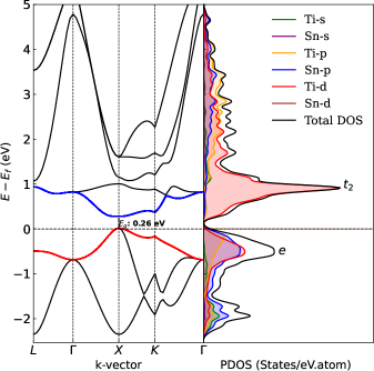
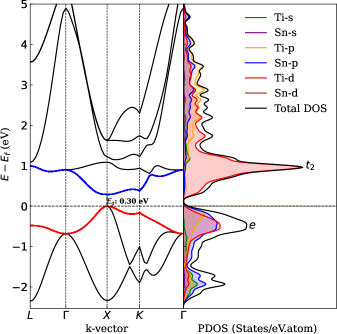
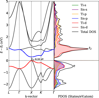
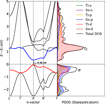
The ground state electronic band structure of zb-TiSn exhibits a direct and narrow band gap at high symmetry point ‘X’ in the Brillioun zone. This direct band gap effectively supports the transition of optically generated electrons, greatly increasing the rate of electronic transitions[35]. To investigate the contributions of atomic states near the Fermi surface, the energy axis is set from -2.5 eV to +5 eV. The projected density of states (PDOS) reveals that the Ti d-states, Ti p-states, and Sn p-states contribute significantly in this region. This indicates that electrons from these Ti d-state, Ti p-state and Sn p-state are more likely to transition to the conduction band minimum and play a crucial role in determining the electronic properties of zinc blende Ti-Sn [36].
It is evident from the projected density of states that the valence band is comprised of Ti-3d states and Sn-5p states, resulting from of p-d hybridization. In tetrahedral coordination of zb-TiSn, the five -orbitals of Ti will split into two sets due to the electrostatic field from four Sn-ligands positioned at the corners of a tetrahedron. The orbitals experience more repulsion as they point closer to the ligand directions, making them higher in energy, while the orbitals point between ligands and are lower in energy. Since the orbitals are lower in energy in tetrahedral coordination, electrons fill them first according to the Aufbau principle. These occupied low-energy states contribute to the valence band. In contrast, the orbitals are higher in energy and partially occupied, contributing mainly to the conduction band as available excited states.
| Band gap(eV) | |
|---|---|
| LDA-PZ | 0.26 eV |
| GGA-PBE | 0.30 eV |
| GGA-RPBE | 0.32 eV |
| GLLB-sc | 0.38 eV |
Based on the nature of the exchange and correlation functionals, the estimated band gap is listed in Table 2. zb-TiSn exhibits relatively small band gap of 0.26 eV with LDA-PZ, 0.30 eV with GGA-PBE and 0.32 eV with GGA-RPBE functionals.To assess the robustness of the electronic structure, calculations were performed using the GLLB-sc functional, which incorporates a derivative discontinuity correction which is absent in ordinary GGA and LDA functionals. The converged lattice constant was found to be 6.215 Å, and the calculated band gap was 0.38 eV. This band gap is in qualitative agreement with band gap values obtained from LDA-PZ, GGA-PBE, and GGA-RPBE functionals and supports that fact that zb-TiSn could be a narrow band gap semiconductor. Further, we have used GGA-PBE+U method to study the effect of Hubbard ‘U’ correction on the lattice parameter and the resulting band gap. However, the results indicated that the band gap appeared to be very similar across the entire U range, suggesting that the effect of Hubbard U correction on the band gap energy is marginal in zb-TiSn.
3.3 Effective mass
Effective mass is an important material parameter that governs most of the carrier transport properties in semiconductors. Precise knowledge of effective mass is important for the design technology of optoelectronic devices[37]. Since the effective mass directly influences the mobility of charge carriers, it plays a significant role in determining the performance and efficiency of these devices.
The effective mass is calculated using the expression[38]
| (2) |
By fitting the actual dispersion curve around conduction band minima (CBM) and valance band maxima (VBM) of energy eigenvalues, the effective mass of electrons and holes can be obtained. We have used the -order polynomial fit as the band extrema in zb-TiSn are appearing not strictly parabolic and hence we have used the following expression to fit the dispersion curve.
| (3) |
The first and second-order differentiation of equation 3 with respect to momentum space gives
| (4) |
and
| (5) |
Thus, the effective mass can be obtained as
| (6) |
Where is the effective mass and , , and are the coefficients of the polynomials used for curve fitting.
Since the effective mass is related to the curvature of the band extrema, setting the first derivative of E(k) to zero and solving the resulting cubic polynomial equation identifies the extrema (critical points) of the electronic band structure. The effective mass of electrons and holes for TiSn are calculated by fitting the preuso-parabolic curves at CBM and VBM in the band structure of TiSn located at high symmetry point ‘X’ of the Brillouin zone. With different exchange correlation functions, namely LDA-PZ, GGA-PBE, and GGA-RPBE, the calculated effective mass are tabulated in Table 3.
| Conduction Band | Valence Band | |
|---|---|---|
| (-X-K) | (-X-K) | |
| LDA-PZ | ||
| GGA-PBE | ||
| GGA-RPBE |
At the high-symmetry point ‘X’, the effective mass of charge carriers at the CBM is significantly larger than that at the VBM due to the flatness of the CBM. The lower effective mass at the VBM facilitates the excitation of charge carriers to the CBM. However, the higher effective mass at the CBM restricts their mobility, causing them to remain localized. This localization of charge carriers at the CBM results in minimal dispersion, making electrons appear much heavier. This significantly reduces their kinetic energy, which causes electron interactions to dominate and giving rise to interesting physical phenomenon such as fractional quantum Hall effect[39, 40], Wigner crystallization[41], Bose-Einstein condensation[42], and high-temperature superconductivity[43, 44].
3.4 Charge density distribution
In DFT, the electron density describes the distribution of electrons in a material, providing insights into bonding characteristics. Using GPAW, the charge density is obtained by solving the self-consistent Kohn-Sham equations[45]. The charge density is then reconstructed from the occupied Kohn-Sham orbitals using the equation 7,
| (7) |
Where, is Kohn-Sham wave function, is occupation number from Fermi-Dirac distribution and represents the probability density.
The nature of the chemical bond between two atoms can be determined by the difference in their electronegativity values. According to the Pauling scale, the electronegativity values for Ti is 1.54[46] and Sn it is 1.91[47] and their electronegativity difference is for the Ti-Sn bond. When the electronegativity difference is , that would indicate covalent nature of the bond [48]. With 0.42 as the electronegativity difference, Ti-Sn bond appears to be covalent as all other zincblende structured compounds.
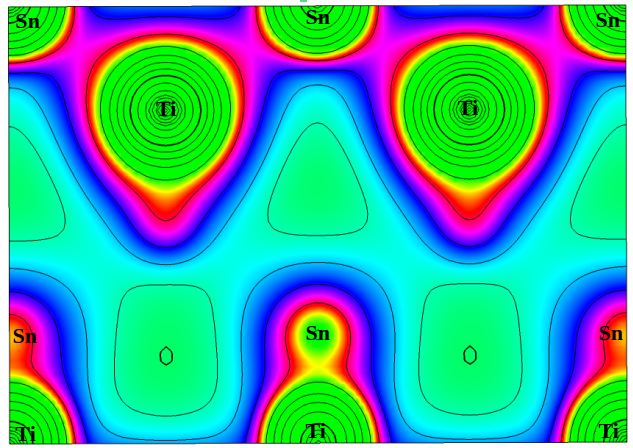
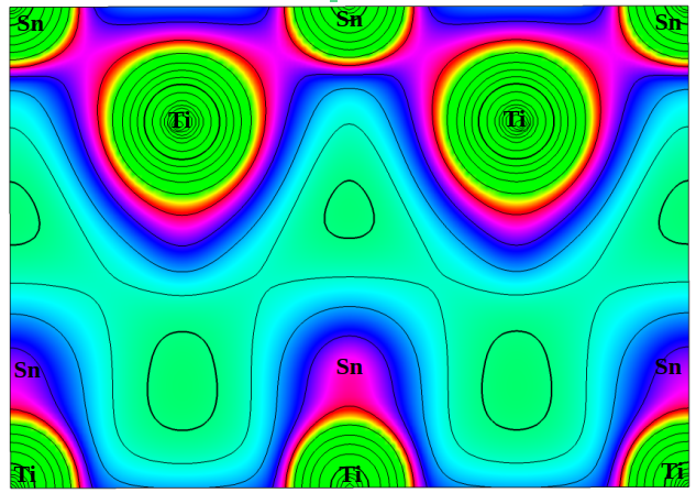
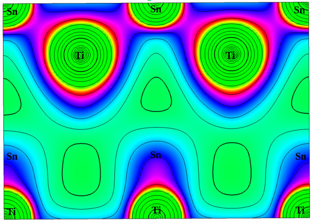
Along the (1 1 0) crystallographic plane, with projection range of LDA-PZ(3.8-6 e/Å3), GGA-PBE(3.8-6.2 e/Å3), and GGA-RPBE(3.8-6.3 e/Å3), the electron density plots of zb-TiSn are shown in Figure2 a,b and c. The extended charge distribution of the denser electron cloud from Ti to Sn suggests covalent bonding, which results from p-d hybridization, as evidenced in the PDOS shown in Figure 1. Observing the charge density plots reveals that the bonds between Ti and Sn is predominantly covalent and with certain degree of ionic character.
From Figure 2 a, b and c, it is evident that, the exchange and correlation functionals has distinct effect on charge distribution. In the Figure 2a, we show the charge density plot calculated with LDA-PZ. The contours are more tightly packed around the atoms Ti and Sn suggesting stronger localization of electrons. The bonding regions (between atoms) show less charge delocalization. With GGA-PBE in Figure 2b, the charge density is more smeared out, particularly in the bonding regions. The contours are slightly more diffuse compared to LDA-PZ, indicating reduced localization. Additionally, the outer contours are exhibiting a small distortion from their regular circular shape and extend into interstitial regions (seen more in GGA-PBE), suggesting that the charge is spreading due to hybridization between Ti and Sn atoms.
Based on the color code we could interpret the charge density plots as follows. Green representing the high charge density which is evident around atomic cores of Ti and Sn, indicating localized electron density. Red/Purple is representing the intermediate or medium density signifying the bonding regions where charge accumulates. Blue/Cyan represents the low charge density regions indicating the charge depletion with low electron density. The interstitial regions, where charges will get depleted and no charge contours can be observed. In LDA-PZ as shown in Figure2 a, no charge contours because of higher localization and in GGA-RPBE (Figure2 c), the charge density has been depicted as slowly varying between the atoms signifying the covalent nature of the bond. However, GGA-PBE suggests that the bond can be polar covalent. This discrepancy can be clarified by quantifying the amount of charge which has been shared or transferred using Bader charge analysis.
3.5 Bader Charge Analysis
In a crystal, electrons are shared between atoms, making it difficult to define atomic charge and the amount of charge transfer. The Bader method[49][50][51] solves this by partitioning the electron density of the total space into separate basins (regions), where each basin corresponds to an individual atom, called atomic basin.
Comparing the total number of electrons in the atomic basin of an atom with its neutral atom reveals the amount of charge transfer. Using Bader charge analysis, the amount of charge transfer between Ti and Sn in the zincblende structure under LDA-PZ, GGA-PBE, and GGA-RPBE functionals is computed and tabulated in Table 4.
| Functional | Titanium (Ti) Charge (e) | Tin (Sn) Charge (e) |
|---|---|---|
| LDA-PZ | -1.05 | 1.05 |
| GGA-PBE | -1.11 | 1.11 |
| GGA-RPBE | -1.14 | 1.14 |
Bader charge analysis sheds light on zb-TiSn bonding behavior, showing that Ti loses and Sn gains in LDA-PZ, while in GGA-PBE, Ti loses and Sn gains and the GGA-RPBE values are similar for Ti and Sn as shown in the table 4. Charge transfer in TiSn creates a partial negative charge on Sn and a partial positive charge on Ti, confirming the polar covalent nature of the Ti-Sn bond.
4 Lattice dynamics of zb-TiSn
Since the compound zb-TiSn has not been realised experimentally, we aim to establish the compound’s phase stability via lattice dynamics. We have calculated the phonon dispersion along the high symmetry points spanning the entire Brillioun zone. Using DFPT method, we have computed the dynamic matrices and extracted the inter atomic force constants.
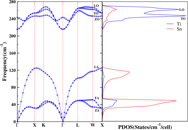
Zincblende TiSn belongs to the point group Td(43m) and has two atoms per primitive cell, yielding six phonon branches; one longitudinal acoustic (LA), two transverse acoustic (TA and ZA), one longitudinal optic (LO), and two transverse optic (TO and ZO) modes. The optical phonons exhibits symmetry, consisting of one LO mode and two doubly degenerate TO modes. Around the point, the transverse acoustic (TA) and longitudinal acoustic (LA) modes exhibit linear behavior, providing insights into the velocity of sound and thermal conductivity[52] of the material.
The degeneracy of the optical modes vanishes in both LDA-PZ and GGA-PBE at the point, resulting in LO-TO splitting attributed to the Lyddane–Sachs–Teller (LST) phenomenon[53], as shown in Figure 3 a and b. The LO-TO splitting arises from long-range Coulomb interactions in polar materials, leading to different vibrational frequencies for longitudinal and transverse optical modes at the point. The LO modes exhibits higher energy than the TO modes due to partial ionic bonding arising from long-range Coulomb interactions, which can be described using Born effective charge tensors[54].
The Born effective charge tensors and were found to be diagonal, with only a single distinct component due to high symmetry. In GGA-PBE, the Born effective charges (in the units of elementary charge) are 3.98 for Ti and -3.98 for Sn, whereas in LDA-PZ, they are slightly higher at 4.56 for Ti and -4.51 for Sn. These values, which are significantly larger than the nominal ionic charges, indicate strong charge transfer and polarization, leading to a stronger response of Ti and Sn atoms to external electric fields. The deviation of the Born effective charges from their nominal values highlights the mixed ionic-covalent nature of TiSn, where Ti donates charge while Sn accepts it. LDA-PZ predicts higher Born effective charges due to its smaller lattice constant, which strengthens atomic interactions and enhances charge transfer. Conversely, GGA-PBE, with its larger lattice constant, weakens these interactions, leading to lower Born effective charges and reduced charge polarization.
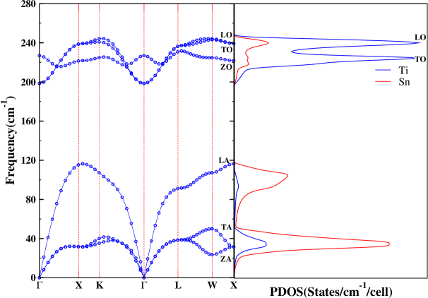
LO-TO splitting arises from the ionic component in polar and covalent bonds. It is evident in the charge density difference plot of zb-TiSn, which reveals that the charge accumulation zones on Sn atoms and depletion zones on Ti. The interaction between lattice vibrations and polarization, caused by out-of-phase atomic vibrations in ionic or polar crystals, explains the LO-TO splitting. This phenomenon occurs only in optical phonons, which arise when the cation Ti and anion Sn vibrate in opposite directions, creating an oscillating dipole. Long-range dipole–dipole interactions significantly impact the optical branches, causing the longitudinal and transverse optical modes to split more near the -point.
The phonon spectra obtained from both GGA-PBE and LDA-PZ are comparable, as seen in the phonon density of states (PDOS), where the LO, TO, LA, and TA branches are clearly distinguishable. The optical branches, particularly the longitudinal ones, remain flat due to the mass mismatch between Ti and Sn. As a result, the acoustic and optical branches are separated by a phonon gap appearing between 124 to 215 cm-1 in LDA-PZ and 116 to 198 cm-1 in GGA-PBE. Although experimental data for TiSn are unavailable, the computed optical phonon spectra closely resembles those reported for a similar zincblende compounds, such as ZnSe [55]. To further investigate the LO-TO splitting in TiSn, the screened effective charges were calculated using both LDA-PZ and GGA-PBE functionals:
| (8) |
In LDA-PZ, the Born effective charge of Ti is and the long wavelength dielectric constant is , yielding a screened effective charge () of 0.721, while in GGA-PBE, with Born effective charge of Ti, and , resulting in . The computed screened effective charges suggest that zb-TiSn behaves similar to the established zincblende semiconductors, such as ZnO (), ZnS (), ZnSe (), and ZnTe ()[55].
In zb-TiSn, the longitudinal optical (LO) phonon frequency is higher than the transverse optical (TO) phonon frequency at the X symmetry point. At this q point, the heavier atom (Sn) primarily participate in the LA phonon mode, while the lighter atom (Ti) vibrates with the LO phonon mode. The calculated frequency ratio is for GGA-PBE and for LDA-PZ closely matches the square root mass ratio , or approximately . Minor discrepancies arise due to LDA-PZ tendency to overestimate and GGA-PBE’s tendency to underestimate phonon frequencies.
According to Srivastava et al.,[56] the hypothesis that any zincblende (ZB) or rock-salt material with a mass ratio greater than two would satisfy the condition holds true for TiSn, reinforcing its lattice dynamics consistent with other zincblende compounds.
The phonon density of states (PDOS) provides insight into the vibrational properties of the constituent atoms. The low-frequency region, ranging from approximately zero to cm-1 in LDA-PZ and zero to cm-1 in GGA-PBE, corresponds to acoustic phonon modes dominated by Sn vibrations. Due to the mass difference, the lighter Ti atoms exhibits higher vibrational frequencies, leading to higher optical phonon frequencies.
5 Optical Properties
Studying the optical properties of narrow band gap semiconductors is crucial for optimizing their performance for various applications, such as photo-detectors, solar cells, and infrared sensors. Understanding how these materials interact with light will enable the design of devices with improved efficiency and reduced energy losses.
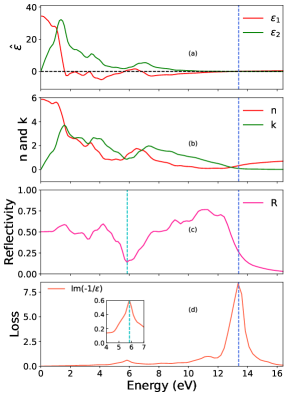
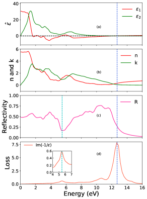
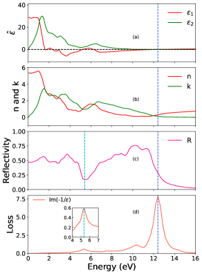
We analyze the linear optical properties of zb-TiSn including the refractive index ‘n’, extinction coefficient ‘k’, reflectivity ‘R’ of zb-TiSn. These optical properties of TiSn are studied through the dielectric function, which describes the linear response of the system to light. Within the Random Phase Approximation (RPA) , the dielectric function is derived from the electronic band structure, calculated using LDA-PZ, GGA-PBE and GGA-RPBE approximation as shown in Figure4a,b and c. However, we have extended out calculations using GLLB-sc functional also which could determine the band gap energy accurately compared to the functional mentioned before. The resulting band gap from GLLB-sc is 0.38 eV and it is very similar to the one obtained using GGA-PBE and GGA-RPBE. Hence we have chosen not to present the optical properties from GLLB-sc in the manuscript, however we have provide them in the section-8 of the supplementary data file for readers convenience.
The dielectric function , describes the optical response of the medium as a function of frequency . Where, the real part of the dielectric function represents polarization response of the material to the incident light, describing the the non-dissipative ”screening” effect that influences the light propagation through the material. In contrast, the imaginary part corresponds to the dissipative response of electrons to incoming electromagnetic waves, leading to energy loss as the wave propagates through the material. The expression for the imaginary part of the dielectric function is given by[57]
| (9) |
where, is the dipole matrix, and represent the initial and final states respectively, the Fermi distribution function for the -th state, and is the energy of electron in the -th state with crystal wave vector .
| (10) |
| (11) |
where denotes the principal value of the integral.
The reflectivity of solids at normal incidence is given by Fresnel’s relation:
| (12) |
where the refractive index and extinction coefficient are:
| (13) |
| (14) |
From Drude model the energy loss spectrum is given by,
| (15) |
As shown in figure 4a, the real part of the dielectric function exhibits normal dispersion until 1.08 eV after which it undergoes anomalous dispersion, indicating the small band gap and high refractive index of the material. The refractive index (LDA-PZ),5.52 (GGA-PBE) and 5.35 (GGA-RPBE) initially marks high polarizability as shown in figure 4b. crosses zero at 1.62 eV and remains below zero until 5.66 eV further supporting the small band gap nature of the zb-TiSn. The effect of GGA-PBE and GGA-RPBE is relatively less on the linear optical properties and they appear similar to LDA-PZ. The imaginary part of the dielectric function reaches a peak maxima at 1.34 eV marking the inflection point in as shown in figure 4a.
The reflectivity curve of the zb-TiSn semiconductor is shown in Figure 4c. The reflectivity reaches an average of 50% in the infrared and visible regions, with a maximum of 76% at 11.06 eV(LDA-PZ),10.43 eV (GGA-PBE) and 10.26 eV(GGA-RPBE). The short valley at 5.87 eV (LDA-PZ),5.43 eV(GGA-PBE)and 5.36 eV (GGA-RPBE) corresponds to the surface plasmon frequency, while the peak at 16.31 eV(LDA-PZ),16.80(GGA-PBE) and 15.50 eV(GGA-RPBE) marks the volume plasmon frequency. The plasmon frequencies are distinctly visible in the loss spectra as shown in figure 4d. By tailoring the optical characteristics of narrow band gap semiconductors, photon capture can be enhanced, optical losses in waveguides can be minimized and more efficient optoelectronic devices can be designed and developed, particularly for infrared and near-infrared applications.
Light absorption is a key factor in determining the properties like photovoltaic and photocatalytic efficiency[60], we have calculated the absorption coefficient of zb-TiSn with PBE functional, the absorption coefficient is given by [61]
| (16) |
Where is light velocity, is the refraction index:
| (17) |
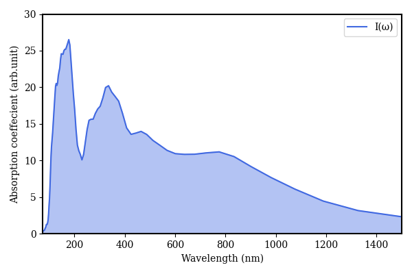
The absorption spectrum using GGA-PBE is shown in Figure 5, marks effective absorption from 100 to 1500 nm, covering the ultraviolet (UV), visible (VIS), and near- infrared (NIR) regions.These results indicate that zb-TiSn is highly effective in absorbing radiation within this range. The transition of the generated free charge carriers are driven by the energy absorbed from the entire energy range of 100 to 1500 nm, supporting efficient optoelectronic performance, particularly in applications like low-energy photodetectors for infrared region and waste heat harvesting.(For the absorption spectra of other functionals, please refer section-9 in the supplementary data file )
6 Conclusion
Through first-principles calculations based on density functional theory, we have investigated the zincblende structure of TiSn and identified it as a narrow bandgap semiconductor based on its electronic band structure. The structural properties were determined by optimizing the energy eigenvalues and fitting them to the Murnaghan equation of state to extract the lattice constant, equilibrium volume, bulk modulus, and its derivative for the ground state of zb-TiSn. The electronic band structure was computed along the high-symmetry path (L--X-K-) of the Brillouin zone, and the carrier effective mass near the conduction band minimum (CBM) and valence band maximum (VBM) was determined. The charge density distribution plot indicates the presence of covalent bonding through charge sharing, while Bader charge analysis provides evidence of ionic bonding by measuring charge transfer. The optical properties of zb-TiSn were analyzed using the complex dielectric function and Kramers-Kronig relations, revealing its sensitivity to infrared (IR) radiation. All calculations were performed using three different exchange-correlation functionals, LDA-PZ, GGA-PBE, and GGA-RPBE to assess the robustness of the semiconductor material.
Conflicts of interest
There are no conflicts to declare.
Acknowledgements
SR,SM and UMKK would like to thank Mr.Mohan Kumar C M(Deputy Director-CTS-VIT) for providing us with computational resources. The authors acknowledge VIT SEEDGRANT-SG20240040supporting the current research project.
Author contributions
Sudeep R contributed to DFT calculations for electronic structure, Investigation, Visualization and first draft preparation; Sarojini M also equally contributed to DFT calculations for lattice dynamics, Investigation, Visualization and first draft preparation; Uma Mahendra Kumar K: Conceptualization, Methodology, Visualization, Investigation and Writing- Reviewing and Editing.
References
- [1] A. Castellanos-Gomez, Black phosphorus: narrow gap, wide applications, The journal of physical chemistry letters 6 (21) (2015) 4280–4291. doi:https://doi.org/10.1021/acs.jpclett.5b01686.
- [2] I. T. Witting, T. C. Chasapis, F. Ricci, M. Peters, N. A. Heinz, G. Hautier, G. J. Snyder, The thermoelectric properties of bismuth telluride, Advanced Electronic Materials 5 (6) (2019) 1800904. doi:https://doi.org/10.1002/aelm.201800904.
- [3] J. P. Heremans, V. Jovovic, E. S. Toberer, A. Saramat, K. Kurosaki, A. Charoenphakdee, S. Yamanaka, G. J. Snyder, Enhancement of thermoelectric efficiency in pbte by distortion of the electronic density of states, Science 321 (5888) (2008) 554–557. doi:10.1126/science.1159725.
- [4] A. Boyer, E. Cisse, Y. Azzouz, J. Cheron, Narrow-bandgap semiconductor-based thermal sensors, Sensors and Actuators A: Physical 27 (1-3) (1991) 637–640. doi:https://doi.org/10.1016/0924-4247(91)87063-9.
- [5] R. Q. Yang, W. Huang, M. B. Santos, Narrow bandgap photovoltaic cells, Solar Energy Materials and Solar Cells 238 (2022) 111636. doi:https://doi.org/10.1016/j.solmat.2022.111636.
- [6] N. Dai, Optoelectronic properties of narrow band gap semiconductors, De Gruyter, Berlin, München, Boston, 2015, pp. 1–50. doi:doi:10.1515/9783110307023.1.
- [7] J. Chu, A. Sher, Physics and properties of narrow gap semiconductors, Springer New York, NY, Berlin, Heidelberg, 2008. doi:https://doi.org/10.1007/978-0-387-74801-6.
- [8] A. Rogalski, P. Martyniuk, M. Kopytko, P. Madejczyk, S. Krishna, Inassb-based infrared photodetectors: Thirty years later on, Sensors 20 (24) (2020) 7047. doi:https://doi.org/10.3390/s20247047.
- [9] M. Berding, S. Krishnamurthy, A. Sher, A.-B. Chen, Electronic and transport properties of hgcdte and hgznte, Journal of Vacuum Science & Technology A: Vacuum, Surfaces, and Films 5 (5) (1987) 3014–3018. doi:https://doi.org/10.1116/1.574249.
- [10] A. Rogalski, Hgcdte infrared detector material: history, status and outlook, Reports on Progress in Physics 68 (10) (2005) 2267. doi:10.1088/0034-4885/68/10/R01.
- [11] M. B. Reine, Hgcdte photodiodes for ir detection: a review, Photodetectors: Materials and Devices VI 4288 (2001) 266–277. doi:https://doi.org/10.1117/12.429413.
- [12] X.-H. Li, Y.-X. Guo, Y. Ren, J.-J. Peng, J.-S. Liu, C. Wang, H. Zhang, Narrow-bandgap materials for optoelectronics applications, Frontiers of Physics 17 (2022) 1–33. doi:https://doi.org/10.1007/s11467-021-1055-z.
- [13] T. B. MASSALSKI, Binary alloy phase diagrams, ASM International 3 (1990) 2271–2273.
-
[14]
J. L. MURRAY, Phase
diagram of titanium alloys, ASM International 182 (1987).
URL https://cir.nii.ac.jp/crid/1570854174084521472 - [15] F. H. Hayes, P. J. Horrocks, Thermodynamic database for light metal alloys, in: I. Ansara, A. T. Dinsdale, M. H. Rand (Eds.), COST 507, Vol. 2, Office for Official Publications of the European Communities, Luxembourg, 1998, pp. 284–287. doi:https://doi.org/10.1007/b76778.
- [16] F. H. Hayes, Binary systems from Mn–Mo to Y–Zr, in: Landolt-Börnstein - Group IV Physical Chemistry, Vol. 19B4, Springer, Berlin, Heidelberg, 2006, pp. 1–4.
- [17] C. Kuper, W. Peng, A. Pisch, F. Goesmann, R. Schmid-Fetzer, Phase formation and reaction kinetics in the system ti-sn, Z. Metallkd. 89 (12) (1998) 855–862. doi:https;//doi.org/10.3139/ijmr-1998-0165.
- [18] J. H. N. van Vucht, H. A. C. M. Bruning, H. C. Donkersloot, A. H. G. de Mesquita, The system vanadium-gallium, Philips Res. Rep. 19 (5) (1964) 407–421.
- [19] C. Colinet, J.-C. Tedenac, S. G. Fries, Structural stability of intermetallic phases in the sn–ti system, Calphad 33 (1) (2009) 250–259. doi:https://doi.org/10.1016/j.calphad.2008.08.001.
-
[20]
S. Kirklin, J. E. Saal, B. Meredig, A. Thompson, J. W. Doak, M. Aykol,
S. Rühl, C. Wolverton,
The open quantum
materials database (oqmd): assessing the accuracy of dft formation energies,
npj Computational Materials 1 (1) (2015) 15010.
doi:10.1038/npjcompumats.2015.10.
URL https://doi.org/10.1038/npjcompumats.2015.10 -
[21]
M. Mizuguchi, H. Akinaga, T. Manago, K. Ono, M. Oshima, M. Shirai, M. Yuri,
H. J. Lin, H. H. Hsieh, C. T. Chen,
Epitaxial growth of zinc-blende
cras/gaas multilayer, Journal of Applied Physics 91 (10) (2002) 7917–7919.
arXiv:https://pubs.aip.org/aip/jap/article-pdf/91/10/7917/18978621/7917\_1\_online.pdf,
doi:10.1063/1.1455612.
URL https://doi.org/10.1063/1.1455612 - [22] O. Chichvarina, T. S. Herng, K. C. Phuah, et al., Stable zinc-blende zno thin films: formation and physical properties, Journal of Materials Science 50 (2015) 28–33. doi:https://doi.org/10.1007/s10853-014-8561-0.
- [23] N. Li, et al., Growth and stress-induced transformation of zinc blende aln layers in al-aln-tin multilayers, Scientific Reports 5 (2015) 18554. doi:https://doi.org/10.1038/srep18554.
- [24] A. KrAl, P. Pomastowski, K. RafiAska, V. Railean-Plugaru, B. Buszewski, Zinc oxide nanoparticles: Synthesis, antiseptic activity and toxicity mechanism, Advances in colloid and interface science 249 (2017) 37–52. doi:https://doi.org/10.1016/j.cis.2017.07.033.
- [25] Y. Ding, X. D. Wang, Z. L. Wang, Phase controlled synthesis of zns nanobelts: zinc blende vs wurtzite, Chemical physics letters 398 (1-3) (2004) 32–36. doi:https://doi.org/10.1016/j.cplett.2004.09.031.
- [26] M. Alrefaee, U. P. Singh, S. K. Das, Growth of aluminum doped zinc oxide nanostructure thin films by nonconventional sol-gel method 402 (1) (2022) 2100350. doi:https://doi.org/10.1002/masy.202100350.
-
[27]
S. Manickavasagam, U. M. K. Koppolu,
First-principle
investigation of zb-tige: A promising narrow bandgap semiconductor, physica
status solidi (b) 262 (2) (2025) 2400475.
doi:https://doi.org/10.1002/pssb.202400475.
URL https://onlinelibrary.wiley.com/doi/abs/10.1002/pssb.202400475 - [28] J. J. Mortensen, A. H. Larsen, M. Kuisma, A. V. Ivanov, A. Taghizadeh, A. Peterson, A. Haldar, A. O. Dohn, C. Schäfer, E. Ö. Jónsson, et al., Gpaw: An open python package for electronic structure calculations, The Journal of Chemical Physics 160 (9) (2024). doi:https://doi.org/10.1063/5.0182685.
- [29] D. M. Ceperley, B. J. Alder, Ground state of the electron gas by a stochastic method, Physical review letters 45 (7) (1980) 566. doi:https://doi.org/10.1103/PhysRevLett.45.566.
- [30] J. P. Perdew, K. Burke, M. Ernzerhof, Generalized gradient approximation made simple, Physical review letters 77 (18) (1996) 3865. doi:https://doi.org/10.1103/PhysRevLett.77.3865.
- [31] B. Hammer, L. B. Hansen, J. K. Nørskov, Improved adsorption energetics within density-functional theory using revised perdew-burke-ernzerhof functionals, Physical review B 59 (11) (1999) 7413. doi:https://doi.org/10.1103/PhysRevB.59.7413.
- [32] A. H. Larsen, J. J. Mortensen, J. Blomqvist, I. E. Castelli, R. Christensen, M. Dułak, J. Friis, M. N. Groves, B. Hammer, C. Hargus, et al., The atomic simulation environment—a python library for working with atoms, Journal of Physics: Condensed Matter 29 (27) (2017) 273002. doi:https://doi.10.1088/1361-648X/aa680e.
- [33] S. Gražulis, D. Chateigner, R. T. Downs, A. Yokochi, M. Quirós, L. Lutterotti, E. Manakova, J. Butkus, P. Moeck, A. Le Bail, Crystallography open database–an open-access collection of crystal structures, Applied Crystallography 42 (4) (2009) 726–729. doi:https://doi.org/10.1107/S0021889809016690.
- [34] F. D. Murnaghan, The compressibility of media under extreme pressures, Proceedings of the National Academy of Sciences 30 (9) (1944) 244–247. doi:https://doi.org/10.1073/pnas.30.9.244.
- [35] D. Fan, M. Yin, K. Wang, Z. Wang, H. Li, H. Hu, F. Guo, Z. Feng, J. Li, D. Zhang, et al., The transition from indirect band gap to direct band gap and effectively separating of electron-hole pairs in h-bc2n/mosi2n4 heterojunction for photocatalytic water splitting, International Journal of Hydrogen Energy 107 (2025) 452–459. doi:https://doi.org/10.1016/j.ijhydene.2024.05.442.
- [36] M. Yin, D. Fan, Z. Wang, H. Li, H. Hu, F. Guo, Z. Feng, J. Li, D. Zhang, M. Zhu, et al., The absorption of transition metal atoms in g-c6n6 nanoribbon induces narrow band gap semiconductor with magnetism, Physica B: Condensed Matter 667 (2023) 415158. doi:https://doi.org/10.1016/j.physb.2023.415158.
- [37] M. Dyksik, H. Duim, X. Zhu, Z. Yang, M. Gen, Y. Kohama, S. Adjokatse, D. K. Maude, M. A. Loi, D. A. Egger, et al., Broad tunability of carrier effective masses in two-dimensional halide perovskites, ACS Energy Letters 5 (11) (2020) 3609–3616. doi:https://doi.org/10.1021/acsenergylett.0c01758.
- [38] C. Kittel, P. McEuen, Introduction to solid state physics, John Wiley & Sons, Newyork, 2018.
- [39] E. Tang, J.-W. Mei, X.-G. Wen, High-temperature fractional quantum hall states, Physical review letters 106 (23) (2011) 236802. doi:https://doi.org/10.1103/PhysRevLett.106.236802.
- [40] K. Sun, Z. Gu, H. Katsura, S. Das Sarma, Nearly flatbands with nontrivial topology, Physical review letters 106 (23) (2011) 236803. doi:https://doi.org/10.1103/PhysRevLett.106.236803.
- [41] C. Wu, D. Bergman, L. Balents, S. Das Sarma, Flat bands and wigner crystallization in the honeycomb optical lattice, Physical review letters 99 (7) (2007) 070401. doi:https://doi.org/10.1103/PhysRevLett.99.070401.
- [42] S. D. Huber, E. Altman, Bose condensation in flat bands, Physical Review B—Condensed Matter and Materials Physics 82 (18) (2010) 184502. doi:https://doi.org/10.1103/PhysRevB.82.184502.
- [43] M. Imada, M. Kohno, Superconductivity from flat dispersion designed in doped mott insulators, Physical Review Letters 84 (1) (2000) 143. doi:https://doi.org/10.1103/PhysRevLett.84.143.
- [44] S. Peotta, P. Törmä, Superfluidity in topologically nontrivial flat bands, Nature communications 6 (1) (2015) 8944. doi:https://doi.org/10.1038/ncomms9944.
- [45] W. Kohn, L. J. Sham, Self-consistent equations including exchange and correlation effects, Physical review 140 (4A) (1965) A1133. doi:https://doi.org/10.1103/PhysRev.140.A1133.
- [46] M. Ito, D. Setoyama, J. Matsunaga, H. Muta, K. Kurosaki, M. Uno, S. Yamanaka, Effect of electronegativity on the mechanical properties of metal hydrides with a fluorite structure, Journal of alloys and compounds 426 (1-2) (2006) 67–71. doi:https://doi.org/10.1016/j.jallcom.2006.02.036.
- [47] K. T. Giju, F. De Proft, P. Geerlings, Comprehensive study of density functional theory based properties for group 14 atoms and functional groups,- xy3 (x= c, si, ge, sn, pb, element 114; y= ch3, h, f, cl, br, i, at), The Journal of Physical Chemistry A 109 (12) (2005) 2925–2936. doi:https://doi.org/10.1021/jp050463x.
- [48] G. Sproul, Electronegativity and bond type: Predicting bond type, Journal of Chemical Education 78 (3) (2001) 387. doi:https://doi.org/10.1021/ed078p387.
- [49] G. Henkelman, A. Arnaldsson, H. Jónsson, A fast and robust algorithm for bader decomposition of charge density, Computational Materials Science 36 (3) (2006) 354–360. doi:https://doi.org/10.1016/j.commatsci.2005.04.010.
- [50] E. Sanville, S. D. Kenny, R. Smith, G. Henkelman, Improved grid-based algorithm for bader charge allocation, Journal of computational chemistry 28 (5) (2007) 899–908. doi:https://doi.org/10.1002/jcc.20575.
- [51] W. Tang, E. Sanville, G. Henkelman, A grid-based bader analysis algorithm without lattice bias, Journal of Physics: Condensed Matter 21 (8) (2009) 084204. doi:https://10.1088/0953-8984/21/8/084204.
-
[52]
N. W. Ashcroft, N. D. Mermin, Solid
state physics, Holt, Rinehart and Winston, New York, NY, 1976.
URL https://cds.cern.ch/record/102652 - [53] R. H. Lyddane, R. Sachs, E. Teller, On the polar vibrations of alkali halides, Physical Review 59 (8) (1941) 673. doi:https://doi.org/10.1103/PhysRev.59.673.
- [54] X. Gonze, C. Lee, Dynamical matrices, born effective charges, dielectric permittivity tensors, and interatomic force constants from density-functional perturbation theory, Physical Review B 55 (16) (1997) 10355. doi:https://doi.org/10.1103/PhysRevB.55.10355.
- [55] Y. Yu, J. Zhou, H. Han, C. Zhang, T. Cai, C. Song, T. Gao, Ab initio study of structural, dielectric, and dynamical properties of zinc-blende znx (x= o, s, se, te), Journal of alloys and compounds 471 (1-2) (2009) 492–497. doi:https://doi.org/10.1016/j.jallcom.2008.04.039.
- [56] G. Srivastava, H. Tütüncü, N. Günhan, First-principles studies of structural, electronic, and dynamical properties of be chalcogenides, Physical Review B—Condensed Matter and Materials Physics 70 (8) (2004) 085206. doi:https://doi.org/10.1103/PhysRevB.70.085206.
- [57] N. V. Smith, Photoelectron energy spectra and the band structures of the noble metals, Physical Review B 3 (6) (1971) 1862. doi:https://doi.org/10.1103/PhysRevB.3.1862.
- [58] F. Wooten, Optical properties of solids, Academic Press: New York, NY, USA; London, UK, 1972. doi:https://doi.org/10.1016/C2013-0-07656-6.
- [59] U. M. K. Koppolu, Electronic band structure and complex dielectric function of zb-alp: a first principles study, Acta Phys Polonica A 136 (3) (2019) 486–489. doi:https://doi.org/10.12693/APhysPolA.136.486.
- [60] X. Hu, H. Li, H. Hu, C. Bai, C. Liu, F. Guo, Z. Feng, J. Li, D. Fan, Z. Wang, A potential application of a crystal triazine organic framework in energy: Photocatalytic decomposition of water, Physica B: Condensed Matter 623 (2021) 413342. doi:https://doi.org/10.1016/j.physb.2021.413342.
- [61] S. Guan, Y. Cheng, C. Liu, J. Han, Y. Lu, S. A. Yang, Y. Yao, Effects of strain on electronic and optic properties of holey two-dimensional c2n crystals, Applied Physics Letters 107 (23) (2015). doi:https://doi.org/10.1063/1.4937269.