Imaging domain boundaries of rubrene thin crystallites by photoemission electron microscopy
The progress of designing organic semiconductors is extensively dependent on the quality of prepared organic molecular assemblies, since the charge transport mechanism is strongly efficient in highly ordered crystals compared to amorphous domains. Here we present a comprehensive photoemission electron microscopy (PEEM) and time-of-flight (TOF) spectroscopic study of rubrene () thin crystals focusing on recently developed orthorhombic crystalline morphologies applied in organic electronic devices. Using femtosecond pulsed lasers with photon energies between 3–6 eV, we explore the interplay between photoemission processes, crystal morphology, and defect states. In a 2-photon photoemission process (2PPE), the PEEM images reveal dominant emission localized at domain boundaries, indicating strong contributions from trap states. In contrast, in 1PPE nm excitation uniform emission across the crystal surface is observed, highlighting a fundamental difference in photoemission mechanisms. Furthermore, in the intermediate photon energy range, we identify a nonlinear, non-integer photon order, where mostly the triclinic morphology contributes to the emission, distinguishing it from the orthorhombic phase. These findings provide a new framework for assessing the quality and internal structure of organic semiconductor thin films via wavelength-dependent photoemission imaging and spectroscopy.
1 Introduction
Organic semiconducting molecules have attracted a lot of attention in the recent decades due to their promising charge transport properties. Among all the organic molecules, rubrene () offers one of the highest charge carrier mobilities [1, 2]. This charge mobility is associated with a process known as singlet fission [3, 4]. Singlet fission is the transformation of an excited singlet state into two triplet state via a non-radiative transition [5, 6]. The long lived triplet pair then undergoes a fusion process, either by recombination with each other, limited hopping between molecules through Dexter transfer or long range migration in a random walk scheme [7].
These processes are subtle in amorphous films [8, 9, 10] and a crystalline molecular assembly is beneficial to improve the singlet fission efficiency and migration length of the triplets [11, 12, 13]. Among all of the crystalline phases of rubrene, the orthorhombic crystalline phase offers not only the highest crystal quality but also the highest efficiency of the above mentioned processes which leads to the highest charge mobility [14, 15, 16].
A well known thin crystalline structure based on the rubrene orthorhombic phase has been prepared and studied extensively [17, 18, 19]. These crystalline structures, usually referred to as orthorhombic platelets [20], are grown from a center of nucleation towards the edge of the platelet with a somewhat segmented rim [21, 22]. These consist of different domains, typically separated by line defects, and appear with distinct intensity and colour under polarised microscopy due to differences in crystal orientation [23].
Here we use photoemission electron microscopy (PEEM) to study the electron spectra of rubrene orthorhombic domains grown on graphite. We investigate the electron spectra from a 1-PPE (one-photon photoemission) and a 2-PPE process and show that the domain boundaries in such crystalline structures are barriers for exciton migration. This method could be utilised to assess the quality of organic devices that use such crystalline structures.
2 Experimental section
Rubrene was grown on highly ordered pyrolytic graphite (HOPG) by high rate heating treatments. The sample preparation was introduced in our previous work [19]. The crystals were investigated by polarisation optical microscopy (POM) (Zeiss Axio lab 5) with a colour camera (Axiocam 305 colour R2) and a bright light LED 10W as light source.
For surface potential investigations we used a force microscope (Park Systems NX20) in sideband Kelvin probe force microscopy (KPFM) mode with conductive tips made of chromium platinum (Cr-Pt) exhibiting a cantilever spring constant of 3 N/m and a free eigenfrequency of 75 kHz.
The time-of-flight photoemission electron spectroscopy was conducted in a PEEM (Focus IS-PEEM) at a base pressure of mbar. We used different light sources for photoemission: (1) The 2nd, 3rd and 4th harmonics of a tunable Ti:Sa femtosecond (fs) laser (Mira 900F) yielding photons with energies of 3.1 eV, 4.2 eV, and 6.2 eV, respectively. The repetition rate was 1 Mhz and pulse duration about 150 ps. The light angle of incidence was 23 degrees, ensuring a good alignment of the light polarisation and transition dipole moment of rubrene crystals, which is perpendicular to the substrate.
Visualization and analysis were done using Gwyddion [24] and Igor Pro (Wavemetrics).
3 Results and discussion
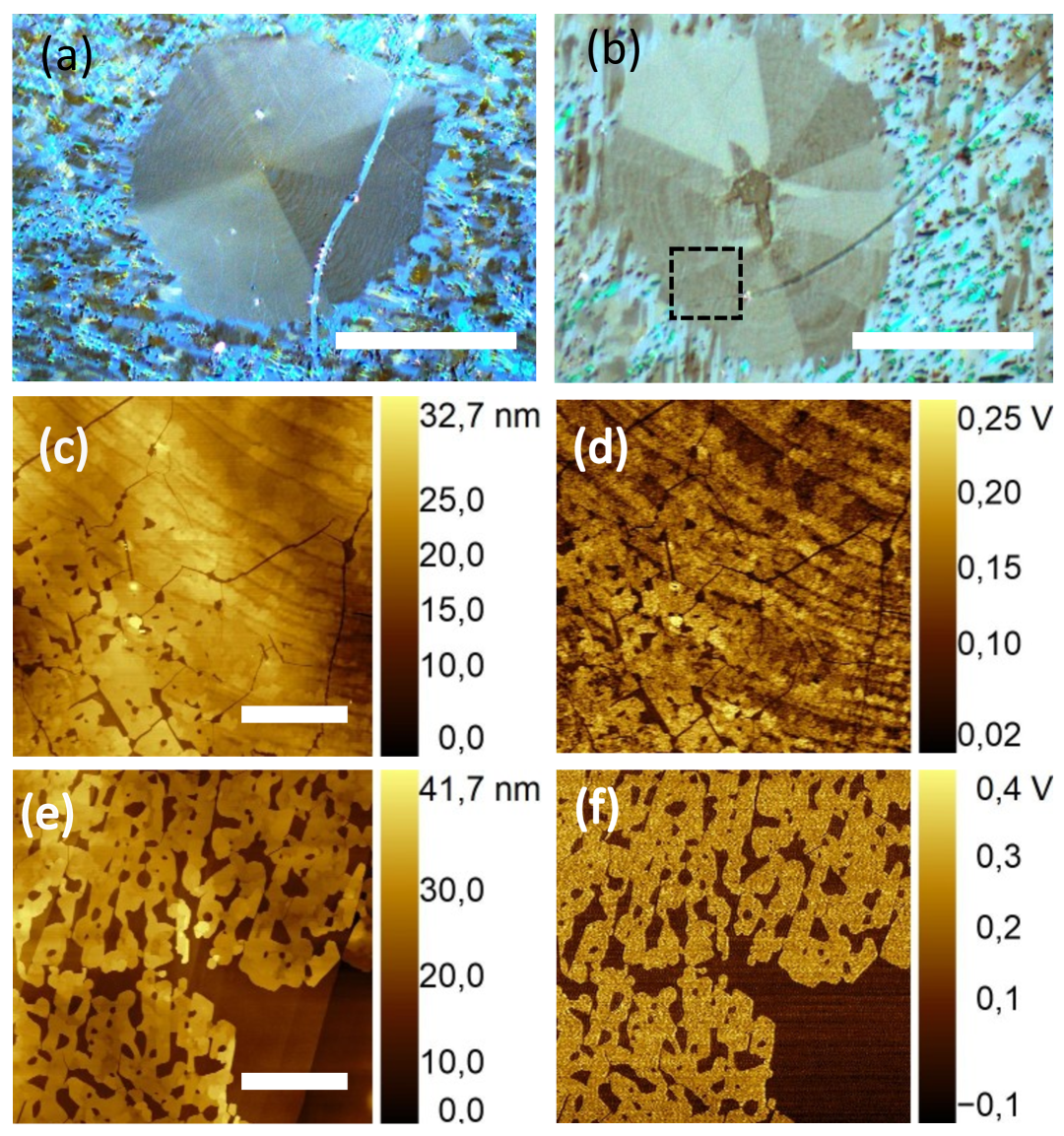
Figure 1a and 1b show POM images of two different rubrene orthorhombic platelets. The laterally extended thin crystals exhibit a smooth surface with a growth habit corroborating nucleation and growth from the center to the edges of the platelet. These platelets are surrounded by colonies of small crystals forming triclinic spherulites [19, 20] (not shown here).
The contrast observed in polarised optical microscopy (POM) is sometimes linked to line defects formed during sample preparation (Figure 1b), but it can also appear within a single domain in the absence of such defects (Figure 1a). It had been shown that these crystals grow with the c-axis of the orthorhombic unit cell perpendicular to the surface [20, 19]. This makes the ab-plane of the unit cell lying parallel to the crystal surface and transition dipole moment of S0-S1 normal to the surface [25].
Figure 1c and 1d are atomic AFM and KPFM maps of the dashed framed in Figure 1b. The line defects between domains are visible in the AFM topography. We measured the KPFM potential difference of rubrene crystals with varying thicknesses and morphologies, and found that the potential does not depend on thickness but varies with morphology, specifically with different molecule density as well as unit cell orientations [26].
The surface potential difference variation within the orthorhombic platelets is 100 to 150 meV. The lower local potentials could point to incomplete equilibration of last layer and lower molecule density which is corroborated by topography measurements (Figure 1c and 1d). Such KPFM contrast points towards a non-uniform molecular density throughout the crystal surface. The triclinic structures in the surrounding exhibit relatively homogeneous surface potential differences of 400 mV, compared to 200 mV on the HOPG substrate (Figure 1e and 1f).
In general, with increasing molecular density, the surface potential drops and the work function accordingly rises; the reason is that higher species density coming along with stronger vertical surface dipole. In ambient experiments, HOPG as well as thin films of aromatic molecules can adsorb airborne molecules with time, which will change the surface potential ([27, 28]). Additionally, ambient light can give rise to charge carrier generation, giving rise to surface potential modification.
Figure 2a and 2b show the PEEM images of the crystal shown in 1b, excited with different photon energies (6.2 eV and 3.1 eV respectively). Once the crystal is excited with 3.1 eV, the electron yields in the domain boundaries and line defects are higher than in regions with smooth and uniform morphologies, resulting in a pattern reminiscent to a spider web in Figure 2.b.
On the other hand, the 6.2 eV excitation results in a contrast in different domains and local regions of crystals. Unlike the 3.1 eV excitation, domain boundaries and line defects are not appearing bright with high electron yield.
We attributive the pronounced electron emission from domain boundaries (see 2b) to threshold emission from triplet exciton states accumulating at these locations, either via migration or by direct excitation. These states act like trap states which are populated by a first photon. Such processes are associated with a singlet fission upon absorption of the first photon [29, 30], followed by subsequent triplet exciton transfer.
Direct electron ejection from occupied states [31] as opposed to singlet fission, exciton migration and subsequent emission is much less likely for the 2PPE process compared to 1PPE. The latter results in a contrast governed by different local crystal orientations.
Since the c-axis of the orthorhombic unit cell is oriented along the dipole moment of HOMO-LUMO transition and in our crystals is almost perpendicular to the surface, a local rotation of this axis with respect to the surface normal yields a different angle between excitation polarisation and the dipole moment leading to different electron yields.
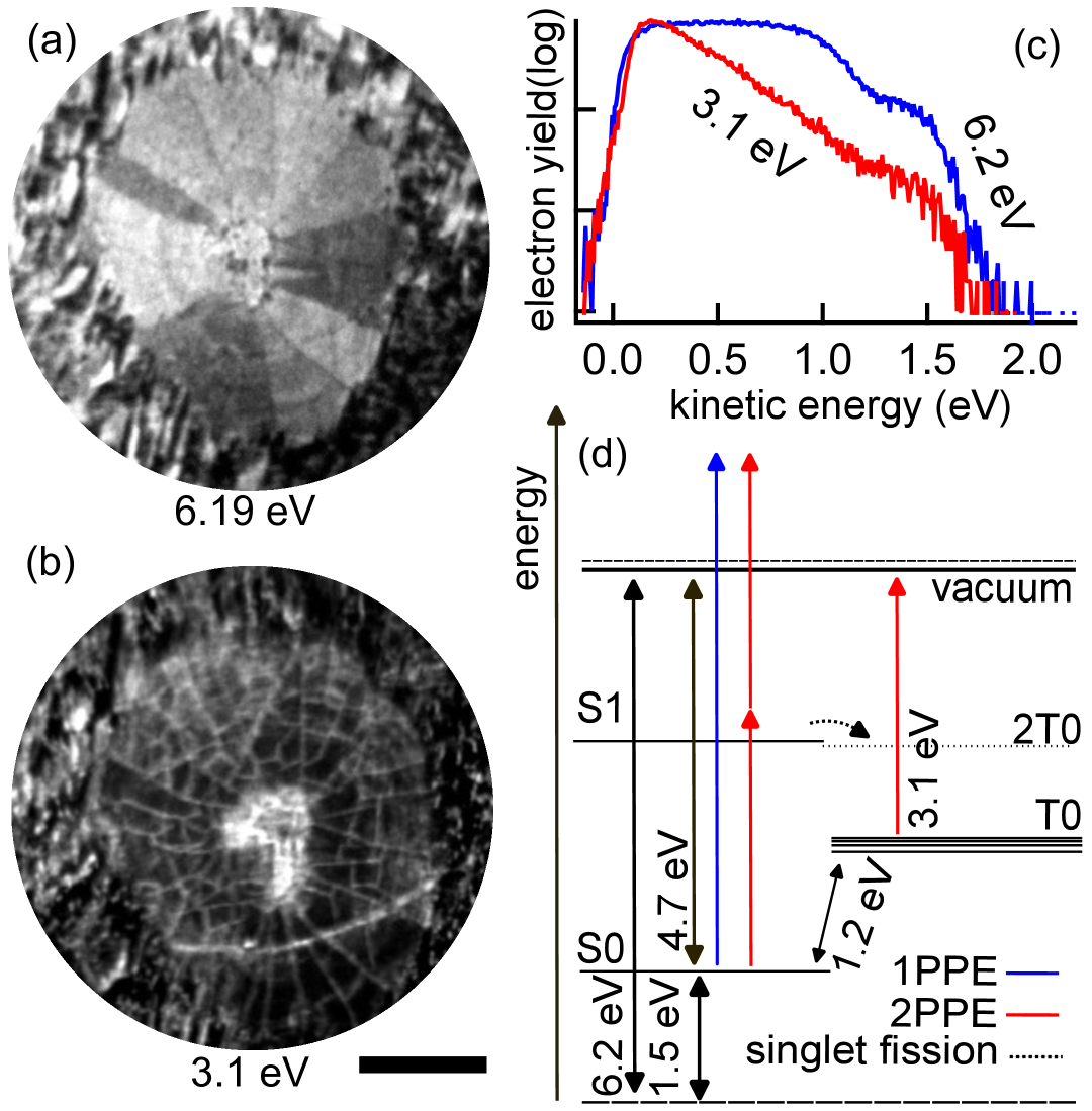
The electron spectra reflect the distinct nature of the involved photoemission processes. Figure 2c shows the electron spectra for two excitation sources with photon energies of 3.1 eV and 6.2 eV. The total width of the spectra is same for both 1PPE and 2PPE as expected, but similar kinetic energies point to different states, as pointed out in the following.
In a one-photon photoemission (1PPE) process, the electrons exhibiting the highest kinetic energies must originate from the highest occupied molecular orbital (HOMO), as higher-order excitations are absent. Therefore, the rightmost peak in the 1PPE spectrum can be attributed to the S0 state.
The total spectral width, which is approximately 2 eV thus corresponds to the energy difference between the state with the highest binding energy and the S0 state. The energy difference between the vacuum level and the state with the highest binding energy is equal to the photon energy used for excitation (6.2 eV). Based on this, the position of the vacuum level relative to the HOMO (S0) state is determined to be 4.2 eV above it, see Figure 2.
In the two-photon photoemission (2PPE) process, absorption of the first 3.1 eV photon initiates singlet fission, resulting in the formation of two triplet excitons, each with an energy approximately half that of the initial singlet (S0-S1) energy. Consequently, the energy difference between the vacuum level and the triplet state can be as large as 3 eV. Upon absorption of the second 3.1 eV photon in the 2PPE process, electrons emitted from the triplet state are expected to exhibit the lowest kinetic energies.
Accordingly, the leftmost peak in the 2PPE spectrum can be assigned to photoemission from the triplet state. The prominence of this peak points to a high density of trap states associated with domain boundaries and line defects within the crystal, as visible also in Figure 2b.
Consequently, the rightmost peak in the 2PPE spectra is originating from an true 2-photon absorption which results in an electron emission having kinetic energies at . The assigned photoemission processes are summarised in Figure 2.d. It is important to note that the energy resolution of our setup is approximately 50 meV. We estimate the work function of the orthorhombic rubrene crystal phase to be 4.2 eV. In addition, the time-to-energy conversion introduces an uncertainty of the order of 100 meV, which is comparable to the observed work function variations between local domains ( 200 meV).
Moreover, the spatial resolution of the of about 50 nm under the employed experimental conditions limits our ability to resolve photoemission signals from individual domains. As a result, the accuracy of energy assignments is further limited to 200 meV.
Nevertheless, PEEM utilising a two-photon photoemission (2PPE) process proves to be a powerful technique for assessing the quality of such crystals, particularly by revealing domain boundaries and defect-induced trap states that are not detectable with conventional polarised optical microscopy. As shown in Figures 1a and 1b, the line defects and domain boundaries are not visible; instead, the observed colour variations correspond to different crystal orientations. In contrast, Figures 2b and 3a—PEEM 2PPE images of the samples shown in Figures 1b and 1a, respectively—clearly reveal pronounced defect lines and domain boundaries, providing direct insight into the crystal quality.
As mentioned above, the emission from occupied states such as triplet or triplet-derived trap-like states implies a second-order process which is investigated in the following by analysing the photon order for different photon energies. Figure 3 shows the electron spectra of the crystal shown in 1a, resolved different crystal phases, excited with different photon energies. For electrons emitted with different kinetic energies, the photon order is also measured.
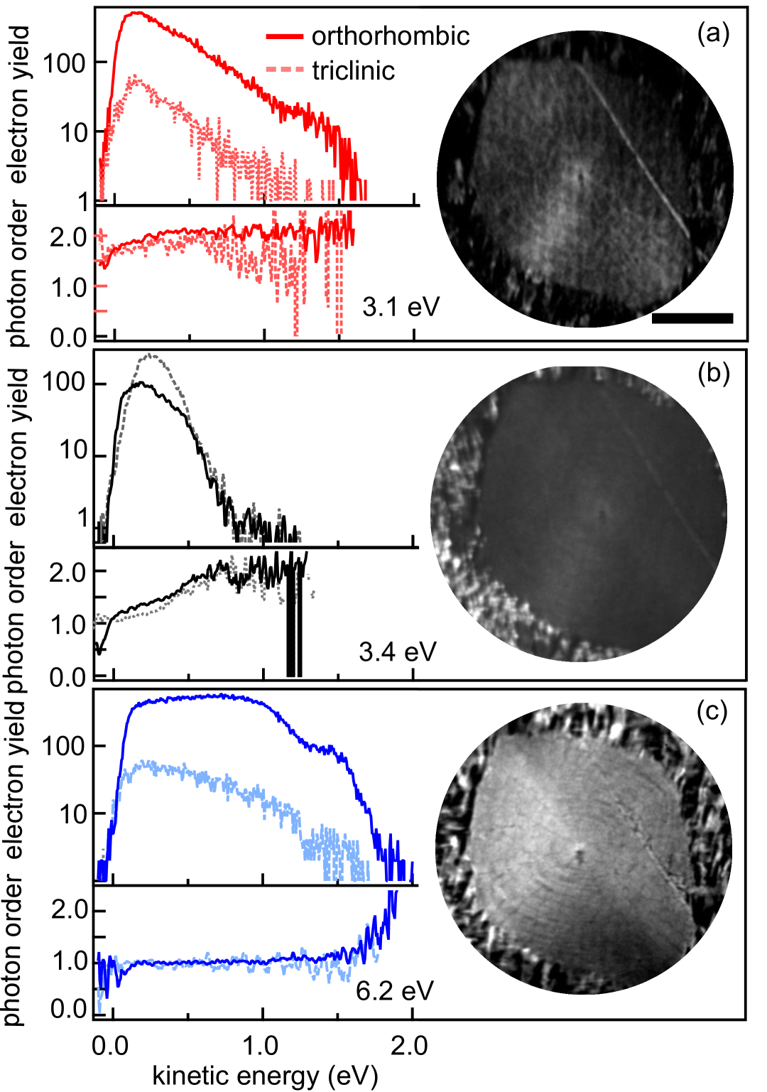
The photon order remains consistently equal to two across the entire spectral range when the sample is excited with 3.1 eV photons (Figure 3a), except for at lowest kinetic energies. The latter correspond to threshold emission, where the initial states are the above mentioned defect states at the domain boundaries. The reduction of the photon order points to partial saturation of these states and supports the energetic scheme in 2d.
For 6.2 eV excitation (Figure 3c), the photon order is constantly equal to 1. Only for electrons with highest kinetic energies, the photon order apparently approaches two. If such processes are involved, they indeed are expected at the highest kinetic energies. Alternatively, such an apparent second-order process could be due space-charge effects which tend to be most pronounced at the highest energies as well. Both possibilities can arise when the sample is excited with relatively intense light.
In an intermediate regime—where the excitation photon energies are above the 2PPE threshold but still below the work function of rubrene—a mixed photon order is observed. As shown in Figures 3b , the photon order evolves from one to two with increasing kinetic energy, when the excitation photon energy is 3.4 eV. For such intermediate photon energies, the extracted photon order deviates from integer values, falling between one and two suggests the involvement of multi-step excitonic dynamics rather than a pure multiphoton absorption process. At photon energies below the work function, an intermediate state may be populated, which can give rise to fractional photon orders if it is partially saturated.
An interesting observation is that the orthorhombic platelet is contributing to the photoemission only if there is an integer photon order and for a non-integer order, the crystal shows up dark and the signal is mostly coming from the needle-shape triclinic small crystals around the large domain (Figure 3.b).
Another contributing aspect for a non-integer photon order could be the non-uniformity of the work function across the orthorhombic crystal surface or among individual triclinic microcrystals. Such variations in local work function can lead to differences in the local photoemission order. Since the measured signal averages photoemission from the entire surface, encompassing multiple polymorphs, this results in an apparent non-integer photon order. This interpretation is in agreement with the observed increase in photon order with kinetic energy (see Figure 3b and 3c).
4 Conclusion
The photoemission signature and electron spectra of rubrene orthorhombic platelets prepared on HOPG were investigated. We showed that wavelength-dependent photoemission electron microscopy, combined with time-of-flight spectroscopy, provides a powerful approach to Figure out the internal electronic mechanisms and morphological quality of rubrene thin crystals. Our findings reveal that two-photon photoemission processes are highly sensitive to trap states and domain boundaries, while one-photon photoemission enables uniform surface imaging. The role of triplet excitons in two-photon emission processes was identified, offering new insight into charge transport dynamics in organic semiconductors. Additionally, the observation of a non-integer photoemission order for certain excitation photon energies, highlighting triclinic morphologies over orthorhombic, suggests that spectrally and spatially resolved photoemission could be applied for distinguishing crystalline phases. Surface potential maps of these crystals obtained by KPFM suggest that, such non-integer orders at certain photon energies arise due to spatial variations in the work function. These results establish a framework for quality assessment of organic electronic materials improving device fabrication and characterization.
Acknowledgment
Funding by the Deutsche Forschungsgemeinschaft (DFG, German Research Foundation) within project number INST 264/110-1 FUGG, SFB 1477 ”Light- Matter Interactions at Interfaces” and project number 441234705, SFB 1270 ”Electrically Active Implants” is acknowledged. We thank Sasankan Vinod Kumar and Gyanee Sita Babooram for their help with KPFM measurements.
References
- [1] Keke K. Zhang, Kejie Tan, Changji Zou, Magnus Wikberg, Laurie E. McNeil, Subodh G. Mhaisalkar, and C. Kloc. Control of charge mobility in single-crystal rubrene through surface chemistry. Organic Electronics, 11(12):1928–1934, December 2010.
- [2] Jun Nitta, Kazumoto Miwa, Naoki Komiya, Emilia Annese, Jun Fujii, Shimpei Ono, and Kazuyuki Sakamoto. The actual electronic band structure of a rubrene single crystal. Scientific Reports, 9(1), July 2019.
- [3] P. Baronas, G. Kreiza, L. Naimovičius, E. Radiunas, K. Kazlauskas, E. Orentas, and S. Juršėnas. Sweet spot of intermolecular coupling in crystalline rubrene: Intermolecular separation to minimize singlet fission and retain triplet–triplet annihilation. The Journal of Physical Chemistry C, 126(36):15327–15335, August 2022.
- [4] J.W. Bai, P. Chen, Y.L. Lei, Y. Zhang, Q.M. Zhang, Z.H. Xiong, and F. Li. Studying singlet fission and triplet fusion by magneto-electroluminescence method in singlet–triplet energy-resonant organic light-emitting diodes. Organic Electronics, 15(1):169–174, January 2014.
- [5] Drew M. Finton, Eric A. Wolf, Vincent S. Zoutenbier, Kebra A. Ward, and Ivan Biaggio. Routes to singlet exciton fission in rubrene crystals and amorphous films. AIP Advances, 9(9), September 2019.
- [6] ZhiYe Zhu, Hang Zang, Yi Zhao, and WanZhen Liang. Charge carrier mobilities and singlet fission dynamics in thienoquinoidal compounds. The Journal of Physical Chemistry C, 121(41):22587–22596, October 2017.
- [7] Aleksandr Ryasnyanskiy and Ivan Biaggio. Triplet exciton dynamics in rubrene single crystals. Physical Review B, 84(19), November 2011.
- [8] Jing Li, Zhonghai Chen, Qiaoming Zhang, Zuhong Xiong, and Yong Zhang. Temperature-dependent singlet exciton fission observed in amorphous rubrene films. Organic Electronics, 26:213–217, November 2015.
- [9] Geoffrey B. Piland, Jonathan J. Burdett, Dharmalingam Kurunthu, and Christopher J. Bardeen. Magnetic field effects on singlet fission and fluorescence decay dynamics in amorphous rubrene. The Journal of Physical Chemistry C, 117(3):1224–1236, January 2013.
- [10] Se-W. Park, Jung Min Hwang, Jeong-M. Choi, D. K. Hwang, M. S. Oh, Jae Hoon Kim, and Seongil Im. Rubrene thin-film transistors with crystalline and amorphous channels. Applied Physics Letters, 90(15), April 2007.
- [11] Yusuke Wakikawa and Tadaaki Ikoma. Triplet pair dynamics of singlet fission in orthorhombic polycrystalline powder of rubrene as revealed by magnetoluminescence. The Journal of Chemical Physics, 162(12), March 2025.
- [12] Ilana Breen, Roel Tempelaar, Laurie A. Bizimana, Benedikt Kloss, David R. Reichman, and Daniel B. Turner. Triplet separation drives singlet fission after femtosecond correlated triplet pair production in rubrene. Journal of the American Chemical Society, 139(34):11745–11751, August 2017.
- [13] Tanner S. Volek, Zachary T. Armstrong, Jakub K. Sowa, Kelly S. Wilson, Miriam Bohlmann Kunz, Kajari Bera, MaKenna Koble, Renee R. Frontiera, Peter J. Rossky, Martin T. Zanni, and Sean T. Roberts. Structural disorder at the edges of rubrene crystals enhances singlet fission. The Journal of Physical Chemistry Letters, 14(50):11497–11505, December 2023.
- [14] Hyun Ho Choi, Hee Taek Yi, Junto Tsurumi, Jae Joon Kim, Alejandro L. Briseno, Shun Watanabe, Jun Takeya, Kilwon Cho, and Vitaly Podzorov. A large anisotropic enhancement of the charge carrier mobility of flexible organic transistors with strain: A hall effect and raman study. Advanced Science, 7(1), November 2019.
- [15] Venkatesha R. Hathwar, Mattia Sist, Mads R. V. Jørgensen, Aref H. Mamakhel, Xiaoping Wang, Christina M. Hoffmann, Kunihisa Sugimoto, Jacob Overgaard, and Bo Brummerstedt Iversen. Quantitative analysis of intermolecular interactions in orthorhombic rubrene. IUCrJ, 2(5):563–574, August 2015.
- [16] Arie van der Lee, Maurizio Polentarutti, Gilles H. Roche, Olivier J. Dautel, Guillaume Wantz, Frédéric Castet, and Luca Muccioli. Temperature-dependent structural phase transition in rubrene single crystals: The missing piece from the charge mobility puzzle? The Journal of Physical Chemistry Letters, 13(1):406–411, January 2022.
- [17] Hyeok Moo Lee, Hanul Moon, Hyo-Sik Kim, Yong Nam Kim, Sung-Min Choi, Seunghyup Yoo, and Sung Oh Cho. Abrupt heating-induced high-quality crystalline rubrene thin films for organic thin-film transistors. Organic Electronics, 12(8):1446–1453, August 2011.
- [18] Alexandre L. Foggiatto, Yasuo Takeichi, Kanta Ono, Hiroki Suga, Yoshio Takahashi, Michael A. Fusella, Jordan T. Dull, Barry P. Rand, Kentaro Kutsukake, and Takeaki Sakurai. Study of local structure at crystalline rubrene grain boundaries via scanning transmission x-ray microscopy. Organic Electronics, 74:315–320, November 2019.
- [19] Moha Naeimi, Katharina Engster, Ingo Barke, and Sylvia Speller. Morphology and structural properties of thin rubrene crystallites grown on graphite. Physica Scripta, 100(1):015406, December 2024.
- [20] Julie Euvrard, Oki Gunawan, Antoine Kahn, and Barry P. Rand. From amorphous to polycrystalline rubrene: Charge transport in organic semiconductors paralleled with silicon. Advanced Functional Materials, 32(49), October 2022.
- [21] Jenna A. Tan, Jordan T. Dull, Steven E. Zeltmann, Jakhangirkhodja A. Tulyagankhodjaev, Holly M. Johnson, Alex Liebman‐Peláez, Brendan D. Folie, Sven A. Dönges, Omar Khatib, Jonathan G. Raybin, Trevor D. Roberts, Leo M. Hamerlynck, Christian P. N. Tanner, Jina Lee, Colin Ophus, Karen C. Bustillo, Markus B. Raschke, Hendrik Ohldag, Andrew M. Minor, Barry P. Rand, and Naomi S. Ginsberg. Multimodal characterization of crystal structure and formation in rubrene thin films reveals erasure of orientational discontinuities. Advanced Functional Materials, 33(13), January 2023.
- [22] Thomas R. Fielitz and Russell J. Holmes. Crystal morphology and growth in annealed rubrene thin films. Crystal Growth and Design, 16(8):4720–4726, July 2016.
- [23] Michael A. Fusella, Frank Schreiber, Kevin Abbasi, Jae Joon Kim, Alejandro L. Briseno, and Barry P. Rand. Homoepitaxy of crystalline rubrene thin films. Nano Letters, 17(5):3040–3046, April 2017.
- [24] David Nečas and Petr Klapetek. Gwyddion: an open-source software for spm data analysis. Open Physics, 10(1):181–188, December 2011.
- [25] Pavel Irkhin, Aleksandr Ryasnyanskiy, Marlus Koehler, and Ivan Biaggio. Absorption and photoluminescence spectroscopy of rubrene single crystals. Physical Review B, 86(8), August 2012.
- [26] Yanfei Wu, Annabel R. Chew, Geoffrey A. Rojas, Gjergji Sini, Greg Haugstad, Alex Belianinov, Sergei V. Kalinin, Hong Li, Chad Risko, Jean-Luc Brédas, Alberto Salleo, and C. Daniel Frisbie. Strain effects on the work function of an organic semiconductor. Nature Communications, 7(1), February 2016.
- [27] David Martinez-Martin, Raphael Longuinhos, Jesus G. Izquierdo, Antonela Marele, Simone S. Alexandre, Miriam Jaafar, Jose M. Gómez-Rodríguez, Luis Bañares, Jose M. Soler, and Julio Gomez-Herrero. Atmospheric contaminants on graphitic surfaces. Carbon, 61:33–39, September 2013.
- [28] Takeshi Terada, Jayesh A. Kulkarni, Ariel Huynh, Sam Chen, Roy van der Meel, Yuen Yi C. Tam, and Pieter R. Cullis. Characterization of lipid nanoparticles containing ionizable cationic lipids using design-of-experiments approach. Langmuir, 37(3):1120–1128, January 2021.
- [29] R.T. Williams and K.S. Song. The self-trapped exciton. Journal of Physics and Chemistry of Solids, 51(7):679–716, January 1990.
- [30] Gleb M. Akselrod, Parag B. Deotare, Nicholas J. Thompson, Jiye Lee, William A. Tisdale, Marc A. Baldo, Vinod M. Menon, and Vladimir Bulović. Visualization of exciton transport in ordered and disordered molecular solids. Nature Communications, 5(1), April 2014.
- [31] D. Okaue, R. Hayashi, K. Wakayama, N. Ito, T. Munakata, and T. Yamada. Lateral distribution of optical excitation at boundaries around rubrene islands visualized by microspot two-photon photoemission spectroscopy. Surface Science, 709:121847, July 2021.