Modeling PFAS in Semiconductor Manufacturing to Quantify Trade-offs
in Energy Efficiency and Environmental Impact of Computing Systems
Abstract—The electronics and semiconductor industry is a prominent consumer of per- and poly-fluoroalkyl substances (PFAS), also known as forever chemicals. PFAS are persistent in the environment and can bioaccumulate to ecological and human toxic levels. Computer designers have an opportunity to reduce the use of PFAS in semiconductors and electronics manufacturing, including integrated circuits (IC), batteries, displays, etc., which currently account for a staggering 10% of the total PFAS fluoropolymers usage in Europe alone. In this paper, we present a framework where we (1) quantify the environmental impact of PFAS in computing systems manufacturing with granular consideration of the metal layer stack and patterning complexities in IC manufacturing at the design phase, (2) identify contending trends between embodied carbon (carbon footprint due to hardware manufacturing) versus PFAS. For example, manufacturing an IC at a 7 nm technology node using EUV lithography uses 18% less PFAS-containing layers, compared to manufacturing the same IC at a 7 nm technology node using DUV immersion lithography (instead of EUV) unlike embodied carbon trends, and (3) conduct case studies to illustrate how to optimize and trade-off designs with lower PFAS, while meeting power-performance-area constraints. We show that optimizing designs to use less back-end-of-line (BEOL) metal stack layers can save 1.7 PFAS-containing layers in systolic arrays.
I Introduction
The environmental impacts of computing systems go beyond their carbon footprint and water consumption. The chemicals and materials used in the semiconductor and electronics manufacturing processes have environmental and human health impacts that require our immediate attention as computer designers and engineers. A class known as per- and poly-fluoroalkyl substances (PFAS)—also referred to as forever chemicals—constitutes more than 16,000 chemicals used in manufacturing across global industries [1]. PFAS are a physiochemically diverse class of synthetic chemicals, containing one or more fully fluorinated methyl (three carbon-fluorine bonds) or ethylene (two carbon-fluorine bonds) carbon atoms [2]. Due to their bioaccumulation, human toxicity, and environmental impact, PFAS have been under extensive public, scientific and regulatory action globally [3, 4, 5]. Across the electronics and semiconductor industry, PFAS are used in a wide variety of capacities including manufacturing computing ICs, displays, batteries, cooling liquids for thermal management in datacenters, and more [1, 6, 7]. With the rising proliferation of electronics and computing chips, PFAS use in electronics are expected to grow 10% annually, primarily driven by semiconductor manufacturing and production [5].
| Part | PFAS Type | Use | Function | Alternatives |
| photopolymer | photolithography | photoresist | no alternative yet (research stage) [9, 10] | |
| photopolymer | photolithography | photoacid generator | no alternative yet (research stage) [9, 10] | |
| short fluoropolymers | anti-reflective coating | low refractive index | available but not demonstrated in DUV [9] | |
| Integrated Circuits | short-chain PFAS | developers | remove unwanted resist pattern | no alternative yet (research stage) [9] |
| PFAS additives | rinsing solutions | low-surface tension | no alternative yet (research stage) [11] | |
| fluorocarbon gases | dry etching | precision in etching | no alternative yet (research stage) [1] | |
| fluorosurfactants [12] | wet etching | improve coating quality | available (testing & trials stage) [13, 11] | |
| fluoropolymers | spin-on dielectrics | leakage blocker | available [14] | |
| Datacenters | fluorocarbons [15] | cooling liquids | refrigerants; thermal management | available (research stage) [16] |
| PCBs | fluoropolymer [17] | laminate material | flame retardant; dielectric | redesign equipment & product dimensions [18] |
| fluoropolymer | protective coating | temperature stable; dust repellent | multiple available [19] | |
| Capacitors | fluoropolymers | dielectric films | dielectric strength | multiple available [16] |
| Acoustic equipment | fluoropolymers | piezoelectric materials | mold into thin, flexible sheets | available depending on product function |
| fluoropolymers | vent membranes | hydrophobic | no alternative yet (research stage) | |
| Displays | fluorinated compounds | LCD | dipole moment | available e.g., LED or plasma screens [16] |
| Wiring & cables | fluoropolymers | insulating layer | corrosion, thermal, cracking resistant | available depending on needed function |
| Lithium-ion batteries | fluoropolymers | binder | electrochemical stability | no alternative yet (research stage) |
| PFAS salts & additives [20] | electrolyte | increased performance & durability | available |
As more fabrication facilities are built globally, the increasing use of PFAS during manufacturing as well as PFAS contaminants, whether through wastewater, emissions, or increasing e-waste [21], are pressing environmental issues for the semiconductor and computing industry at large. In this paper, we take a data-driven approach to studying PFAS in ICs manufacturing. We model PFAS use in different lithography manufacturing steps and identify design optimization trade-offs between PFAS, embodied carbon, power and performance. To our knowledge, this is the first work to enable researchers and designers to model and quantify PFAS from hardware manufacturing while proposing design strategies to minimize PFAS at the design phase. Our key contributions:
-
①
We propose an analytical modeling framework to quantify the amount of PFAS used in logic semiconductor manufacturing (section III). Our framework leverages detailed fabrication facility characterization and existing literature on semiconductor photolithography and processing complexity, to enable designers to estimate the PFAS consumption of their designs during manufacturing at the design phase.
-
②
To enable more holistic sustainable computing systems design, we integrate an architectural carbon modeling tool [22] in our framework to quantify and trade-off PFAS with carbon emissions due to hardware manufacturing (section IV and section V-A).
-
③
We conduct PFAS-aware design case studies (section V) and propose design knobs for designers to make less PFAS-containing designs. We demonstrate designing hardware systems with less number of back-end-of-line (BEOL) metal layers can lead to 1.7 less PFAS in manufacturing (section V-B).
II Background
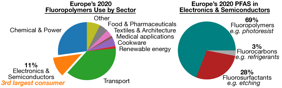
In Europe alone in 2020, European Chemicals Agency (ECHA) estimates the amount of PFAS used in electronics and semiconductor manufacturing to reach 4.21 kilotonnes [1]. Figure 1 (right) shows that approximately 69% of those PFAS come from fluoropolymers, 28% are fluorosurfactants used for surface wetting and modification, and 3% are fluorocarbons which are small molecule liquids and gases, some of which are greenhouse gases used in thermal management coolants. Another analysis shows that the electronics and semiconductors industry is the third largest consumer of fluoropolymers after the transportation and the chemical and power sectors as shown in Figure 1 (left), amounting to 11% of total fluoropolymers sold in the EU in 2020 [8, 23].
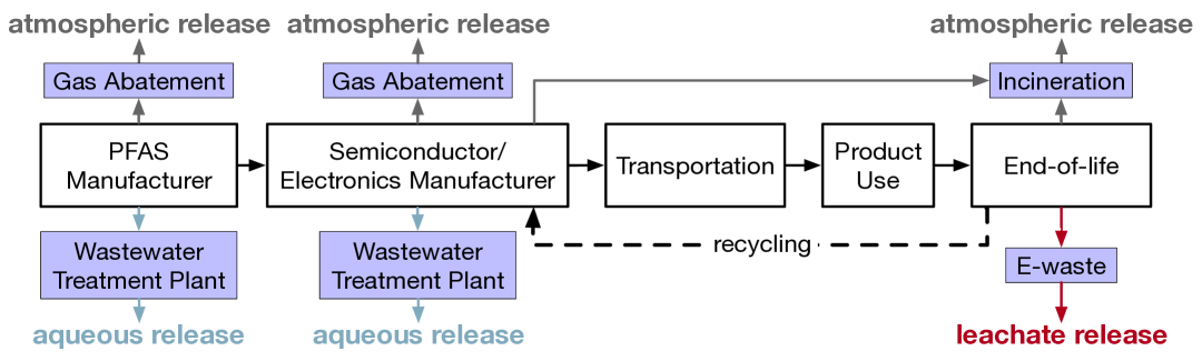
Many PFAS are environmentally persistent and bioaccumulative, and have been found in water, soil, and air (including the arctic) [24, 4]. While the toxicological data of most PFAS are currently largely undetermined [25, 26], the potential health consequences and bioaccumulation of forever chemicals stipulate the alarming need for minimizing the use of PFAS whenever possible. Only few technology companies, such as Apple [6], have announced the phasing out of PFAS in their products. While PFAS are mostly safe during product use, many safety concerns arise throughout the manufacturing supply chain and disposal of computing systems. Throughout the computing system’s lifecycle, there are three possible flows for PFAS to be released into the environment, namely atmospheric release through air, aqueous release through water, and leachate release through soil. Figure 2 illustrates these three potential PFAS contamination streams for semiconductors.
PFAS remediation methods, i.e. removing PFAS contaminants from water sources and soil, are important solutions towards limiting human exposure to already existing PFAS. However, they are insufficient to overcome PFAS pollution across industries [27, 28]. Recent studies show that wastewater treatment plants do not fully remove or eradicate PFAS from semiconductor fabrication facilities’ wastewater. Furthermore, certain PFAS are systematically resistant to current wastewater treatments [29, 30]. This highlights the importance of reducing PFAS-containing chemicals in manufacturing, and even prior at the design phase. Therefore, there is a critical need to find effective PFAS-free alternatives and minimize PFAS when their use is necessary in computing (e.g. photolithography). In Table I, we show different types of PFAS used in a variety of electronics and semiconductor manufacturing processes, as well as the current availability of viable PFAS-free alternatives, or lack thereof.
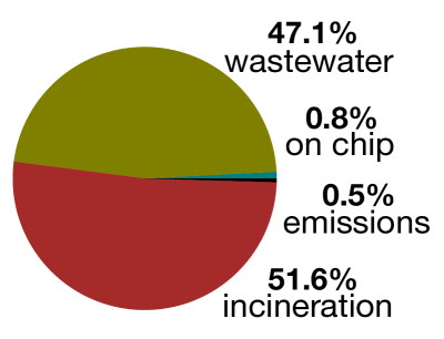
The primary use of PFAS in semiconductor manufacturing is in photolithography, where only 0.8% of PFAS used remain on chip [31], and the majority are either disposed of in wastewater or incinerated (Figure 3). Building environmentally sustainable computing systems, including low PFAS consumption, requires collaborations across the computing stack, from design to manufacturing to disposal, and collective collaboration among academia and industry. Researchers and designers across the computing stack have an opportunity to identify trade-offs and incorporate optimizations for lower environmental impacts of PFAS at the design phase, especially due to the current lack of PFAS-free alternatives in photolithography and ICs manufacturing. PFAS are primarily used in:
-
1.
Photoresists. These are photopolymers used to pattern micro and nano structures on a substrate by changing its solubility upon exposure to short wavelength radiation, such as extreme ultraviolet (EUV) or deep ultraviolet (DUV). This process requires yield above 99% given the many process steps needed to manufacture advanced semiconductor chips [9].
-
2.
Antireflective coatings (ARCs). Used for their low refractive index, to prevent light interference reflected from substrate, and as a barrier layer. These include top and bottom antireflective coats (TARCs and BARCs, respectively).
-
3.
Other coatings. Such as topcoats are used to prevent leaching of photoactive components and protect photoresist from immersion water used in 193 nm immersion DUV [9]. Furthermore, dielectric spin-on coatings improve coating uniformity in photoresists and ARCs and prevent defects.
We identify lithography steps which include PFAS chemicals and refer to them as PFAS-containing layers in this work. section III details the design and implementation of the proposed PFAS modeling tool for semiconductor manufacturing.
III Framework for PFAS-Aware Systems Design
Computer designers have a key opportunity to minimize PFAS at the design phase. In this section, we detail how we quantify and model the amount of PFAS used in semiconductor manufacturing per metal layer of IC design based on fabrication specifications (section III-A). We detail the inputs and outputs of our framework (section III-B), and discuss limitations and future steps for researchers and designers to better account for PFAS in computing systems (section III-C).
III-A PFAS and Semiconductor Manufacturing Analytical Model
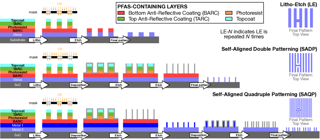
The amount of PFAS used in semiconductor manufacturing is highly dependent on complexity of patterning and metal layer stack. In Figure 4, we illustrate the process complexities and PFAS-containing layers of the most commonly used lithography options in semiconductor manufacturing, including Litho-Etch (LE), Self-Aligned Double Patterning (SADP), and Self-Aligned Quadruple Patterning (SAQP). Depending on the process flow and chemicals used, the amount of PFAS and combined use of antireflective coats, spin-on coats and topcoats with a specific photoresist vary. For example, one process flow may include BARC and photoresist only [32]. Our model offers the flexibility for designers and engineers to update and customize the patterning complexity and process flow of a given process technology node, allowing for the integration of user-defined fabrication specifications.
| Process | # Steps [33] | # Masks | ||||||
|---|---|---|---|---|---|---|---|---|
| DryEtch | Litho. | Metal. | Metr. | WetEtch | Dep. | |||
| ArF LE | 1 | 3 | 1 | 2 | 3 | 0 | 1 | |
|
DUV |
ArFi LE | 1 | 3 | 1 | 3 | 3 | 0 | 1 |
| ArFi LE-2 | 3 | 6 | 1 | 7 | 3 | 1 | 2 | |
| ArFi LE-3 | 4 | 9 | 1 | 10 | 3 | 1 | 3 | |
| ArFi LE-4 | 5 | 12 | 1 | 13 | 3 | 1 | 4 | |
| ArFi SADP | 3 | 3 | 1 | 5 | 5 | 3 | 1 | |
| ArFi SAQP | 3 | 2 | 1 | 7 | 7 | 10 | 1 | |
|
EUV |
LE | 1 | 3 | 1 | 3 | 3 | 0 | 1 |
| SA LE-2 | 5 | 6 | 1 | 8 | 7 | 3 | 2 | |
We base our current PFAS model on the metal stacks presented in [33, 34], and approximate the amount of PFAS-containing layers based on the lithography steps which typically use PFAS-containing photoresist, ARCs, topcoats and other coatings. In semiconductor manufacturing, masks are used to lithographically pattern features on silicon wafers. Therefore, we use the number of lithography masks as a proxy to estimate the amount of PFAS used in manufacturing (Table II). The analytical PFAS modeling equations are:
| (1) | ||||
| (2) |
We quantify the amount of PFAS in semiconductor manufacturing for 130 nm to 3 nm process technology nodes. In Figure 5, we show the PFAS-containing lithography layers in chip manufacturing across front-end-of-line (FEOL), middle-of-line (MOL) and back-end-of-line (BEOL). The amount of PFAS-containing layers increase with increasing number of lithography steps during IC fabrication. Using direct EUV results in less PFAS-containing layers compared to DUV, which correspond to lower number of masks and process steps (refer Figure 5). However, as feature sizes get smaller, the number of masks and lithography steps increase due to the rising complexity of more advanced technology nodes.

| Parameter | Description | Range |
|---|---|---|
| M | Number of BEOL metal layers | From HW design (M1 – M20) |
| p | Process technology node | 180 nm – 3 nm |
| c | Patterning complexity | From fab (DUV, EUV, SADP, etc.) |
| f | Process flow | From fab |
| Y | Fab yield | From fab (0 – 1) |
| A | Die area | From HW design (cm2) |
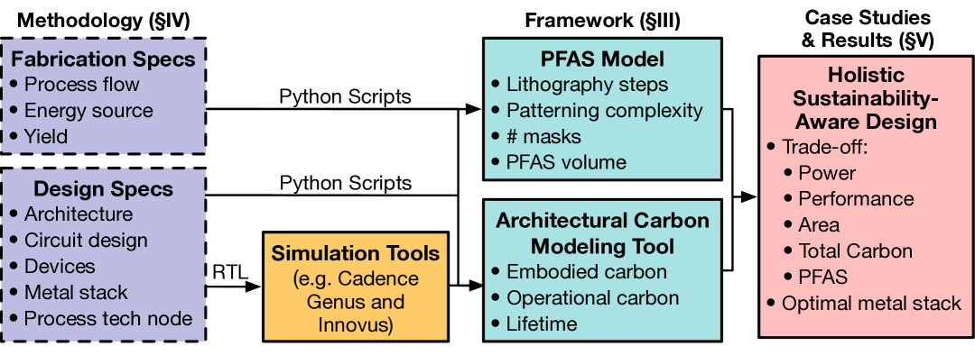
III-B PFAS Framework
We detail our proposed framework for PFAS and carbon aware design in Figure 6. Our framework takes input parameters across multiple layers of the computing stack, from fabrication facility specifications, such as yield and process flow, to metal stack specifications and architecture of the design as well as power, performance and die area. Table III defines each of the input parameters in our framework. The inputs are fed into our PFAS model and an architectural carbon modeling tool ACT [22]. This enables holistic sustainability-aware design by trading-off power, performance, area, PFAS and carbon emissions of different computing systems (refer section V). In addition, our model can be extended to include other process flows, metal stacks, and PDKs to quantify and estimate PFAS use for a variety of manufacturing processes at the design phase. For example, we show the estimated number of PFAS-containing layers based on metal line processes of ASAP7 PDK in Table IV (table does not include doping masks in FEOL for brevity).
III-C Limitations
While our PFAS model is the first to enable designers and researchers to quantify PFAS in semiconductor manufacturing at the IC design phase, there are some limitations due to lack of manufacturing data and PFAS quantification transparency across the supply chain.
First, the environmental impact of PFAS in computing is complex and understudied. Quantifying PFAS is a two-step process. First: environmental scientists need to detect PFAS, and second: they need to be able to measure PFAS. However, unlike carbon footprint, which can be measured and converted in units of carbon dioxide equivalent (CO), measuring PFAS is more challenging. With the variation in PFAS chain lengths (i.e. number of perfluorinated carbon), PFAS concentration (units of parts-per-trillion or g/L) while used in some studies [35], may not be a sufficient indicator alone for PFAS environmental impact. Alternatively, referring to amount of PFAS in fluorine basis, such as chain length [36, 31] or molarity equivalence will enable more accurate comparisons between different PFAS. For example, a PFAS substance with 1 perfluorinated carbon can be referred to as C1, versus another with 8 perfluorinated carbons is referred to as C8.
| Layers | M | Metal | Via [37] | # Litho steps | E | # PFAS | |
|---|---|---|---|---|---|---|---|
|
FEOL |
Fin | 27 | SAQP | - | 2 | 1 | 1 |
| Active | 108 | EUV LE | - | 3 | 10 | 1 | |
| Gate | 54 | SADP | - | 3 | 1 | 1 | |
| SDT | 54 | EUV LE | - | 3 | 10 | 1 | |
|
MOL |
LISD | 54 | EUV LE | - | 3 | 10 | 1 |
| LIG | 54 | EUV LE | - | 3 | 10 | 1 | |
| VIA0 | 25 | - | EUV LE | 3 | 10 | 1 | |
|
BEOL |
M1 | 36 | EUV LE | EUV LE | 6 | 20 | 2 |
| M2 | 36 | EUV LE | EUV LE | 6 | 20 | 2 | |
| M3 | 36 | EUV LE | EUV LE | 6 | 20 | 2 | |
| M4 | 48 | SADP | ArFi LE-2 | 9 | 3 | 3 | |
| M5 | 48 | SADP | ArFi LE-2 | 9 | 3 | 3 | |
| M6 | 64 | SADP | ArFi LE-2 | 9 | 3 | 3 | |
| M7 | 64 | SADP | ArFi LE-2 | 9 | 3 | 3 | |
| M8 | 80 | ArFi LE | ArFi LE | 6 | 2 | 2 | |
| M9 | 80 | ArFi LE | ArFi LE | 6 | 2 | 2 | |
Second, IC foundries and chemical companies maintain strict secrecy regarding their process flows, chemical usage, and the chemical composition of PFAS-containing chemicals like photoresists and ARCs. Even if fabrication data are available, there is a wide variation in process steps and recipes across foundries, including for the same process technology node. To overcome these challenges, we quantify PFAS through the number of PFAS-containing layers in semiconductor manufacturing. Given the growing semiconductor industry, we emphasize the need for public and transparent reporting of the environmental impacts of computing across the supply chain to enable research and industry efforts towards building more sustainable computing systems.
IV Evaluation Methodology
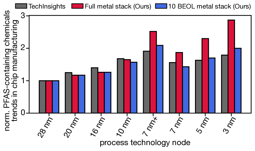
PFAS Quantification Validation. We validate our modeling methodology against the volume of PFAS-containing chemicals per technology node modeled by TechInsights [38]. In Figure 7, we show the PFAS trends in manufacturing across process technology node normalized to 28 nm. Our model exhibits similar trends to the volume of PFAS-containing chemicals quantified by TechInsights. However, TechInsights provide only coarse-grained data of PFAS and only post 28 nm technology. Our PFAS model is a parametric and predictive model that builds on foundries process flows, process complexities, and metal stacks to provide sufficient flexibility and versatility to quantify and reduce PFAS use in chip manufacturing at the design phase.
Carbon Footprint. To quantify the carbon footprint of ICs we integrate, ACT [22], an architectural carbon modeling tool into our framework for holistic sustainable computing design.
V Case Studies for PFAS-Aware Computing Design
In this section, we first show there is contention between embodied carbon versus PFAS as advanced technology nodes adopt EUV lithography. Second, we quantify the PPA, embodied carbon, and PFAS trade-offs of manufacturing a systolic array [40] with different number of BEOL (i.e. routing) metal layers. Third, we illustrate the overall PFAS benefit for optimizing a system on chip (SoC) with less BEOL metal layers versus area trade-offs.
V-A PFAS-Power-Performance-Carbon Design Trade-offs
To truly design more sustainable computing systems, designers need to account for environmental impacts, such as carbon footprint and PFAS, along with the conventional metrics of performance and power. In Figure 8, we show the performance, power, PFAS, and embodied carbon trends for 1 cm2 chips from 16 nm to 3 nm (x-axis) process technology nodes based on TSMC’s scaling [41, 42]. While performance and power improve with scaling, the environmental impacts of manufacturing, including embodied carbon and PFAS, do not necessarily improve with more advanced technology nodes. For embodied carbon, the general trend is increasing with more advanced technology nodes, due to increasing energy consumption with patterning complexity [33]. For PFAS-containing layers, the 7 nm (EUV) and 5 nm process technology nodes can incur lower environmental impact than 7 nm (DUV) and even 10 nm, depending on the BEOL metal stack (refer Figure 7), design area savings, and yield.
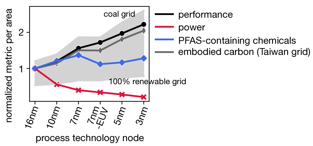
To illustrate, manufacturing a 7 nm process technology node design with EUV as described in [33, 41], is more environmentally sustainable than using DUV immersion multiple patterning [33] for the same metal layer stack, resulting in both lower embodied carbon and 18% less PFAS-containing layers (20% less volume of PFAS-containing chemicals [38]) during manufacturing. This is because direct EUV helps reduce the number of masks and manufacturing steps, including lithography, deposition and etching. One direct EUV mask can replace up to five immersion DUV masks, with better patterning yield and shorter fabrication time. EUV consumes on average 10 more power per tool than traditional DUV, but replaces multiple processing steps in fabrication [33].
V-B BEOL Metal Layers Reduction for PFAS Optimization
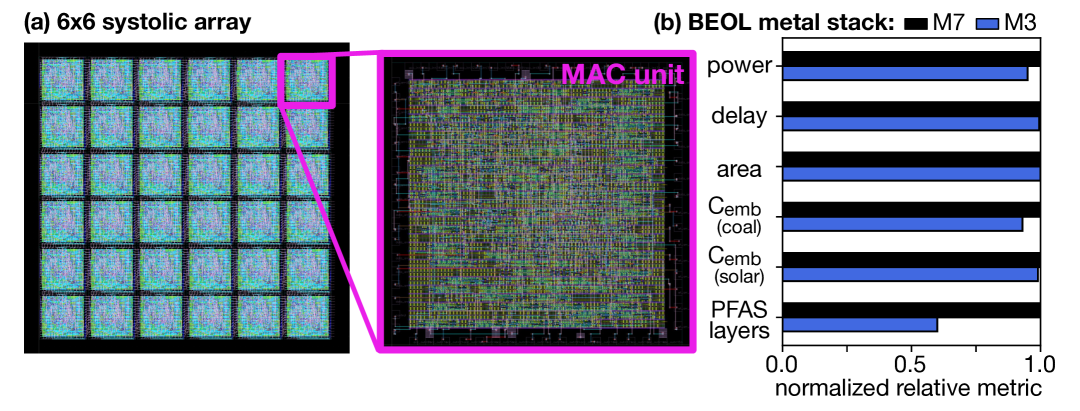
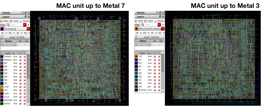
Given PFAS varies with number of metal layers, we quantify the trade-offs between embodied carbon, PFAS, and PPA, for example systolic arrays shown in Figure 9(a), routed to different BEOL metal layers. In Figure 9(b), we show that optimizing designs to use less BEOL metal layers can save up to 3 PFAS-containing layers across BEOL. Reducing the number of BEOL metal layers for a systolic array from Metal 7 (M7) to Metal 5 (M5) reduces the number of PFAS containing layers by 1.5, and further optimization to Metal 3 (M3) results in another 2 PFAS reduction benefit in BEOL with negligible PPA penalties due to systolic array’s regularity. For embodied carbon footprint, reducing BEOL layers is more impactful when fabrication facilities are powered by non-renewable energy sources (e.g. coal) rather than renewables (e.g. solar), due to electricity being the primary source of embodied carbon footprint. Therefore, the primary benefit of reducing BEOL metal layers is to reduce number of PFAS-containing layers in IC manufacturing. We show the place-and-route layouts of systolic array MAC units when unconstrained to M7 versus constrained down to M3 in Figure 10.
V-C Metal Layers vs. Area Trade-off for SoC PFAS optimization
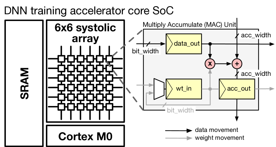
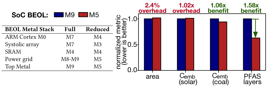
To illustrate the impact of optimizing BEOL metal layers to reduce PFAS on an SoC scale, we model a deep neural network (DNN) training accelerator [43], which includes an ARM Cortex-M0, a systolic array, and an on-chip SRAM, using the ASAP7 PDK metal stack (Figure 11). We do unconstrained place-and-route for the systolic array and Cortex-M0, which occupy up to M7, then optimize the BEOL metal stack routing down to M4. For the processor Cortex-M0, the area overhead increased by 1.47 to enable routing to M4. However, routing the Cortex-M0 down from M7 to M4 only results in 2.4% increase in the total SoC area. There is no area penalty for SRAM cells since they are typically routed to M4. In Figure 12, we detail the SoC’s BEOL metal stack when routed up to M9 (M8-M9 for power grid) and show a 1.58 PFAS reduction benefit by optimizing to M5.
Furthermore, we quantify the embodied carbon footprint of each SoC, based on the semiconductor fabrication facility’s carbon intensity and the BEOL metal stack. In both carbon intensity cases, reducing the number of BEOL metal stack, while accounting for the area overhead, has negligible effect on chip’s embodied carbon footprint. This is primarily due to the complexity of embodied carbon accounting which includes electricity consumption during fabrication (i.e. different tools and processes), materials procurement, and direct gas emissions. In contrast, the benefits of reducing number of PFAS containing layers are 10 more significant.
VI Opportunities & Call to Action
Optimizing the environmental impact of computing systems extends beyond carbon footprint to include materials and chemicals used in manufacturing such as PFAS. As regulatory PFAS guidance is evolving, it is critical for the semiconductor supply chain, including IC manufacturing, to minimize and eliminate PFAS use whenever possible. As designers, we have the opportunity to identify trade-offs and incorporate optimizations in our designs to consume less PFAS during manufacturing. In this section, we outline opportunities and future design strategies for reducing PFAS to design more environmentally sustainable computing systems.
First and foremost, more accurate and standardized PFAS quantification methods are needed as discussed in section III-C. Additionally, designers and archtiects have the opportunity to design and repurpose hardware for longer use to minimize e-waste. By extending hardware lifetime, designers can minimize the amount of e-waste sent to landfills and incineration sites, resulting in less PFAS polluting the atmosphere or leaching into the soil and aqueous streams.
Furthermore, there are opportunities to explore and advance the environmental sustainability of heterogeneous chiplet systems. State-of-the-art VLSI systems use multi-chip integration techniques including chiplets, i.e. assembling separately packaged die on a substrate known as interposer. Chiplets have the benefit of using small modular chips, which can help improve yield and also minimize the number of BEOL metal layers across the chip. For example, instead of routing the SoC to the maximum number of BEOL layers required (e.g. SoC to M7), each block can be manufactured up to the metal layer it requires (e.g. SRAM to M4), potentially reducing PFAS. However, chiplets also require packaging, which may introduce more PFAS and the power, performance, and carbon trade-offs versus monolithic SoCs are still unclear. This is an open area of research, which we hope framework lays the foundation for the computing community to explore.
VII Conclusion
The environmental impacts of computing systems, including carbon emissions and forever chemicals, are an escalating global concern. Semiconductor and electronics manufacturing rely heavily on the pervasive use of PFAS-containing materials, which pose uncertain bioaccumulation and human health risks. As reliance on technology grows, these hidden chemicals present urgent sustainability challenges. We propose a framework to enable designers and researchers to quantify PFAS and optimize computing systems for environmental sustainability—carbon footprint, PFAS, power, performance, and area—at the design phase. This work aims to lay the foundation for future research and optimization efforts to reduce PFAS in computing.
References
- [1] X. Lim, “Could the world go PFAS-free? Proposal to ban ‘forever chemicals’ fuels debate,” Nature, 2023.
- [2] O. F. E. COOPERATION et al., “Reconciling Terminology of the Universe of Per- and Polyfluoroalkyl Substances: Recommendations and Practical Guidance,” 2021. [Online]. Available: https://one.oecd.org/document/ENV/CBC/MONO(2021)25/En/pdf
- [3] 3M, “PFAS and Their Uses,” 2024. [Online]. Available: https://pfas.3m.com/pfas_uses
- [4] U. E. P. Agency, “Drinking Water Health Advisories for PFOA and PFOS. 2022 Interim Updated PFOA and PFOS Health Advisories,” 2022. [Online]. Available: https://www.epa.gov/sdwa/drinking-water-health-advisories-pfoa-and-pfos
- [5] E. C. Agency, “ANNEX XV RESTRICTION REPORT: PROPOSAL FOR A RESTRICTION,” 2023. [Online]. Available: https://echa.europa.eu/documents/10162/f605d4b5-7c17-7414-8823-b49b9fd43aea
- [6] Apple, “Apple’s commitment to phasing out per- and polyfluoroalkyl substances (PFAS),” 2022. [Online]. Available: https://www.apple.com/environment/pdf/Apple_PFAS_Commitment_November-2022.pdf
- [7] The International Chemical Secretariat, “Chemsec,” 2024. [Online]. Available: https://pfas.chemsec.org/
- [8] F. P. G. of PlasticsEurope. Wood Group UK Limited, “Update of market data for the socioeconomic analysis (SEA) of the European fluoropolymer industry ,” 2022. [Online]. Available: https://fluoropolymers.eu/wp-content/uploads/2023/12/Fluoropolymers_SEA_2022.pdf
- [9] C. K. Ober et al., “Review of essential use of fluorochemicals in lithographic patterning and semiconductor processing,” Journal of Micro/Nanopatterning, Materials, and Metrology, vol. 21, no. 1, p. 010901, 2022.
- [10] S. P. C. P. W. Group, “PFAS Release Mapping from Semiconductor Manufacturing Photolithography Processes,” 2023. [Online]. Available: https://www.semiconductors.org/download-all-pfas-release-mapping-papers/
- [11] S. P. C. W. C. W. Group, “PFAS Release Mapping for Wet Chemistries Used in Semiconductor Manufacturing,” 2023. [Online]. Available: https://www.semiconductors.org/download-all-pfas-release-mapping-papers/
- [12] “3M Electronic Surfactant 4200 Technical Data Sheet,” 2020. [Online]. Available: https://multimedia.3m.com/mws/media/336320O/3m-novec-4200-electronic-surfactant.pdf
- [13] R. Sharma et al., “Safer and effective alternatives to perfluoroalkyl-based surfactants in etching solutions for the semiconductor industry,” Journal of Cleaner Production, vol. 415, 2023.
- [14] DuPont, “Spin-on dielectrics high planarization for multilevel metal ics.” [Online]. Available: https://www.dupont.com/electronics-industrial/spin-on-dielectrics.html
- [15] “Two-phase cooling startup Accelsius offers test-drive program,” 2023. [Online]. Available: https://www.datacenterdynamics.com/en/news/two-phase-cooling-startup-accelsius-offers-test-drive-program/
- [16] ChemSec, “Check Your Tech: A guide to PFAS in electronics,” 2023. [Online]. Available: https://chemsec.org/reports/check-your-tech-a-guide-to-pfas-in-electronics/
- [17] R. PCB et al., “Teflon pcb manufacturer.” [Online]. Available: https://www.raypcb.com/teflon-pcb/
- [18] S. P. C. P. W. Group, “PFAS Release Mapping from Semiconductor Assembly, Test and Packaging Processes,” 2023. [Online]. Available: https://www.semiconductors.org/download-all-pfas-release-mapping-papers/
- [19] M. Group, “Types of Conformal Coating: Exploring Materials for Enhanced PCP Protection,” 2023. [Online]. Available: https://blog.matric.com/types-of-conformal-coating-pcb-protection
- [20] A. Rensmo et al., “Lithium-ion battery recycling: a source of per- and polyfluoroalkyl substances (pfas) to the environment?” Environ. Sci.: Processes Impacts, vol. 25, pp. 1015–1030, 2023.
- [21] A. Kumar et al., “E-waste: An overview on generation, collection, legislation and recycling practices,” Resources, Conservation and Recycling, vol. 122, pp. 32–42, 2017.
- [22] U. Gupta et al., “ACT: Designing Sustainable Computer Systems with an Architectural Carbon Modeling Tool,” in Proceedings of the 49th Annual International Symposium on Computer Architecture. New York, NY, USA: Association for Computing Machinery, 2022.
- [23] M. Elgamal et al., “PFASware: quantifying the environmental impact of per- and polyfluoroalkyl substances (pfas) in computing systems,” in 2025 Design, Automation and Test in Europe Conference (DATE ’25) (to appear), 2025.
- [24] M. G. Evich et al., “Per- and polyfluoroalkyl substances in the environment,” Science, 2022.
- [25] S. M. Bartell et al., “Critical review on PFOA, kidney cancer, and testicular cancer,” Journal of the Air & Waste Management Association, vol. 71, no. 6, pp. 663–679, 2021. [Online]. Available: https://doi.org/10.1080/10962247.2021.1909668
- [26] S. E. Fenton et al., “Per- and Polyfluoroalkyl Substance Toxicity and Human Health Review: Current State of Knowledge and Strategies for Informing Future Research,” Environmental Toxicology and Chemistry, 2020.
- [27] ChemSec, “Sorry, Folks. PFAS Clean-ups Won’t Solve the Problem,” 2023. [Online]. Available: https://chemsec.org/sorry-folks-pfas-clean-ups-wont-solve-the-problem/
- [28] C. . E. News, “Competition to destroy ‘forever chemicals’ heats up. Cleantech start-ups vie for a piece of the PFAS destruction market,” 2024. [Online]. Available: https://cen.acs.org/environment/persistent-pollutants/Competition-destroy-forever-chemicals-heats
- [29] Y.-J. Chen et al., “Emerging Perfluorobutane Sulfonamido Derivatives as a New Trend of Surfactants Used in the Semiconductor Industry,” Environmental Science & Technology, 2024.
- [30] P. Jacob et al., “Target and Nontarget Analysis of Per- and Polyfluoralkyl Substances in Wastewater from Electronics Fabrication Facilities,” Environmental Science and Technology, 2021.
- [31] R. R. Dammel et al., “PFAS in semiconductor photolithography: a mass balance model,” in Advances in Patterning Materials and Processes XLI, D. Guerrero et al., Eds., vol. 12957, International Society for Optics and Photonics. SPIE, 2024, p. 129570F.
- [32] T. Hopf et al., “CMOS patterning over high-aspect ratio topographies for N10/N7 using spin-on carbon hardmasks,” in Advances in Patterning Materials and Processes XXXIV, C. K. Hohle, Ed., vol. 10146, International Society for Optics and Photonics. SPIE, 2017, p. 1014618.
- [33] M. Garcia Bardon et al., “DTCO including Sustainability: Power-Performance-Area-Cost-Environmental score (PPACE) Analysis for Logic Technologies,” in 2020 IEEE International Electron Devices Meeting (IEDM), 2020, pp. 41.4.1–41.4.4.
- [34] E. IC, “TSMC Technology Options for Europractice.” [Online]. Available: https://europractice-ic.com/wp-content/uploads/2021/01/TSMC-Tecnology-Options-v3.pdf
- [35] Y.-J. Chen et al., “Emerging perfluorobutane sulfonamido derivatives as a new trend of surfactants used in the semiconductor industry,” Environmental Science and Technology, 2024.
- [36] H. M. Pickard et al., “Bioaccumulation of Perfluoroalkyl Sulfonamides (FASA),” Environmental Science and Technology Letters, 2024.
- [37] L. T. Clark et al., “Design flows and collateral for the ASAP7 7nm FinFET predictive process design kit,” in 2017 IEEE International Conference on Microelectronic Systems Education (MSE), 2017.
- [38] TechInsights, “PFAS in Semiconductor Manufacturing: A Major Sustainability Challenge,” 2024. [Online]. Available: https://www.techinsights.com/blog/pfas-semiconductor-manufacturing-major-sustainability-challenge
- [39] “ARM Cortex-M0.” [Online]. Available: https://www.st.com/content/st_com/en/arm-32-bit-microcontrollers/arm-cortex-m0.html
- [40] S. Kung, “Vlsi array processors,” IEEE ASSP Magazine, vol. 2, no. 3, pp. 4–22, 1985.
- [41] Anandtech, “TSMC: N7+ EUV Process Technology in High Volume, 6nm (N6) Coming Soon,” 2019. [Online]. Available: https://www.anandtech.com/show/14954/tsmc-n7-euv-process-technology-in-hvm-n6-on-track
- [42] ——, “TSMC Details 3nm Process Technology: Full Node Scaling for 2H22 Volume Production,” 2020. [Online]. Available: https://www.anandtech.com/show/16024/tsmc-details-3nm-process-technology-details-full-node-scaling-for-2h22
- [43] S. Q. Zhang et al., “CAMEL: Co-Designing AI Models and eDRAMs for Efficient On-Device Learning,” in 2024 IEEE International Symposium on High-Performance Computer Architecture (HPCA), 2024, pp. 861–875.