Optically induced spin Hall current in Janus transition-metal dichalcogenides
Abstract
Monolayer Janus transition-metal dichalcogenides (TMDCs), such as WSeTe, exhibit Rashba-type spin-orbit coupling (SOC) due to broken out-of-plane mirror symmetry. Here, we theoretically demonstrate that pure spin Hall currents can be generated under light irradiation based on a tight-binding model. Rashba-type SOC plays a crucial role in determining the spin polarization direction and enhancing the generation efficiency of pure spin Hall currents. Our findings establish Janus TMDCs as promising materials for next-generation optospintronic devices.
I Introduction
Transition-metal dichalcogenides (TMDCs) provide a new platform for two-dimensional (2D) electronic systems [1, 2, 3, 4, 5]. TMDCs offer various degrees of freedom, such as charge, valley, and spin, which are essential for spintronic and optoelectronic devices [6, 7, 8, 9, 10, 11, 12, 13, 14]. In particular, monolayer group-VI TMDCs (e.g., MoS2, WS2, WSe2) are semiconductors with a direct energy band gap. These materials possess a hexagonal lattice structure with broken in-plane inversion symmetry while retaining out-of-plane mirror symmetry. Owing to their lattice structure and the presence of transition metal atoms, Ising-type spin-orbit coupling (SOC) dominates in certain monolayer group-VI TMDCs, acting as an effective Zeeman field that aligns the spins in the out-of-plane direction [15, 16, 17, 18]. This SOC plays a crucial role in unique spin transport phenomena, such as the spin Hall effect (SHE), facilitating the efficient generation and conversion of spin currents [19, 20, 21, 22, 23].
Recently, monolayer Janus TMDCs with a chemical formula , e.g. : Mo, W; : S, Se, Te, have been successfully synthesized [24, 25, 26]. A key feature of monolayer Janus TMDCs is the lack of both in-plane inversion symmetry and out-of-plane mirror symmetry owing to the substitution of one chalcogen layer with another different chalcogen atom. In Janus TMDCs, the difference in electronegativity between the two different chalcogen atoms generates an internal electric field perpendicular to the plane. As a result, monolayer Janus TMDCs exhibit unique properties, including piezoelectricity [27, 28], long exciton lifetime [29, 30]. Furthermore, Janus TMDCs possess Rashba-type SOC as well as Ising-type SOC [31, 32, 33]. Unlike Ising-type SOC, Rashba-type SOC aligns spin polarization parallel to the in-plane direction [34]. This enhances SHE, facilitating efficient spin Hall current generation and conversion, which are key factors for spintronic applications.
In this paper, we theoretically demonstrate the generation of pure spin Hall currents in monolayer Janus TMDCs under light irradiation. We numerically calculate the spin-dependent optical conductivity of monolayer Janus TMDCs using the Kubo formula based on an effective tight-binding model (TBM) with the inclusion of Rashba-type SOC effects. For monolayer Janus TMDCs, Rashba-type SOC plays a crucial role in generating pure spin Hall currents by determining the direction of spin polarization and enhancing their generation efficiency. Our results contribute to the development of optspintronics devices utilizing 2D materials, enabling the control of spin polarization direction via Rashba-type SOC arising from the crystal asymmetry.
This paper is organized as follows. In Sec. II, we analyze the electronic properties of monolayer Janus TMDCs using TBM with the inclusion of Rashba-type SOC effects. The energy band structure exhibits spin splitting, where spin polarizations oriente along the and directions. In Sec. III, we calculate the spin-dependent conductivity using the Kubo formula and demonstrate that pure spin Hall current can emerge in monolayer Janus TMDCs under both direct current (DC) limit conditions and light irradiation. We discuss the in-plane SHE in monolayer Janus TMDCs. Sec. IV provides the summary. In Appendix A, we provide detailed expressions for the matrix elements of the effective Hamiltonian. In Appendix B, we analyze the symmetry of the integrands of conductivities in the Brillouin zone (BZ). In Appendix C, using Neumann’s principle, we present the properties of symmetry in the spin Hall conductivity. In Appendix D, we derive the optically generated spin current by circularly polarized light irradiation. In Appendix E, we discuss the temperature dependence of the spin-dependent optical Hall conductivity.
II Effective Tight-Binding Model
We demonstrate that pure spin Hall currents can be generated in monolayer Janus TMDCs under light irradiation. Specifically, we use WSeTe as an example of a Janus TMDC in this study because it exhibits strong Rashba-type SOC. In this section, we describe the structure of monolayer Janus TMDCs and analyze their electronic states using an effective TBM that incorporates SOC effects.
II.1 Lattice structure
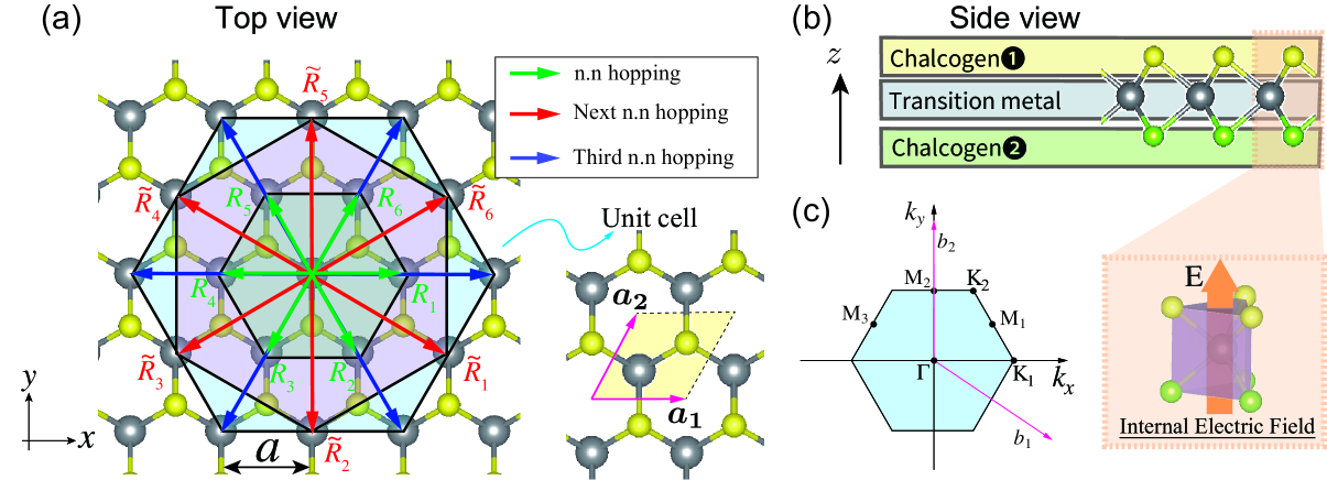
Figures 1(a) and (b) show the top and side views of monolayer Janus TMDCs, respectively. Monolayer Janus TMDCs belong to the space group , which consists of a transition metal layer sandwiched between two layers of different chalcogen atoms. Therefore, they have a hexagonal lattice structure but lack out-of-plane mirror symmetry, distinguishing them from conventional TMDCs [Fig. 1(b)]. This unique structure generates an internal electric field perpendicular to the materials. Additionally, Fig. 1(a) shows the unit cell (the yellow shaded rhombus). Here, the magenta arrows are primitive vectors, given as and , where is the lattice constant: Å. Since the corresponding reciprocal lattice vectors are given as and , the first BZ of monolayer TMDCs form a hexagonal shape as shown in Fig. 1(c).
II.2 Hamiltonian
For WSeTe, we employ a multiorbital TBM that includes , , and orbitals of the W atom to describe the low-energy electronic states of monolayer Janus TMDCs [35, 36, 37]. The eigenvalue equation of the effective TBM is
| (1) |
where is the wave-number vector, is the eigenvalue and denotes the band index. The eigenvector is defined as
| (2) |
where indicates the transpose of the vector and means the amplitude at atomic orbital with spin for the th energy band at . The Hamiltonian with the Ising-type and Rashba-type SOCs can be written as
| (3) |
with
| (4) |
| (5) |
and
| (6) |
Here, and represent a and identity matrix, respectively. is -component of Pauli matrices () and is the Ising-type SOC parameter. For monolayer WSeTe, we use . Note that we adopt the Ising-type SOC parameter from WSe2 as reported in previous work [35]. Although WSeTe is a Janus material with broken out-of-plane symmetry, its underlying electronic structure associated with Ising-type SOC remains largely similar to that of WSe2. Previous studies have shown that Ising-type SOC is robust and only slightly affected by the formation of a Janus structure [36].
The first term in Eq. (3) represents the spin-independent component. includes the electron hoppings only among three orbitals of transition metal atoms, which are assumed up to third-nearest neighbor (NN) sites. As shown in Fig. 1(a), green, red, and blue arrows indicate hopping vectors pointing to NN sites, the vectors pointing to next-NN sites, and the vectors pointing to third-NN sites, respectively. The details of matrix elements , , , , , and can be found in Appendix A. The second term of Eq. (3) corresponds to the Ising-type SOC, which arises from atomic spin-orbit interaction. In the third term of Eq. (3), denotes the chemical potential. The fourth term of Eq. (3), , represents the Rashba-type SOC, which arises due to the breaking of out-of-plane mirror symmetry. denotes the parameter that represents the effective Rashba-type SOC strength for {}. In this paper, we set to for WSeTe, a value that has been validated in previous studies on Janus TMDCs [36]. Rashba-type SOC for the {} is neglected because the spin splitting induced by Rashba-type SOC occurs mainly in the valence band around the point, which is dominated by the orbitals [35, 36, 31]. If we define , the functions and are given by
| (7) | ||||
| (8) |
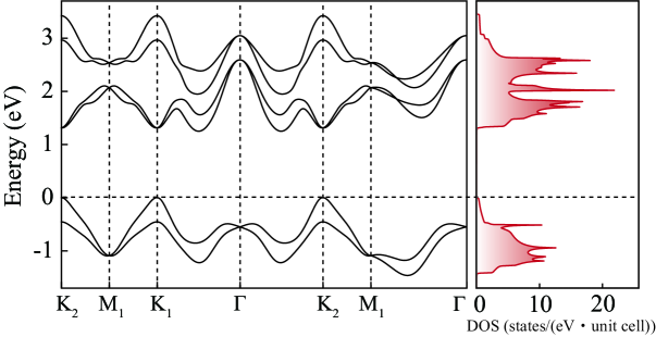
Figure 2 shows the energy band structure of monolayer WSeTe along the line passing through the high-symmetry points of the first Brillouin zone (BZ) and the corresponding density of states (DOS). Here, valence-band maximum at -point is set to zero. Monolayer WSeTe is a semiconductor with a direct band gap of eV at the and points.
II.3 Spin-polarized Fermi lines of hole-doped WSeTe
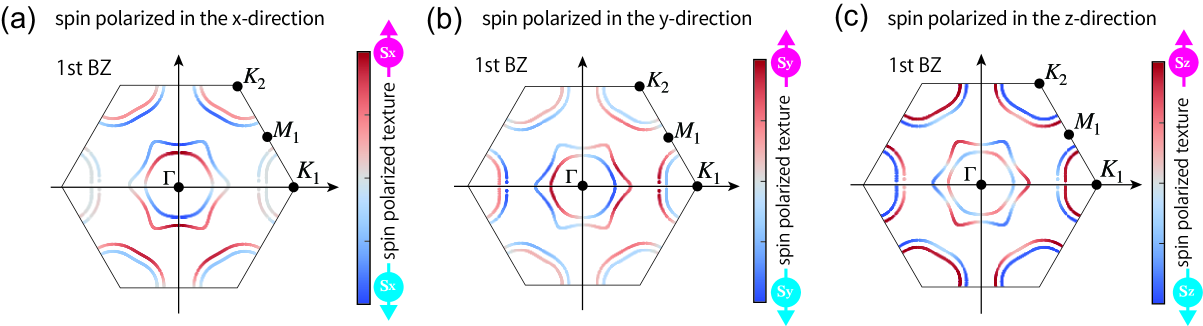
Figures 3(a)-(c) represent spin-polarized contour plots of the Fermi lines for hole-doped Janus TMDC, where the Fermi energy is set to eV. Here, the color indicates the spin polarization in (a) , (b) , and (c) -directions, respectively. Figures 3(a) and (b) illustrate the anisotropic spin polarization induced by Rashba-type SOC due to the broken out-of-plane mirror symmetry. Figure 3(c) shows the spin polarization along the out-of-plane -direction, driven by the broken inversion symmetry and strong Ising-type SOC. Conventional monolayer TMDCs exhibit spin polarization solely in the out-of-plane direction [38]. In contrast, monolayer Janus TMDCs exhibit both in-plane and out-of-plane spin polarization due to the presence of both Rashba-type and Ising-type SOCs. The coexistence of in-plane and out-of-plane spin polarization in monolayer Janus TMDCs enables versatile control of spin currents, suggesting the potential for more advanced spintronic functionalities.
III spin-dependent conductivity
In this section, we consider the spin-dependent optical conductivity of WSeTe under linearly polarized light irradiation. Here, the spin-dependent optical conductivity is numerically calculated using Kubo formula based on an effective TBM. [39, 40, 41, 42, 43, 44, 45, 46, 47, 48] Under the application of an external electric field () to the system, the linear response of the spin current can be expressed as
| (9) |
where the is the spin-dependent optical conductivity tensor for optical angular frequency . The superscript indicates the direction of spin polarization. Thus, the spin current flowing along direction with the spin polarization can be expressed as
| (10) |
with
| (11) |
with
| (12) |
and
| (13) |
where indicates the band index including spin degree of freedom and is the eigen function of the eigen energy . represents the Fermi-Dirac distribution function which is given by
| (14) |
where is the Boltzmann constant and is the temperature. is an infinitesimally small real number. Throughout this paper, eV is set for the calculation of conductivity. Note that the specific k-point (1000 1000) and the chosen value were determined by convergence tests. denotes integration over the first BZ. is the -dependent spin current operator, which is defined as
| (15) |
which is given by the anticommutation between the group velocity operator and -component of the Pauli matrix (). Here, is the identity matrix. Equation (11) can be rewritten as
| (16) |
with
| (17) |
where is an integrand of spin-dependent optical conductivity [48].
III.1 DC Limit
In the limit of direct current (DC), i.e., at zero temperature () of the clean system ( eV), Eq. (17) can be rewritten as the spin Berry curvature [38], i.e.,
| (18) |
Here, indicates that direction is perpendicular to direction. The spin Berry curvature induces an anomalous velocity
| (19) |
under the presence of an electric field . Here, the spin Berry curvature vector is given by .
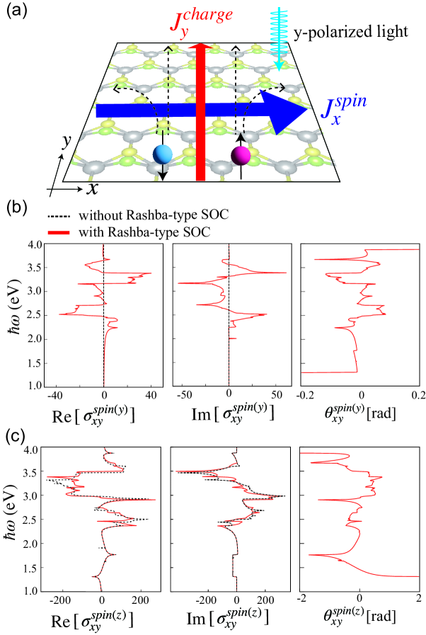
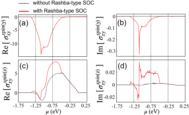
Figure 4 shows the Fermi energy dependence of spin Hall conductivity for different spin polarized directions, with (red line) and without (black dashed line) Rashba-type SOC. Since is a complex function, we can separate it into real and imaginary parts as
| (20) |
Figure 4(a) shows the real part of spin Hall conductivity, , which generates the pure spin Hall current with -polarized spin, highlighting that the inclusion of Rashba-type SOC generates in-plane spin-polarized conductivities. Figure 4(b) displays the corresponding imaginary part, . Figure 4(c) illustrates the real part of spin Hall conductivity, , to generate the pure spin Hall current with -polarized spin, which appears even without Rashba-type SOC. Figure 4(d) shows the corresponding imaginary part, . Although the -polarized pure spin Hall current is generated by the Ising-type SOC, the presence of Rashba-type SOC further enhances it.
In addition, the other components of the conductivity are calculated as follows: , , and . In Appendix B, we provide the detail for the symmetry of Berry curvature and spin Berry curvature in the 1st BZ.
These results reveal the effects of Rashba-type SOC on the generation and modulation of the spin Hall currents in monolayer Janus TMDCs. In TMDCs such as WSe2, where Rashba-type SOC is typically negligible, the spin Hall current exhibits only out-of-plane polarization. In contrast, the broken out-of-plane symmetry in Janus TMDCs such as WSeTe leads to a significant Rashba-type SOC. Rashba-type SOC plays a crucial role for generating in-plane polarized pure spin Hall current and enhancement of out-of-plane polarized pure spin hall current. These results contribute to the development of spintronic devices. Notably, the generation of the pure spin Hall current is further enhanced by hole doping.
III.2 Optical Conductivity
Next, we examine the angular frequency dependence of for monolayer WSeTe. Figure 5(a) schematically illustrates the numerical results that the optical generation of pure spin Hall current in -direction under the irradiation of -polarized light which drives a charge current along the -direction. The left and center panels of Fig. 5(b) show the real and imaginary part of spin-dependent optical Hall conductivity , i.e., the generation of spin Hall current with -polarized spin. The red lines show the results with Rashba-type SOC, while the black dot lines represent the case without it. This result indicates that the Rashba-type SOC plays a crucial role for generating in-plane spin-polarized current by irradiating linearly polarized light. The left and center panels of Fig. 5(c) illustrate the real and imaginary part of spin-dependent optical Hall conductivity , i.e., the generation of spin Hall current with -polarized spin. In this case, the conductivity remains finite even without Rashba-type SOC due to the presence of Ising-type SOC.
By considering crystal symmetry and Neumann’s principle, we can obtain the other components of conductivity tensor as follows: , , and . The detail is summarized in Appendix C.
Here we shall pay attention to the polarization direction of the generated spin Hall current. In the conventional SHE, a transverse spin current is induced in response to a charge current , where the spin polarization direction is perpendicular to both, i.e., (). However, the spin Hall currents in WSeTe are not constrained by this conventional relation. We classify these SHEs into the following types: (i) conventional SHE, where , and are mutually orthogonal, i.e., , corresponding to Fig. 5(c); (ii) in-plane SHE (IPSHE), where and are transverse, but is parallel to one of them, i.e., or , corresponding to Fig. 5(b).
Furthermore, we consider the angular frequency dependence of the spin Hall angle (SHA) [49], which measures the conversion efficiency from charge current to spin current. SHA can be given as
| (21) |
where represents the spin-dependent optical conductivity, is the optical longitudinal conductivity. The factor ensures that the units of spin conductivity match those of charge conductivity. The right panels of Figs. 5(b) and (c) show SHA of monolayer WSeTe for different spin polarization direction: (b) -direction and (c) -direction . Each SHA has divergence at approximately 1.2 eV and 3.9 eV due to becoming zero, making SHA ill-defined. When the spin-dependent optical conductivity reaches a peak in the left panels of Figs. 5(b) and (c), the SHA also increases, indicating that spin current can be generated efficiently.
In Appendix D, we derive the optically generated spin current by circularly polarized light irradiation. In Appendix E, we examine the temperature dependence of the spin-dependent optical Hall conductivity. Our finding indicates that the spin-dependent optical Hall conductivity is robust against temperature variations and is expected to be observable even at room temperature.
IV conclusion
In this study, we have theoretically demonstrated the generation of pure spin Hall current in monolayer WSeTe under linearly polarized light irradiation. Monolayer WSeTe possesses both Ising-type SOC and Rashba-type SOC due to broken out-of-plane mirror symmetry. These SOCs induce the finite spin Berry curvature, resulting in the generation of the spin Hall effect by light irradiation. In particular, the presence of Rashba-type SOC induces in-plane polarized spin-dependent optical conductivities, giving rise to unconventional spin Hall effects,. i.e., IPSHE. IPSHE enables direct control of the spin polarization direction within the plane of the monolayer. Thus, monolayer WSeTe can be utilized for the source of pure spin Hall current and next-generation opt-spintronics devices such as in-plane spin injection, detection and manipulation under linearly polarized light using IPSHE, where conventional SHE is less optimal. In addition, we have calculated SHA, which measures conversion efficiency from charge current to spin Hall current. The results show that each SHA is enhanced by irradiating visible light.
Our results offer a new degree of freedom for designing optospintronic devices, such as spin current harvesting via light irradiation in 2D materials.
ACKNOWLEDGMENTS
This work was supported by JSPS KAKENHI (Grants No. JP25K01609, No. JP22H05473, and No. JP21H01019), JST CREST (Grant No. JPMJCR19T1). K. W. acknowledges the financial support for Basic Science Research Projects (Grant No. 2401203) from the Sumitomo Foundation. Sasakawa Scientific Research Grant from The Japan Science Society.
Data Availability
The data that support the findings of this study are available from the corresponding author upon reasonable request [50].
Appendix A Matrix Elements of Monolayer WSeTe
In Sec. II, we introduced the effective hamiltonian of monolayer WSeTe given by Eq.(4). Here we provide the details of matrix elements, i.e., and . These elements are expressed as follows.
The specific hopping parameters in this TBM can be given as:
| (22) |
where indicates an atomic orbital of the W atom, and in this paper, we consider , , and . Here, we define , , , , , and . The fitted parameters are summarized in Table 1.
| WSeTe | 0.728 | 1.655 | -0.146 | -0.124 | 0.507 | 0.117 | 0.127 | 0.015 | 0.036 | -0.234 | 0.107 |
| 0.044 | 0.075 | -0.061 | 0.032 | 0.007 | 0.329 | -0.202 | -0.164 | 0.228 | 0.045 |
Appendix B Symmetry Analysis of the Integrands for charge and spin-dependent Conductivities
In Sec. III, we calculated spin-dependent optical conductivities, integrating Eq. (17) over the first BZ. In a similar manner, here we shall focus on the integrand of the charge conductivity. In the DC limit, the integrand can be represented as
| (23) |
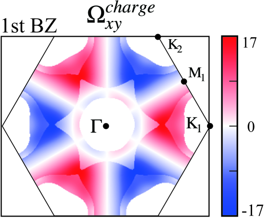
For , this is nothing more than the Berry curvature. Figure 6 provides counter plots of , i.e., the Berry curvature, at an energy level of -0.85 eV. The point-group symmetry of the berry curvature is and the Mulliken notations for irreducible representation (IR) is . Notably, indicates that the berry curvature antisymmetric under the symmetry operations of the point group, vanishing of the total integral over the BZ. Thus, the charge Hall conductivity becomes identically zero, although this is trivial from that the system has the time-reversal symmetry.
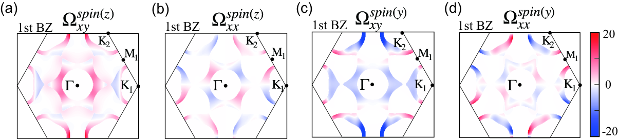
Similarly, we can analyze the symmetry of spin Berry curvature in the first BZ. Figure 7(a) shows , i.e., the spin Berry curvature for spin polarized along the -axis. Figure 7(b) shows , which is the integrand of longitudinal spin-dependent conductivity for spin polarized along the -axis. Figure 7(c) shows , i.e., the spin Berry curvature for spin polarized along the -axis. Figure 7(d) shows , which is the integrand of longitudinal spin-dependent conductivity for spin polarized along the -axis. The charge and spin-dependent conductivities are obtained by integrating these integrands over the first BZ.
Table 2 shows the point-group symmetries of the spin Berry curvatures presented in Fig. 7. In this table, and represent the Mulliken notations for IRs of the relevant point groups. Notably, indicates that spin Berry curvatures becomes antisymmetric under the symmetry operations, leading to the vanishing the total integral over the BZ.
| (a) | (b) | (c) | (d) | |
|---|---|---|---|---|
| point group | ||||
| IRs | ||||
| Integrated value over BZ | Finite | 0 | Finite | 0 |
Appendix C Neumann’s Principle Analysis on Spin-Dependent Conductivity Tensor
In this section, we discuss the elements of spin-dependent conductivity tensor by using the Neumann’s principle. According to Neumann’s principle, the symmetry group governing any physical property of a crystal must include all symmetry operations of the crystal’s point group. Note that because the spin operator is a pseudovector while the velocity operator is a polar vector, their combination yields a third-rank pseudotensor for the spin-dependent conductivity, i.e., spin-dependent conductivity tensor can be represented a third rank pseudo-tensor ().
The crystal symmetry of monolayer TMDCs with the point group is characterized by a three-fold rotational axis () perpendicular to the plane of the layers and a horizontal mirror plane () that lies parallel to the layers. In contrast, monolayer Janus TMDCs break the out-of-plane mirror symmetry due to the different calcogens on each side of the transition metal layer, changing the point group to . The point group retains the three-fold rotational symmetry but lacks the horizontal mirror plane symmetry. The full set of symmetry operations for is:{}, where is the identity operation, is the rotation by around the axis, is the reflection by the plane perpendicular to the plane and through the angular bisector of and in Fig. 1(a), and and are obtained by rotating around axis by and respectively.
The spin-dependent conductivity tensor can be represented as
| (24) |
where indicates the direction of spin polarization. According to the Neumann’s principle, the spin-dependent conductivity tensor can be expressed in terms of the symmetry operation matrix as ,
det() is a manifestation of the psudotensor. By considering the symmetry of the crystal, we can reduce the number of independent elements in the spin-dependent conductivity tensor. Especially, Janus TMDCs have the following symmetries: (1) (a vertical mirror plane with the mirror axis along the -axis) and (2) (a threefold rotational symmetry). Since the operator of is written as
the spin-dependent conductivity tensor can be simplified as
Similarly, since operator of is written as
we can obtain the following relations:
Thus, the following relation is deduced,
Consequently, the spin-dependent conductivity tensor can be represented as
| (25) |
| (26) |
| (27) |
where the conductivity components in the -direction are omitted, because we are considering a 2D system. Here, the conditions for these tensor elements are consistent with our numerical calculations of spin-dependent conductivities.
Appendix D Spin Current Induced by Circularly Polarized Light
Here we extend our symmetry analysis to the case of circularly polarized light [34, 47, 51]. Spin current in the direction with spin component can be given by [51]
where . The interaction matrix element, , is given by
where is the group velocity operator vector and is an external electric field. Therefore, the spin current can be rewritten as
For a right-handed circularly polarized (RCP) light, the electric field can be expressed as
| (28) |
Similarly, for left-handed circularly polarized (LCP) light, the electric field is expressed as
| (29) |
Then, the spin current flowing along direction with the spin polarization -axis can be expressed as
| (30) |
| (31) |
where the subscript () sign corresponds to RCP (LCP) and is the amplitude of the electric field.
In Janus TMDCs, the spin-dependent conductivity tensor satisfies the relations given in Eqs. (25)-(27). Consequently, the spin current can be rewritten in terms of the spin-dependent conductivity tensor as follows:
This approach provides a systematic method to predict the behavior of the spin current for various polarization states.
Appendix E Temperature Dependence of Spin-Dependent Optical Hall Conductivity
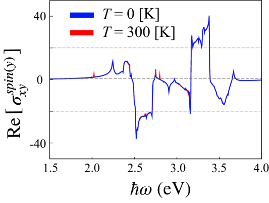
In this section, we discuss the temperature dependence of the spin-dependent optical Hall conductivity. Figure 8 shows the temperature dependence of the real part of spin-dependent optical Hall conductivity, , for monolayer WSeTe at two different temperatures. The blue line represents the result at K, while the red line corresponds to K. Our results demonstrate that the spin-dependent optical Hall conductivity is robust against temperature, indicating that it can be observable even at room temperature.
References
- Novoselov et al. [2005] K. S. Novoselov, D. Jiang, F. Schedin, T. J. Booth, V. V. Khotkevich, S. V. Morozov, and A. K. Geim, Two-dimensional atomic crystals, Proc. Natl. Acad. Sci. U.S.A. 102, 10451 (2005).
- Manzeli et al. [2017] S. Manzeli, D. Ovchinnikov, D. Pasquier, O. V. Yazyev, and A. Kis, 2D transition metal dichalcogenides, Nat. Rev. Mater. 2, 17033 (2017).
- Mak et al. [2014] K. F. Mak, K. L. McGill, J. Park, and P. L. McEuen, The valley Hall effect in MoS2 transistors, Science 344, 1489 (2014).
- Lv et al. [2015] R. Lv, J. A. Robinson, R. E. Schaak, D. Sun, Y. Sun, T. E. Mallouk, and M. Terrones, Transition Metal Dichalcogenides and Beyond: Synthesis, Properties, and Applications of Single- and Few-Layer Nanosheets, Acc. Chem. Res. 48, 56 (2015).
- Radisavljevic et al. [2011] B. Radisavljevic, A. Radenovic, J. Brivio, V. Giacometti, and A. Kis, Single-layer MoS2 transistors, Nat. Nanotechnol. 6, 147 (2011).
- Mak et al. [2010] K. F. Mak, C. Lee, J. Hone, J. Shan, and T. F. Heinz, Atomically Thin MoS2: A New Direct-Gap Semiconductor, Phys. Rev. Lett. 105, 136805 (2010).
- Mak and Shan [2016] K. F. Mak and J. Shan, Photonics and optoelectronics of 2D semiconductor transition metal dichalcogenides, Nat. Photonics 10, 216 (2016).
- Wang et al. [2012] Q. H. Wang, K. Kalantar-Zadeh, A. Kis, J. N. Coleman, and M. S. Strano, Electronics and optoelectronics of two-dimensional transition metal dichalcogenides, Nat. Nanotechnol. 7, 699 (2012).
- Splendiani et al. [2010] A. Splendiani, L. Sun, Y. Zhang, T. Li, J. Kim, C.-Y. Chim, G. Galli, and F. Wang, Emerging Photoluminescence in Monolayer MoS2, Nano Lett. 10, 1271 (2010).
- Wolf et al. [2001] S. A. Wolf, D. D. Awschalom, R. A. Buhrman, J. M. Daughton, S. v. Molnár, M. L. Roukes, A. Y. Chtchelkanova, and D. M. Treger, Spintronics: A Spin-Based Electronics Vision for the Future, Science 294, 1488 (2001).
- Long et al. [2019] M. Long, P. Wang, H. Fang, and W. Hu, Progress, Challenges, and Opportunities for 2D Material Based Photodetectors, Adv. Funct. Mater. 29, 1803807 (2019).
- Tongay et al. [2012] S. Tongay, J. Zhou, C. Ataca, K. Lo, T. S. Matthews, J. Li, J. C. Grossman, and J. Wu, Thermally Driven Crossover from Indirect toward Direct Bandgap in 2D Semiconductors: MoSe2 versus MoS2, Nano Lett. 12, 5576 (2012).
- Gutiérrez et al. [2013] H. R. Gutiérrez, N. Perea-López, A. L. Elías, A. Berkdemir, B. Wang, R. Lv, F. López-Urías, V. H. Crespi, H. Terrones, and M. Terrones, Extraordinary Room-Temperature Photoluminescence in Triangular WS2 Monolayers, Nano Lett. 13, 3447 (2013).
- Zhao et al. [2013] W. Zhao, Z. Ghorannevis, L. Chu, M. Toh, C. Kloc, P.-H. Tan, and G. Eda, Evolution of Electronic Structure in Atomically Thin Sheets of WS2 and WSe2, ACS Nano 7, 791 (2013).
- Zhu et al. [2011] Z. Y. Zhu, Y. C. Cheng, and U. Schwingenschlögl, Giant spin-orbit-induced spin splitting in two-dimensional transition-metal dichalcogenide semiconductors, Phys. Rev. B 84, 153402 (2011).
- Lu et al. [2015] J. M. Lu, O. Zheliuk, I. Leermakers, N. F. Q. Yuan, U. Zeitler, K. T. Law, and J. T. Ye, Evidence for two-dimensional Ising superconductivity in gated MoS2, Science 350, 1353 (2015).
- Zhou et al. [2016] B. T. Zhou, N. F. Q. Yuan, H.-L. Jiang, and K. T. Law, Ising superconductivity and Majorana fermions in transition-metal dichalcogenides, Phys. Rev. B 93, 180501 (2016).
- He et al. [2018] W.-Y. He, B. T. Zhou, J. J. He, N. F. Q. Yuan, T. Zhang, and K. T. Law, Magnetic field driven nodal topological superconductivity in monolayer transition metal dichalcogenides, Commun. Phys. 1, 40 (2018).
- Kormányos et al. [2014] A. Kormányos, V. Zólyomi, N. D. Drummond, and G. Burkard, Spin-Orbit Coupling, Quantum Dots, and Qubits in Monolayer Transition Metal Dichalcogenides, Phys. Rev. X 4, 011034 (2014).
- Qian et al. [2014] X. Qian, J. Liu, L. Fu, and J. Li, Quantum spin Hall effect in two-dimensional transition metal dichalcogenides, Science 346, 1344 (2014).
- Feng et al. [2012] W. Feng, Y. Yao, W. Zhu, J. Zhou, W. Yao, and D. Xiao, Intrinsic spin Hall effect in monolayers of group-VI dichalcogenides: A first-principles study, Phys. Rev. B 86, 165108 (2012).
- Safeer et al. [2019] C. K. Safeer, J. Ingla-Aynés, F. Herling, J. H. Garcia, M. Vila, N. Ontoso, M. R. Calvo, S. Roche, L. E. Hueso, and F. Casanova, Room-Temperature Spin Hall Effect in Graphene/MoS2 van der Waals Heterostructures, Nano Let. 19, 1074 (2019).
- Ominato et al. [2020] Y. Ominato, J. Fujimoto, and M. Matsuo, Valley-Dependent Spin Transport in Monolayer Transition-Metal Dichalcogenides, Phys. Rev. Lett. 124, 166803 (2020).
- Lu et al. [2017] A.-Y. Lu, H. Zhu, J. Xiao, C.-P. Chuu, Y. Han, M.-H. Chiu, C.-C. Cheng, C.-W. Yang, K.-H. Wei, Y. Yang, Y. Wang, D. Sokaras, D. Nordlund, P. Yang, D. A. Muller, M.-Y. Chou, X. Zhang, and L.-J. Li, Janus monolayers of transition metal dichalcogenides, Nat. Nanotechnol. 12, 744 (2017).
- Zhang et al. [2017] J. Zhang, S. Jia, I. Kholmanov, L. Dong, D. Er, W. Chen, H. Guo, Z. Jin, V. B. Shenoy, L. Shi, and J. Lou, Janus Monolayer Transition-Metal Dichalcogenides, ACS Nano 11, 8192 (2017).
- Zhang et al. [2022] L. Zhang, Y. Xia, X. Li, L. Li, X. Fu, J. Cheng, and R. Pan, Janus two-dimensional transition metal dichalcogenides, J. Appl. Phys. 131, 230902 (2022).
- Dong et al. [2017] L. Dong, J. Lou, and V. B. Shenoy, Large In-Plane and Vertical Piezoelectricity in Janus Transition Metal Dichalchogenides, ACS Nano 11, 8242 (2017).
- Guo et al. [2017] Y. Guo, S. Zhou, Y. Bai, and J. Zhao, Enhanced piezoelectric effect in Janus group-III chalcogenide monolayers, Appl. Phys. Lett. 110, 163102 (2017).
- Jin et al. [2018] H. Jin, T. Wang, Z.-R. Gong, C. Long, and Y. Dai, Prediction of an extremely long exciton lifetime in a Janus-MoSTe monolayer, Nanoscale 10, 19310 (2018).
- Zheng et al. [2021] T. Zheng, Y.-C. Lin, Y. Yu, P. Valencia-Acuna, A. A. Puretzky, R. Torsi, C. Liu, I. N. Ivanov, G. Duscher, D. B. Geohegan, Z. Ni, K. Xiao, and H. Zhao, Excitonic Dynamics in Janus MoSSe and WSSe Monolayers, Nano Lett. 21, 931 (2021).
- Yao et al. [2017] Q.-F. Yao, J. Cai, W.-Y. Tong, S.-J. Gong, J.-Q. Wang, X. Wan, C.-G. Duan, and J. H. Chu, Manipulation of the large Rashba spin splitting in polar two-dimensional transition-metal dichalcogenides, Phys. Rev. B 95, 165401 (2017).
- Hu et al. [2018] T. Hu, F. Jia, G. Zhao, J. Wu, A. Stroppa, and W. Ren, Intrinsic and anisotropic Rashba spin splitting in Janus transition-metal dichalcogenide monolayers, Phys. Rev. B 97, 235404 (2018).
- Chen et al. [2020] J. Chen, K. Wu, H. Ma, W. Hu, and J. Yang, Tunable Rashba spin splitting in Janus transition-metal dichalcogenide monolayers via charge doping, RSC Adv. 10, 6388 (2020).
- Freimuth et al. [2021] F. Freimuth, S. Blügel, and Y. Mokrousov, Charge and spin photocurrents in the Rashba model, Phys. Rev. B 103, 075428 (2021).
- Liu et al. [2013] G. Liu, W. Shan, Y. Yao, W. Yao, and D. Xiao, Three-band tight-binding model for monolayers of group-VIB transition metal dichalcogenides, Phys. Rev. B 88, 085433 (2013).
- Zhou et al. [2019] B. T. Zhou, K. Taguchi, Y. Kawaguchi, Y. Tanaka, and K. T. Law, Spin-orbit coupling induced valley Hall effects in transition-metal dichalcogenides, Commun. Phys. 2, 26 (2019).
- Zhou et al. [2020] B. T. Zhou, C.-P. Zhang, and K. Law, Highly Tunable Nonlinear Hall Effects Induced by Spin-Orbit Couplings in Strained Polar Transition-Metal Dichalcogenides, Phys. Rev. Appl 13, 024053 (2020).
- Habara and Wakabayashi [2021] R. Habara and K. Wakabayashi, Optically induced spin current in monolayer NbSe2, Phys. Rev. B 103, L161410 (2021).
- Guo et al. [2005] G. Y. Guo, Y. Yao, and Q. Niu, Ab initio Calculation of the Intrinsic Spin Hall Effect in Semiconductors, Phys. Rev. Lett. 94, 226601 (2005).
- Sengupta and Bellotti [2016] P. Sengupta and E. Bellotti, Intensity modulated optical transmission in a non-linear dielectric environment with an embedded mono-layer transition metal dichalcogenide, J. Appl. Phys. 120, 123105 (2016).
- Vargiamidis et al. [2014] V. Vargiamidis, P. Vasilopoulos, and G.-Q. Hai, Dc and ac transport in silicene, J. Phys. Condens. Matter 26, 345303 (2014).
- Tanaka et al. [2008] T. Tanaka, H. Kontani, M. Naito, T. Naito, D. S. Hirashima, K. Yamada, and J. Inoue, Intrinsic spin Hall effect and orbital Hall effect in 4d and 5d transition metals, Phys. Rev. B 77, 165117 (2008).
- Ferreira et al. [2011] A. Ferreira, J. Viana-Gomes, Y. V. Bludov, V. Pereira, N. M. R. Peres, and A. H. C. Neto, Faraday effect in graphene enclosed in an optical cavity and the equation of motion method for the study of magneto-optical transport in solids, Phys. Rev. B 84, 235410 (2011).
- Morimoto et al. [2009] T. Morimoto, Y. Hatsugai, and H. Aoki, Optical Hall Conductivity in Ordinary and Graphene Quantum Hall Systems, Phys. Rev. Lett. 103, 116803 (2009).
- Yao et al. [2004] Y. Yao, L. Kleinman, A. H. MacDonald, J. Sinova, T. Jungwirth, D.-s. Wang, E. Wang, and Q. Niu, First Principles Calculation of Anomalous Hall Conductivity in Ferromagnetic bcc Fe, Phys. Rev. Lett. 92, 037204 (2004).
- Li and Carbotte [2012] Z. Li and J. P. Carbotte, Longitudinal and spin-valley Hall optical conductivity in single layer MoS2, Phys. Rev. B 86, 205425 (2012).
- Akita et al. [2020] M. Akita, Y. Fujii, M. Maruyama, S. Okada, and K. Wakabayashi, Momentum-selective optical absorption in triptycene molecular membrane, Phys. Rev. B 101, 085418 (2020).
- Qiao et al. [2018] J. Qiao, J. Zhou, Z. Yuan, and W. Zhao, Calculation of intrinsic spin Hall conductivity by Wannier interpolation, Phys. Rev. B 98, 214402 (2018).
- Tao et al. [2018] X. Tao, Q. Liu, B. Miao, R. Yu, Z. Feng, L. Sun, B. You, J. Du, K. Chen, S. Zhang, L. Zhang, Z. Yuan, D. Wu, and H. Ding, Self-consistent determination of spin Hall angle and spin diffusion length in Pt and Pd: The role of the interface spin loss, Sci. Adv. 4, eaat1670 (2018).
- Kameda and Wakabayashi [2025] T. Kameda and K. Wakabayashi, Research data for ”optically induced spin hall current in janus transition-metal dichalcogenides” (2025), available from the corresponding author upon reasonable request.
- Xu et al. [2021] H. Xu, H. Wang, J. Zhou, and J. Li, Pure spin photocurrent in non-centrosymmetric crystals: bulk spin photovoltaic effect, Nat. Commun. 12, 4330 (2021).