Diverse electronic phases correlated with twist-angle distribution and pseudomagnetic field in turbostratic graphene
Abstract
Twisted multilayer graphene has become a focal point of research due to its ability to host a range of quantum phases, including unconventional superconductivity, ferromagnetism, and strong correlation effects. In the present work, we address the challenge of investigating the diverse physics associated with a variety of twist-angles in a simple graphene platform which is economic and bypasses the tedious process of fabricating multiple devices, each with one twist angle. We used turbostratic graphene films containing a variety of twist angles characterized by distinct Moiré patterns observed through scanning tunneling microscopy (STM), and distinct signatures recorded by Raman spectroscopy. From scanning tunneling spectroscopy (STS), we show that the local twist-angles remarkably correlate with the characteristic local electronic properties. Most remarkably, the films spontaneously generate strained wrinkles during growth, with certain wrinkled regions exhibiting robust strain-induced pseudo-magnetic fields, as recorded by ultra-low temperature STS.
I Introduction
In twisted multilayer graphene, by tuning the twist angle between the respective monolayers, it is possible to achieve a plethora of quantum phases displaying fascinating physical properties including strongly correlated many-body physics and seemingly unconventional superconductivity Chen et al. (2019); Sharpe et al. (2019); Chen et al. (2020); Serlin et al. (2020); Polshyn et al. (2020); Cao et al. (2018a); Dean et al. (2013); Hunt et al. (2013); Cao et al. (2018b); Luican et al. (2011); Ohta et al. (2012); Yin et al. (2016); Finocchiaro et al. (2017); Stauber et al. (2018). Inspired by such discoveries, attempts are being made to tune the twist angle more precisely and over larger ranges to explore the possibility of even richer physics. However, such fine control over a large range of twist angles is an extremely challenging task that involves the fabrication of multiple devices for each given twist angle. Here we show that a large number of twist angles can be obtained in a single large-area film of turbostratic graphene that is far easier to fabricateMogera et al. (2015). Unlike regular multilayer graphene which has a definite inter-layer stacking, turbostratic graphene hosts a distribution of local stacking pattern Lenski and Fuhrer (2011); Garlow et al. (2016); Kokmat et al. (2023). In addition, in turbostratic graphene, the stacked layers are effectively decoupled over a major fraction of the film area and have a larger interlayer separation. Raman spectroscopy measurements revealed a remarkable similarity of the top layer of a turbostratic graphene film to that of exfoliated monolayer graphene. Given this similarity and the fact that large area turbostratic graphene films can be produced in large quantities, they provide a favorable platform for the investigation of fundamental physics and the industrial application of graphene devicesGupta et al. (2022).
Using scanning tunneling microscopy we have identified various twist angles characterized by specific Moiré patterns on a series of turbostratic graphene films grown by a simple Joule heating technique. Such films also generate spontaneous wrinkles during growth. The high quality of the turbostratic films is evident from the detailed characterization of these films using Raman spectroscopy, electron diffraction, and electrical transport studies reported elsewhereMogera et al. (2017); Mogera and Kulkarni (2018); Gupta et al. (2020). In certain specific wrinkled areas tunneling spectroscopy experiments down to 350 mK revealed robust signature of pseudo-magnetic fields of varying strength. The discoveries indicate that turbostratic graphene films may find diverse applications in the broad emerging area of twistronics Hennighausen and Kar (2021); Carr et al. (2017).
II Results and discussion
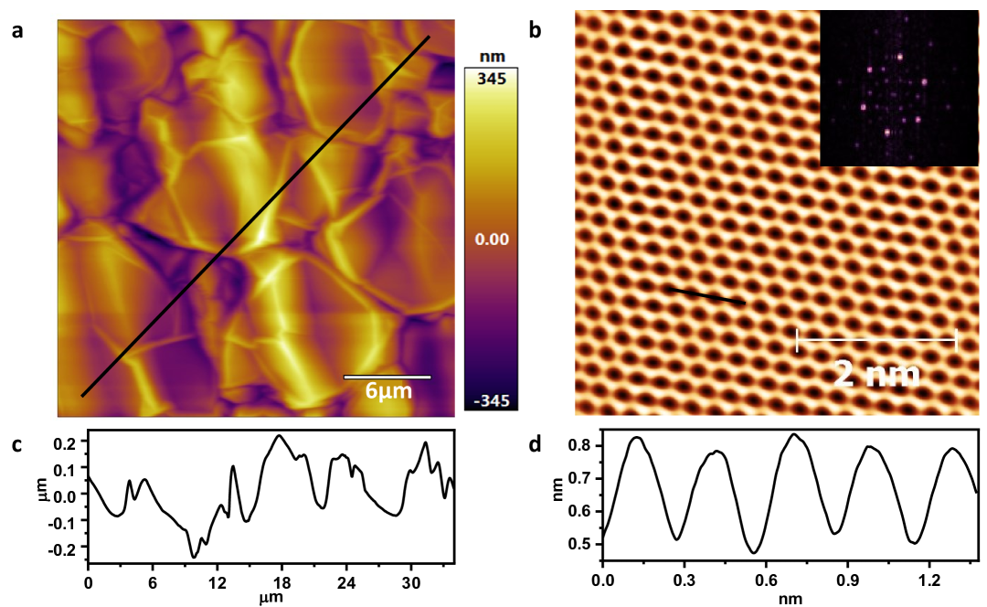
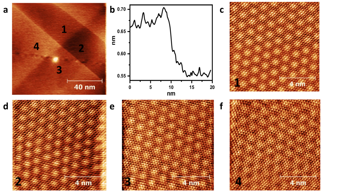
For characterization of the surface of the turbostratic graphene films, we first performed atomic force microscopy experiments at room temperature. Figure 1(a) presents an atomic force microscopy (AFM) topography that illustrates the presence of wrinkles in the film. By examining the line profile, as shown in Figure 1(c), it is evident that the wrinkles exhibit greater thickness compared to the flat regions of the film. In earlier reports, the wrinkled regions were found to be more conductive than the flat regionsMoun et al. (2021). To probe the atomic scale microscopic structure of such wrinkled regions, we performed scanning tunneling microscopy and spectroscopy (STM/S) at 77 K. A small area STM topograph of 5 5 nm2 (Figure 1 (b)) in a selected region shows the presence of a lattice with a lattice constant matching that of single layer graphene (Figure 1 (d)), indicating that these regions have top graphene layer significantly decoupled from the underlying stacking layers with high turbostraticity and that effectively behaves like suspended monolayer graphene. We found that there are different regions with varying degrees of turbostraticity and stacking patterns over the film surface. The fact that a single large area film shows a wide range of stacking twist angles as well as varying interlayer hybridization, makes the system unique.
In addition, there are regions which have considerable interlayer hopping where we found a Moiré lattice as well as spectroscopic signature of multilayer physics. We note that the spatial extent of the “coupled” regions with well-resolved Moiré patterns was, on average, of the order 1 m. This is confirmed by Raman mapping analysis as well as STM imaging over large area. In the supporting information(SI) file, in Figures S1-S4, we have shown uniformity of the Moiré patterns over large areas in different regions of the turbostratic film. The Raman mapping analysis is summarized in Figures S6 and S7.
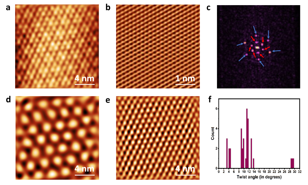
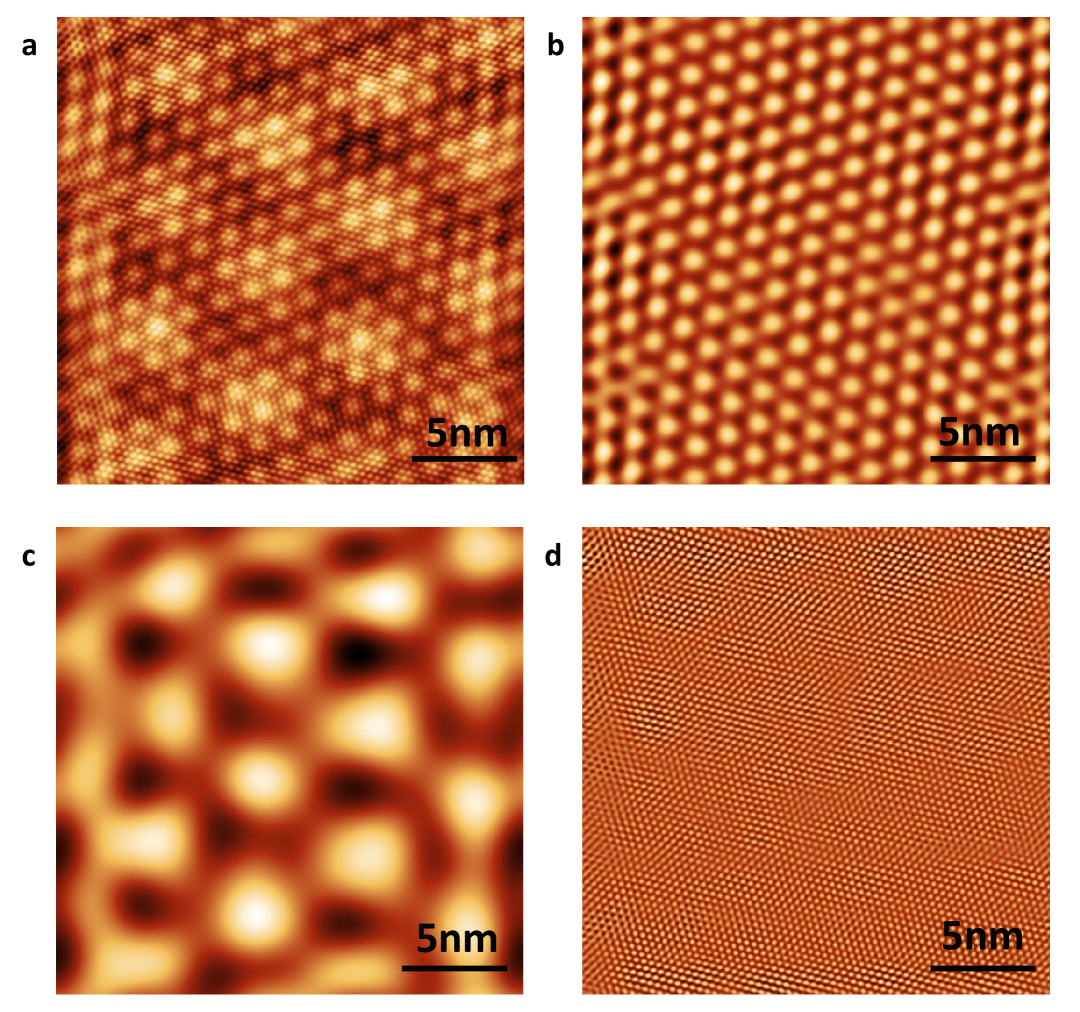
The atomic resolution image of another selected region over 19 19 nm2 area is shown in Figure 2(a). The image shows a graphene lattice as well as a complex periodic pattern of bright spots with a lattice constant different from the graphene lattice constant. Such periodic patterns arise when two or more layers of periodic lattice points with nearly matching lattice spacing are stacked with a twistChen et al. (2019); Sharpe et al. (2019); Chen et al. (2020); Serlin et al. (2020); Polshyn et al. (2020). To understand the origin of such a complex Moiré pattern, we analyzed the image digitally. First, we performed a Fast Fourier Transform(FFT) of the topographic image, shown in Figure 2(c) and then sequentially masked different regions (indicated by arrows) of the FFT image to uncover the contribution of structures with different periodicity. Figure 2(d) displays the inverse FFT of the inner regions marked by red arrows, while Figure 2(e) shows the inverse FFT corresponding to the outer regions marked by blue arrows. These figures illustrate two types of Moiré patterns characterized by different lattice constants. The twist angle between consecutive layers can be calculated using the relation ; where is the observed Moiré period, is the twist angle and is the graphene lattice constant Hermann (2012). Using this scheme, twist angles of around 4.46∘ and 10∘ were obtained for Figure 2(d) and 2(e), respectively. Two different types of Moiré pattern indicate the contribution of multiple (possibly three) twisted graphene layers. A large number of STM topographs were recorded in different regions and corresponding twist angles were calculated (please refer to the SI file for details). The statistics of the twist angles obtained are shown in Figure 2(f) which indicates that a wide range of twist angles are present in the turbostratic graphene films. The distribution also reveals that the major fraction of the turbostratic film hosts a twist angle of around 12o.
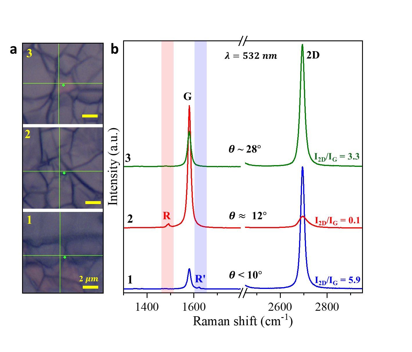
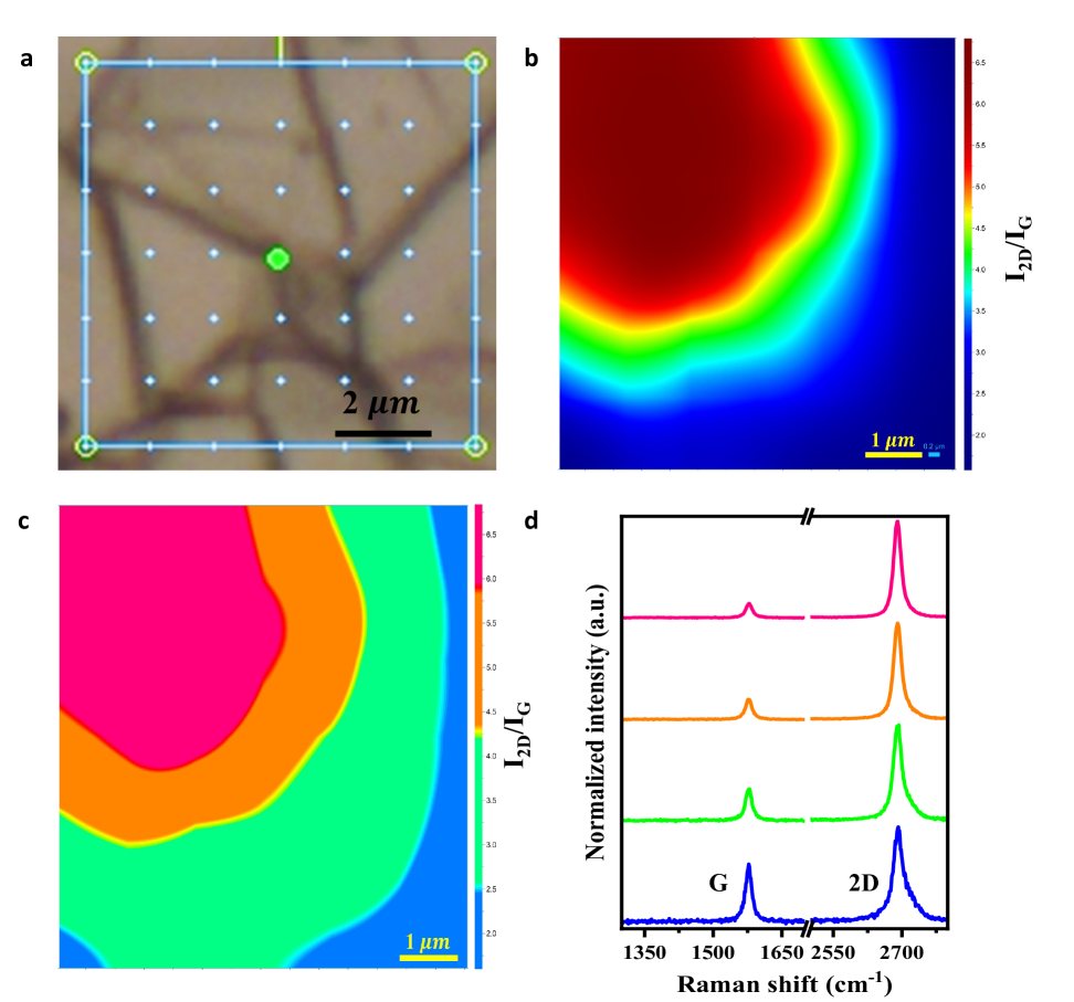
The distribution of the twist angle discussed above is also supported by our Raman spectroscopy analysis conducted on various regions of the films. In Figure 3(a) we show optical microscope images of the regions (marked by the green dots) of a graphene film where the Raman spectroscopy experiments were carried out. The corresponding Raman spectra, acquired using a 532 nm laser, are shown in Figure 3(b). The Raman spectra of all the three marked regions exhibit prominent and peaks, located at approximately 1580 cm-1 and 2695 cm-1 respectively. The spectrum labeled as 1 closely resembles the Raman signature similar to bilayer graphene with an interlayer twist angle of less than 10oSun et al. (2021). This spectrum features the rotational peak termed as peak around 1622 cm-1. However, unlike twisted bilayer graphene with a twist angle below 10o, where the intensity ratio of the 2D to G peaks (I2D/IG) is typically less than 1Sun et al. (2021); Kim et al. (2012), this region of turbostratic graphene demonstrates higher I2D/IG ratio due to the presence of more than two layersMogera et al. (2015). In the presented spectrum, I2D/IG is measured to be 5.9.
The spectrum labeled as 2 corresponds to the unique stacking arrangement in graphene layers known as the G-enhancement. This phenomenon occurs when the laser excitation energy matches the energy difference between the conduction and valence Van Hove singularitiesKim et al. (2012). For bilayer graphene with a twist angle of approximately 12o, this strong resonance is observed at a laser wavelength of 532 nm (energy = 2.33 eV)Sun et al. (2021). In the presented spectrum, the G peak is strongly enhanced compared to the 2D peak, with both peaks exhibiting a single Lorentzian profile. The presented spectrum shows I2D/IG = 0.1. This observation is consistent with our STM image analysis which also revealed a dominant existence of the twist angle of 12o. Furthermore, in spectrum 2, an additional rotational peak, termed as the peak, is observed around 1490 cm-1, with an enhanced intensity.
The spectrum labeled as 3 represents the Raman signature similar to bilayer graphene with an interlayer twist angle 28o. In this case, the 2D peak intensity exceeds the G peak. The presented spectrum reveals . Furthermore, the characteristic rotational peaks observed at smaller twist angles, the peak (associated with twist angles below 10o) and the R peak (associated with G-enhancement) are not prominently resolved in this spectrum. Therefore, in agreement with the STM results, the Raman measurements confirm the existence of a large range of twist angles between multiple layers of graphene sheets in our turbostratic graphene films.
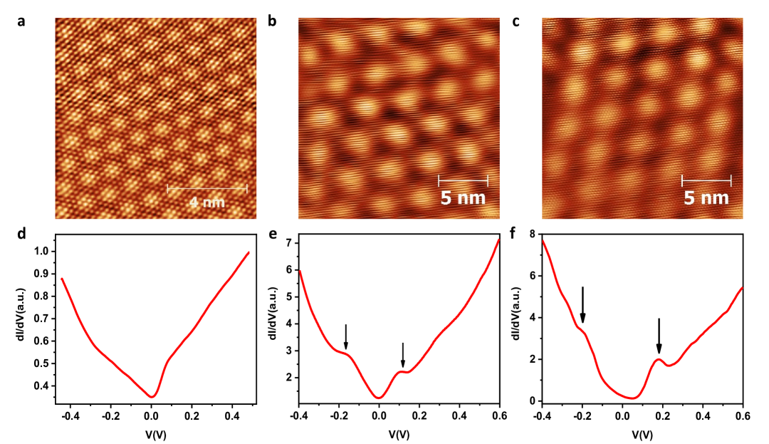
In order to explore the variety of physics that these twist angles might present, we performed scanning tunneling spectroscopy (STS) at various points on the surface of the turbostratic graphene films. Figure 4(a) depicts a 10 10 nm2 area showing a Moiré pattern with inter-layer twist angle of 14.7o. The spectroscopic measurements in the same region display Dirac cone-like linear energy dependence of the local density of states (Figure 4(d)). The existence of such a Dirac cone feature is known to arise for twisted graphene with large twist angles (>5o). In such cases, the Dirac cones corresponding to each layer are shifted in the momentum space with mutual overlapping leading to a reconstructed band structure which retains the linear dispersion for certain large twist anglesLatil et al. (2007); Hass et al. (2008); Lopes dos Santos et al. (2007); Luican et al. (2011); Shallcross et al. (2010).
For smaller twist angles, saddle point features appear in the band structure due to finite interlayer coupling. They appear as van Hove singularities (vHS)Li et al. (2010); Yan et al. (2012); Brihuega et al. (2012); Yan et al. (2014) in local density of states (LDOS) spectra. In Figure 4(b,c), we show the Moiré pattern of two different regions with twist angles of 3.4∘ and 3.5∘ respectively. For such low twist angles our STS spectra indeed revealed the vHS (Figure 4(e,f)). In these cases, we also found the evidence of angle dependent variation of the energy gap 0.28 eV and 0.37 eV in Figure 4(e,f) respectively.
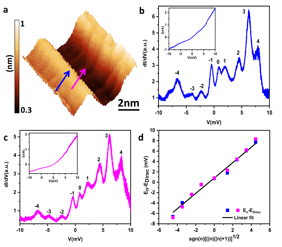
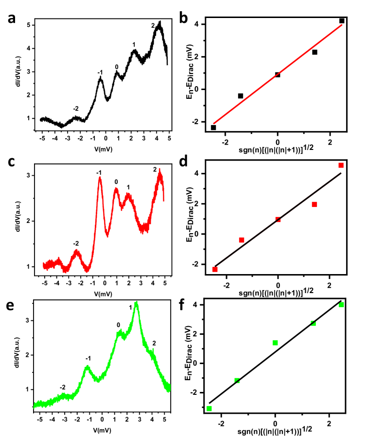
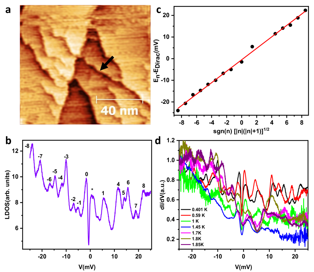
Since the turbostratic graphene films also host a distribution of strain on the surface, we performed experiments down to 400 mK to investigate the effect of the local strain field on the local electronic properties. For such experiments, we first obtained an atomically resolved topographic image of a highly strained area hosting a wrinkle (Figure 5(a)). The region over the 10 10 nm2 area shows a prominent ripple with height 0.2 nm and width 3.5 nm (estimated from the FWHM of the line profile across the ripple). The underlying graphene lattice is visible but is highly distorted and therefore the stacking order could not be resolved. The STM topograph recorded at a distance of 150 nm from the strained region (topograph in Figure 5 (a)) reveals the stacking of at least three layers of graphene (Figure S5 in the SI file). Then, we performed local spectroscopy at various points in the same region. In Figures 5(b) and 5(c), we present two representative vs spectra corresponding to the two points indicated by the blue and magenta arrows in Figure 5(a). As seen in Figure 5(b,c), a series of peaks were observed in the LDOS plot as a function of energy. The corresponding - characteristics are shown in the respective . The separation between consecutive peaks varies from 1.4 meV to 1.8 meV. These resemble the pseudo-Landau levels (PLL) induced by the coupling of the strain field with the relativistic charge carriers in grapheneMao et al. (2020); Lee et al. (2011). Starting from the charge neutrality point, we labeled the PLL peaks in terms of where is an integer. We then investigated the scaling of the energy () of the th peak with index . As shown in Figure 5(d), we found that - vary linearly with . Such a scaling behavior is known to exist for trilayer graphene Yin et al. (2015), and therefore is relevant in this case. Following the scheme presented elsewhere Yin et al. (2015); Levy et al. (2010), the expected strain-induced flux per ripple in distorted graphene is = (/) , where is the height of the ripple, is the width of the ripple, is the C-C bond length (0.142 nm), is the quantum of flux and relates the change in the hopping amplitude between nearest neighbor carbon atoms to bond length. It has a typical magnitude of 2 3 for graphene. This gives an estimate of the pseudomagnetic field 26 Tesla. This corresponds to magnetic length, 25 nm/ 4.8 nm. This is consistent with the length scale of the rippled region. The presence of high curvature of the ripples and the consequent large local strain give rise to the high local pseudomagnetic field making it possible to observe PLLs. This is consistent with the typical magnitude of PLL seen in certain 2D systems with linear bandsKamboj et al. (2019).
Next, we also performed temperature dependence of the conductance spectra displaying PLL in another region as shown in Figure S9(a) in the SI file. The LDOS spectra at 400 mK clearly show a Dirac cone-like sharp dip around zero and Landau level-like oscillations at a higher bias (Figure S9(b)). With slowly raising temperatures upto 1.85 K, we found that while the Dirac cone feature remains locked at a given energy, everywhere else the oscillations gradually smear out (Figure S9(d)). This behavior over a rather narrow temperature range (between 400 mK and 1.85 K) indicates a low Dingle temperature due to disorder in the turbostratic graphene films.
III Conclusion
Therefore, from our scanning tunneling microscopy and Raman spectroscopy experiments, we found a spontaneous distribution of a variety of twist angles between graphene layers in a single large-area film of turbostratic graphene. The tunneling spectroscopic measurements confirmed the correlation between the twist angles and the electronic properties of graphene. In addition to a rich distribution of twist angles, the turbostratic films also host a rich distribution of mechanical strain leading to topographic wrinkles. The spectroscopic measurements in certain strained areas provide direct evidence of the generation of a pseudo-magnetic field that follows a scaling behavior typical for trilayer graphene.
IV Methods
To grow a turbostratic graphene film on Nickel (Ni), a current-carrying polycrystalline nickel foil was connected to electrodes. A solution of naphthalene in chloroform was applied to the Nickel foil by dropping it onto the surface. The nickel foil was then subjected to Joule heating, reaching a high temperature of approximately 800∘C, using a direct current (DC) source with a current density of 120 . This process lasted for 15 minutes under a pressure of 4 mTorr. After heating, the nickel foil was rapidly cooled. The graphene film thus formed shows a wrinkled structure which is believed to develop during the cooling phase after the high-temperature synthesis process, primarily due to the differential contraction of the Ni substrate and graphene.
Atomic force microscopy imaging was performed at ambient (MFP 3D of Asylum Research system), in non-contact mode using a Si-cantilever. The resonance frequency of AFM probe was around 75 kHz.
STM/S measurements were performed using an ultra-low temperature and ultra-high vacuum UNISOKU USM 1300 equipped with RHK R9 controller. Before STM measurements, the sample of size 4 mm 2 mm was mounted on an Arsenic-doped Silicon chip using silver epoxy. The sample was heated - in the UHV preparation chamber by flowing current through the Si-chip to remove any oxide layer/surface contamination and then transferred to the scanning stage. Similarly, electrochemically etched Tungsten tip was cleaned inside UHV by heating treatment. STM/S measurements were performed at 77 K and 350 mK as mentioned in the main text. All the topography imaging was done in constant current mode. Gwyddion software was used for performing the Fourier transform.
The Raman spectroscopy measurements were performed using an XploRA Plus (HORIBA) Raman microscope. A 532 nm laser served as the excitation source. Spectral data were acquired using a 100 objective with a numerical aperture of 0.8. Raman mapping analysis has been done using LabSpec 6 software.
Acknowledgment:
M.G. thanks the Council of Scientific and Industrial Research (CSIR), Government of India, for financial support through a research fellowship (Award No. 09/947(0227)/2019-EMR-I). D.R. acknowledges the Department of Science and Technology, Government of India for the INSPIRE Fellowship. G.S. acknowledges financial assistance from the Science and Engineering Research Board (SERB), Govt. of India (grant number: CRG/2021/006395).
Supporting information file
Uniform twist angles over large regions; STM topograph near wrinkled region; Raman Mapping analysis; Additional Scanning tunneling spectra; Temperature dependence of conductance spectra; Distribution of Moiré lattice.
Data availability
The data that support the findings of this study are available within the article and the supporting information file.
Competing interests
The authors declare no competing financial interests.
References
- Chen et al. (2019) G. Chen, L. Jiang, S. Wu, B. Lyu, H. Li, B. L. Chittari, K. Watanabe, T. Taniguchi, Z. Shi, J. Jung, et al., Nature Physics 15, 237 (2019).
- Sharpe et al. (2019) A. L. Sharpe, E. J. Fox, A. W. Barnard, J. Finney, K. Watanabe, T. Taniguchi, M. A. Kastner, and D. Goldhaber-Gordon, Science 365, 605 (2019).
- Chen et al. (2020) G. Chen, A. L. Sharpe, E. J. Fox, Y.-H. Zhang, S. Wang, L. Jiang, B. Lyu, H. Li, K. Watanabe, T. Taniguchi, et al., Nature 579, 56 (2020).
- Serlin et al. (2020) M. Serlin, C. L. Tschirhart, H. Polshyn, Y. Zhang, J. Zhu, K. Watanabe, T. Taniguchi, L. Balents, and A. F. Young, Science 367, 900 (2020).
- Polshyn et al. (2020) H. Polshyn, J. Zhu, M. A. Kumar, Y. Zhang, F. Yang, C. L. Tschirhart, M. Serlin, K. Watanabe, T. Taniguchi, A. H. MacDonald, et al., Nature 588, 66 (2020).
- Cao et al. (2018a) Y. Cao, V. Fatemi, A. Demir, S. Fang, S. L. Tomarken, J. Y. Luo, J. D. Sanchez-Yamagishi, K. Watanabe, T. Taniguchi, E. Kaxiras, et al., Nature 556, 80 (2018a).
- Dean et al. (2013) C. R. Dean, L. Wang, P. Maher, C. Forsythe, F. Ghahari, Y. Gao, J. Katoch, M. Ishigami, P. Moon, M. Koshino, et al., Nature 497, 598 (2013).
- Hunt et al. (2013) B. Hunt, J. D. Sanchez-Yamagishi, A. F. Young, M. Yankowitz, B. J. LeRoy, K. Watanabe, T. Taniguchi, P. Moon, M. Koshino, P. Jarillo-Herrero, et al., Science 340, 1427 (2013).
- Cao et al. (2018b) Y. Cao, V. Fatemi, S. Fang, K. Watanabe, T. Taniguchi, E. Kaxiras, and P. Jarillo-Herrero, Nature 556, 43 (2018b).
- Luican et al. (2011) A. Luican, G. Li, A. Reina, J. Kong, R. R. Nair, K. S. Novoselov, A. K. Geim, and E. Y. Andrei, Physical Review Letters 106, 126802 (2011).
- Ohta et al. (2012) T. Ohta, J. T. Robinson, P. J. Feibelman, A. Bostwick, E. Rotenberg, and T. E. Beechem, Physical Review Letters 109, 186807 (2012).
- Yin et al. (2016) J. Yin, H. Wang, H. Peng, Z. Tan, L. Liao, L. Lin, X. Sun, A. L. Koh, Y. Chen, H. Peng, et al., Nature Communications 7, 10699 (2016).
- Finocchiaro et al. (2017) F. Finocchiaro, F. Guinea, and P. San-Jose, 2D Materials 4, 025027 (2017).
- Stauber et al. (2018) T. Stauber, T. Low, and G. Gómez-Santos, Physical Review Letters 120, 046801 (2018).
- Mogera et al. (2015) U. Mogera, R. Dhanya, R. Pujar, C. Narayana, and G. U. Kulkarni, The Journal of Physical Chemistry Letters 6, 4437 (2015).
- Lenski and Fuhrer (2011) D. R. Lenski and M. S. Fuhrer, Journal of Applied Physics 110, 013720 (2011).
- Garlow et al. (2016) J. A. Garlow, L. K. Barrett, L. Wu, K. Kisslinger, Y. Zhu, and J. F. Pulecio, Scientific Reports 6, 19804 (2016).
- Kokmat et al. (2023) P. Kokmat, P. Surinlert, and A. Ruammaitree, ACS Omega 8, 4010 (2023).
- Gupta et al. (2022) N. Gupta, U. Mogera, and G. U. Kulkarni, Materials Research Bulletin 152, 111841 (2022).
- Mogera et al. (2017) U. Mogera, S. Walia, B. Bannur, M. Gedda, and G. U. Kulkarni, The Journal of Physical Chemistry C 121, 13938 (2017).
- Mogera and Kulkarni (2018) U. Mogera and G. U. Kulkarni, Bulletin of Materials Science 41, 130 (2018).
- Gupta et al. (2020) N. Gupta, S. Walia, U. Mogera, and G. U. Kulkarni, The Journal of Physical Chemistry Letters 11, 2797 (2020).
- Hennighausen and Kar (2021) Z. Hennighausen and S. Kar, Electronic Structure 3, 014004 (2021).
- Carr et al. (2017) S. Carr, D. Massatt, S. Fang, P. Cazeaux, M. Luskin, and E. Kaxiras, Physical Review B 95, 075420 (2017).
- Moun et al. (2021) M. Moun, A. Vasdev, R. Pujar, K. Priya Madhuri, U. Mogera, N. S. John, G. U. Kulkarni, and G. Sheet, Applied Physics Letters 119, 033102 (2021).
- Sun et al. (2021) L. Sun, Z. Wang, Y. Wang, L. Zhao, Y. Li, B. Chen, S. Huang, S. Zhang, W. Wang, D. Pei, et al., Nature Communications 12, 2391 (2021).
- Hermann (2012) K. Hermann, Journal of Physics: Condensed Matter 24, 314210 (2012).
- Kim et al. (2012) K. Kim, S. Coh, L. Z. Tan, W. Regan, J. M. Yuk, E. Chatterjee, M. F. Crommie, M. L. Cohen, S. G. Louie, and A. Zettl, Physical Review Letters 108, 246103 (2012).
- Latil et al. (2007) S. Latil, V. Meunier, and L. Henrard, Physical Review B 76, 201402 (2007).
- Hass et al. (2008) J. Hass, F. Varchon, J. E. Millán-Otoya, M. Sprinkle, N. Sharma, W. A. De Heer, C. Berger, P. N. First, L. Magaud, and E. H. Conrad, Physical Review Letters 100, 125504 (2008).
- Lopes dos Santos et al. (2007) J. M. B. Lopes dos Santos, N. M. R. Peres, and A. H. Castro Neto, Physical Review Letters 99, 256802 (2007).
- Shallcross et al. (2010) S. Shallcross, S. Sharma, E. Kandelaki, and O. A. Pankratov, Physical Review B 81, 165105 (2010).
- Li et al. (2010) G. Li, A. Luican, J. M. B. Lopes Dos Santos, A. H. Castro Neto, A. Reina, J. Kong, and E. Y. Andrei, Nature Physics 6, 109 (2010).
- Yan et al. (2012) W. Yan, M. Liu, R.-F. Dou, L. Meng, L. Feng, Z.-D. Chu, Y. Zhang, Z. Liu, J.-C. Nie, and L. He, Physical Review Letters 109, 126801 (2012).
- Brihuega et al. (2012) I. Brihuega, P. Mallet, H. González-Herrero, G. Trambly De Laissardière, M. M. Ugeda, L. Magaud, J. M. Gómez-Rodríguez, F. Ynduráin, and J.-Y. Veuillen, Physical Review Letters 109, 196802 (2012).
- Yan et al. (2014) W. Yan, L. Meng, M. Liu, J.-B. Qiao, Z.-D. Chu, R.-F. Dou, Z. Liu, J.-C. Nie, D. G. Naugle, and L. He, Physical Review B 90, 115402 (2014).
- Mao et al. (2020) J. Mao, S. P. Milovanović, M. Anđelković, X. Lai, Y. Cao, K. Watanabe, T. Taniguchi, L. Covaci, F. M. Peeters, A. K. Geim, et al., Nature 584, 215 (2020).
- Lee et al. (2011) D. S. Lee, C. Riedl, T. Beringer, A. H. Castro Neto, K. Von Klitzing, U. Starke, and J. H. Smet, Physical Review Letters 107, 216602 (2011).
- Yin et al. (2015) L.-J. Yin, S.-Y. Li, J.-B. Qiao, J.-C. Nie, and L. He, Physical Review B 91, 115405 (2015).
- Levy et al. (2010) N. Levy, S. A. Burke, K. L. Meaker, M. Panlasigui, A. Zettl, F. Guinea, A. H. C. Neto, and M. F. Crommie, Science 329, 544 (2010).
- Kamboj et al. (2019) S. Kamboj, P. S. Rana, A. Sirohi, A. Vasdev, M. Mandal, S. Marik, R. P. Singh, T. Das, and G. Sheet, Physical Review B 100, 115105 (2019).
Supporting Information for
Diverse electronic phases correlated with twist-angle distribution and pseudomagnetic field in turbostratic graphene
Mona Garg1 Ankit Kumar2, Deepti Rana1, Anmol Arya1, Aswini R1, Umesh Waghmare2, G. U. Kulkarni2 Goutam Sheet1
Uniform Moiré lattice over a large region
In Figure S1(a), we show an STM image over a large area of 107 107 nm2 recorded at 77 K. This area captures two wrinkles almost normal to each other. The wrinkled regions span over a lateral length scale of 30 nm. Atomic resolution imaging reveals a distinct Moiré pattern. A line profile over the wrinkles shows a variation of 0.1 nm across the wrinkle (Figure S1(b)). In this region, the area on top of the wrinkles (Figure S1(c,d)) and the area around them (figure S1(e,f)) display the same Moiré pattern indicating that the wrinkled as well as the flat regions have identical inter-layer stacking and twist angles.
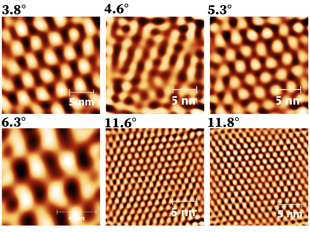
Uniform Twist angle over large regions
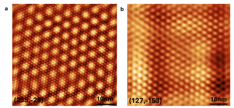
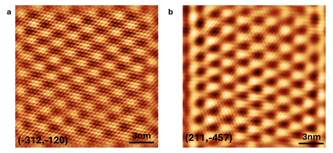
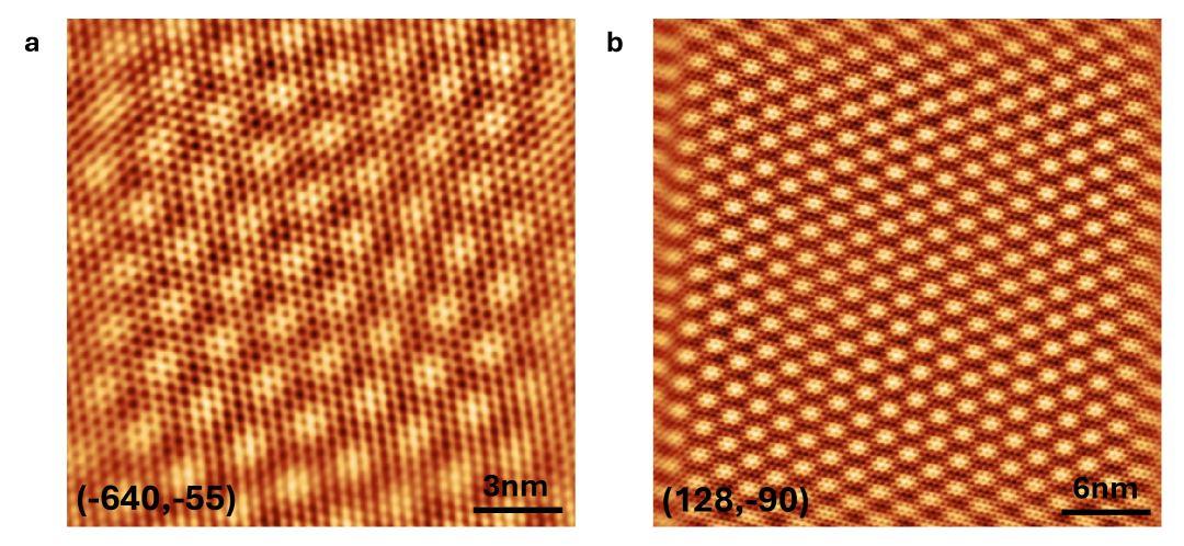
The maximum scan area that can be scanned without coarse movement in our STM is approximately 1 m. The STM topograph was analyzed in different regions to confirm the uniformity of the twist angles. The coordinates of the acquired topograph (in nm) from the center of the scan window of 1 m 1 m are noted and provided for each topograph.
STM topograph near wrinkled region
Raman mapping analysis
As characterized and described in detail in Gupta et al. (2020), the I2D/IG peak ratios from Raman spectroscopy are correlated with the twist angle distribution in twisted multilayer graphene films. The uniformity of the intensity ratio between the 2D and G peaks provides qualitative supporting evidence that the twist angle between the layers remains consistent at the micrometer scale.
Additional Scanning tunneling spectra
Temperature dependence of conductance spectra
Distribution of Moiré lattice