Ferroelectrically Switchable Chirality in Topological Superconductivity: Bilayer-MnBi2Te4/Fe(Se,Te) Heterostructure
Abstract
The interplay between ferroelectricity, magnetism, and superconductivity provides a rich platform for discovering novel quantum phenomena. Here, we propose a heterostructure composed of an antiferromagnetic bilayer MnBi2Te4 coupled with the s-wave superconductor Fe(Se,Te), enabling the realization of chiral topological superconductivity (CTSC) with switchable chirality. The chirality of the CTSC is controlled by the direction of spontaneous polarization, which arises from interlayer sliding-induced ferroelectricity or charge transfer in the bilayer MnBi2Te4. This sliding mechanism breaks the and symmetries, leading to the anomalous Hall effect in the spin-polarized metallic Dirac band and drives the emergence of CTSC when the s-wave superconductivity appears. Our work not only provides a new pathway to achieve and control topological superconductivity but also opens avenues for experimental exploration of Majorana physics and topological quantum computation.
Introduction-
The searching for the topological superconductivity[1, 2, 3, 4, 5, 6], particularly chiral topological superconductivity (CTSC)[7, 8, 9, 10, 11], has been a subject of intense research interest in recent years, due to its emergent chiral Majorana physics and potential applications in topological quantum computation and topological quantum information processing[12, 13, 14, 15, 16]. However, existing approaches to realize CTSC, such as doped topological insulators (TIs)[17, 18, 19, 20] combined with quantum anomalous Hall (QAH) systems [21, 22, 23], face significant challenges. These systems require precise fine-tuning of parameters to achieve the topologically non-trivial phase, posing a major obstacle to experimental realization and practical applications. Luckily, the recent discovery of the 2D ferroelectric materials[24, 25, 26, 27, 28], and in particular, the polar stacking bilayer MnBi2Te4[29, 30, 31, 32], offers a new opportunity to realize CTSC in a more controllable and feasible manner. Referring to the phase with spontaneous net electric polarization, ferroelectricity shares much similarity with ferromagnetism, like the tunability by external fields and symmetry breaking as the prerequisite, while differing in electric rather than magnetic, and inversion rather than time-reversal, and leads to various functional device applications[33, 34, 35]. When cooperating with magnetism, multiferroic or magnetoelectric materials[36, 37] can be realized, with coexisting ferroic orders and even couplings between, promising for intersecting manipulations. This brings us to the previously mentioned multiferroic polar stacking bilayer MnBi2Te4, which exhibits both ferroelectricity and antiferromagnetism, making it a promising platform for realizing CTSC in the proximity of superconducting pairing.
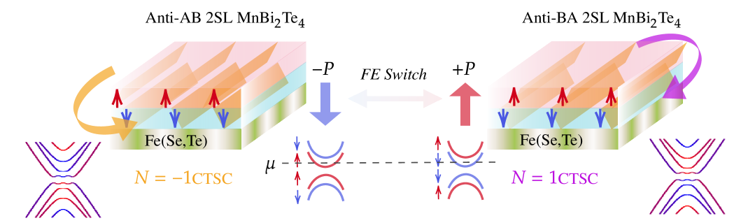
In this work, we propose the heterostructure of a polar stacking antiferromagnetic bilayer MnBi2Te4 in close proximity to an -wave superconductor Fe(Se,Te) [38, 39, 40, 41, 42]. As shown in Fig. 1, when the Fermi surface intersects a single band to form an isolated Fermi loop, this system exhibits CTSC with switchable chirality, controlled by the spontaneous polarization direction arising from the ferroelectricity induced by interlayer spin-orbital coupling due to sliding in the magnet. As we will demonstrate, this prospect is made possible by the deep cooperation between inversion -breaking ferroelectricity and antiferromagnetism in the system. We further endow a guideline for realizing of CTSC in superconducting multiferroic materials, where the Chern number of the superconducting states is determined by the residual chirality summation over all the Fermi loops: . The residual chirality of Fermi loop for band , denoted by , encodes the Fermi loop winding number with its sign of the anomalous Hall conductivity arising from all occupied states of this band, thus dictating the magnitude and direction of the Hall current[43, 44, 45].
Polar-stacking structure and ferroelectricity in bilayer MnBi2Te4-
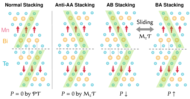
The polar-stacking structure of bilayer MnBi2Te4 arises from a mirror-twin boundary[29], where the bottom septuple layer acts as a mirror image of the top layer across the plane, accompanied with a further time-reversal operation that reverses the magnetic order and leads to the interlayer antiferromagnetism. This anti-AA stacking phase with its atomic structure is presented in Fig. 2. First-principle calculations[29] reveal four bands near the point, primarily composed of the -orbitals of Bi and Te atoms and are well-separated from others, making it feasible to construct an effective model for the system. In that sense, we consider a orbital-mixed basis for the four bands, with representing the spin-up/down states. Using the theory of invariants [46, 19, 47, 48, 49, 50], the low-energy effective Hamiltonian is given by , with
| (1) |
where , , , respectively. Here, and are the Pauli matrices acting on the layer and spin spaces, with and reading as the spin-orbital and finite-thickness coupling strengths. The last term, which we call as the quadratic warping term [51], is allowed as the second harmonic of three-fold -rotation symmetry, attributing to the absence of the inversion symmetry , which is replaced by a -mirror symmetry . Other symmetries for the construction include the time-reversal and the -mirror symmetries. Due to the ferromagnetic intra-layer and antiferromagnetic inter-layer couplings, the second part is introduced for magnetization, which preserves both and symmetries.
Finally, we let the system relax to its thermodynamically stable anti-AB or BA stacking phase, where the inter-layer sliding occurs shown schematically in Fig. 1. The realistic atomic structures are depicted in Fig. 2. This introduces the ferroelectric term
| (2) |
which breaks and simultaneously. Theoretically, this signature is evident when considering the perturbative effect of over the polarization at point. Since , its eigenstates with eigenvalue of lead to polarization aside from a length constant, where . In the weak regime, this simplifies to with , which is directly proportional, thus sign alignment and tunability. To perform numerical calculations, we put this model on a hexagonal lattice as
| (3) |
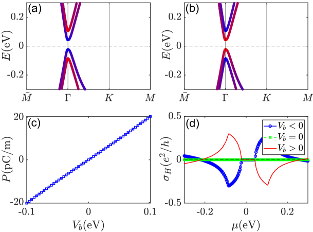
with the form of presented in Eq. (S10) of Ref.[52]. As presented in Fig. 3(c), the total polarization is almost a linear function of in a large regime, and confirms the theoretical prediction. Notably, when , we have as for a non-polarized system, representing a ferroelectric phase transition point. Note that is not a monotonic, but a periodic function of the interlayer sliding distance , and for an oversimplified illustration, we can propose thus in the linear regime.
As detailed in Sec. SII of Ref.[52], we construct a thin-film model of the bilayer system and project it onto the four lowest energy bands near the band edges [53, 54]. This reveals that the ferroelectricity term arises from interlayer spin-orbital coupling (SOC), induced by a non-trivial sliding mechanism. In the effective model, this term is referred to as the ferroelectric potential (FEP) term, distinct from external electric fields or gate-voltage effects. Physically, this additional SOC term interacts with the original -SOC and Dirac mass of the bilayer system in a non-commutative manner, creating an imbalance in the dynamics between the two layers for both spin components. This imbalance leads to charge transfer and the emergence of ferroelectricity.
Switchable anomalous Hall effect-
The interplay between antiferromagnetism and ferroelectricity in the bilayer MnBi2Te4 leads to a non-vanishing anomalous Hall effect (AHE). While interlayer sliding does not alter the band topology, the system exhibits zero Hall conductance when the chemical potential lies within the gap [29, 30, 31]. However, the ferroelectricity term breaks the symmetry, enabling the system to display an AHE when the chemical potential is shifted into the valence or conduction bands. This is confirmed by our explicit calculations of the Hall conductivity using the Kubo formula in terms of the Berry curvatures [55]. As shown in Fig. 3(d), the sign of the Hall conductance changes with different stacking configurations at a fixed Fermi level. To understand this behavior, we examine the point of the four band edges, given by . In the valence bands, the spin-up band () has a higher energy when (with by default), corresponding to the anti-AB stacking phase, and vice versa. This results in the band alignment sequences --- for the anti-AB stacking and --- for the anti-BA stacking, as shown in Fig. 3(a)(b). The spin-dependent band splitting leads to a non-compensated Berry curvature integral, resulting in the observed AHE in the conduction and valence bands. For instance, when the chemical potential lies within the higher valence band, the fully occupied lower energy bands contributes no Hall effect, while the higher energy band contributes a finite Hall conductance due to the Berry curvature integral [43, 54], with its sign determined by the spin polarization. Notably, when , corresponding to the non-polarized anti-AA stacking phase, the valence and conduction bands become degenerate, and consequently the Hall conductance vanishes. This attachment and separation of valence bands serve as a signature of the ferroelectric phase transition in this magnetic system, providing a potential experimental marker for ferroelectricity.
Chiral topological superconductivity in MnBi2Te4/Fe(Se,Te) heterostructure-
We now consider the heterostructure of bilayer MnBi2Te4 on a few-layer Fe(Se,Te), where superconductivity has been observed at the interface closely related experiment [42]. Proximity to the s-wave superconductivity in Fe(Se,Te) [38, 39, 40, 41, 42] induces a pairing potential in the bilayer MnBi2Te4, described by the Bogoliubov-de Gennes (BdG) Hamiltonian:
| (4) |
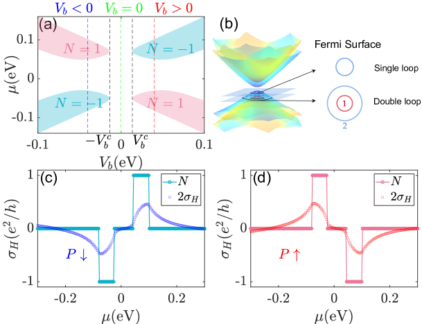
under the Nambu spinor basis, where is the chemical potential and the Pauli matrices represent the particle-hole space. For simplicity we assume a constant -wave pairing potential in the bilayer. Due to the and symmetry breaking, our particle-hole symmetric () -class system is allowed to carry a non-trivial topological index, namely the superconducting Chern number [56, 57, 58]. The possibility for the emergence of CTSC in the system is reflected by the phase boundaries defined by , which leads to the equation that where the shifted chemical potential , with . For the expression to make sense, we require and , which can be usually satisfied due to the smallness of . Under the situation, the CTSC phase appears when the self-consistent inequality is satisfied, which is shown in the phase diagram in Fig. 4(a), where two chemical potential windows emerge for each FEP intensity satisfying the above requirement. Especially, for , we have the windows as , which cannot exist either without the ferroelectricity or antiferromagnetism. In this limit, an arbitrarily small can lead to the realization of a single Fermi loop, leading to the CTSC phase. Out of the window, the double Fermi loops appear and CTSC disappears. Turning to the practical phases, we see that for the anti-AA stacking phase, and the Fermi surface always consists of two Fermi loops, consequently only trivial phase is observed when the superconducting gap open. While on the other hand, for the anti-AB/BA stacking phases shown in Fig. 4(c)(d), the superconducting Chern number changes its sign with the ferroelectric potential at a fixed Fermi level inside the observable windows, leading to a ferroelectrically switchable CTSC phase.
Coexistence of AHE and TSC-
The coexistence of the anomalous Hall effect and topological superconductivity in the system is particularly intriguing. Notably, the anomalous Hall conductance remains non-zero and non-quantized even when the system is gapped by superconductivity [59, 60, 61, 62, 63]. The Chern number is determined by the Berry curvature integrals of the occupied bands, which can be re-written using the Kubo formula evaluated over the quasi-particle current . Meanwhile, the anomalous Hall conductivity reflects the retarded electronic current response to an external electric field, which is determined by the electric correlation functions and also manifests itself as the Kubo formula, which is however evaluated over the electronic charge current , and is modified to contain only half the magnitude to compensate the Nambu space doubling. Since these two phenomena represent different physical quantities, their coexistence is not contradictory. Moreover, the superconducting pairing is typically weak, so its effect on the AHE (which does not relate to a specific topological invariant in this case) is perturbative. This allows both AHE and TSC to coexist without mutual interference, providing a unique platform for studying the interplay between these phenomena
Written under the BdG form, one can show rather generally that for the -wave pairing , indicating their relations and differences. Specifically, when we separate into the electron and hole parts (a direct sum indeed), at the same time we have , which enlightens us to write , with each part evaluated using unmodified Kubo formula over the corresponding currents. Under the limit when the electron-hole mixing fades away, the first two term equals while the last two terms vanish, leading to . Notice that the superconducting Chern number contains a singular limit, i.e., is an integer, while gives twice the anomalous Hall conductance of the normal state.
For a more intuitive picture of this coexistence, we may consider the net electron occupation number in the Bardeen-Cooper-Schrieffer (BCS) ground state relative to the electronic insulator background , with the same structure and energy spectrum, which reads and departures from zero. This implies that when the system is insulating with the chemical potential touching one band edge, the BCS state is indeed a non-fully occupied state for the electrons, allowing for the non-vanishing AHE. A more detailed discussion is presented in Sec. SV of [52].
Single loop AHE leads to CTSC-
Single or double Fermi loop of the non-superconducting system () determines topological property of the induced superconductivity (). The discussion below focuses on the limit of , but is not limited to that. The key lies in a first idealization and then a following continuous deformation of the band structure, and the fact that the topological invariant remains unchanged if the band gap does not close and reopen. When the Fermi surface crosses a single band, creating a single Fermi loop as presented in right-top of Fig. 4(b), one idealizes this crossed band (and its partner if necessary) into a regulated massless Dirac cone resembling a single surface Dirac cone of semi-magnetic TI film, which is known to carry a half-quantized anomalous Hall conductance [64, 65, 54, 50, 66] originated from the Berry phase around its Fermi loop by Stokes theorem. Importantly, this half-quantized Hall conductivity, evolves into a quantized superconducting Chern number when the system is gapped by superconductivity, [11], i.e., where the latter equality holds only in the limit of . We then let the system evolve continuously from the massless Dirac cone to the massive Dirac cone, and since the superconducting band gap at the Fermi surface survives the deformation, the quantized Chern number remains unchanged, while the second equality does not holds anymore due to the derivation from ideal massless to massive Dirac cone, . The first equality reveals the identification between superconducting Chern number and the residual chirality. Thus in general, for a single Fermi loop, the superconducting Chern number is . On the other hand, when the Fermi level crosses two bands, creating a double Fermi loop labelled by , as presented in right-bottom of Fig. 4(b), the idealization and deformation procedure tells that since the two bands carry opposite AHE, leading to the residual chirality cancellation in the two bands. See end matter for for detailed explanation and [52] SIII.4 for analytic -wave superconductivity illustration.
Discussion and summary-
Before concluding, we discuss the feasibility and broader implications of the proposed system. In the normal bulk-like stacking case (left side of Fig. 2), where the crystal orientations of the septuple layers are identical, the system either exhibits inherent symmetry for even septuple layers, or bears symmetry with vanishingly small finite-size effect. Consequently, these symmetric configurations necessarily maintain vanishing polarization, degenerate bands, and double Fermi loops. This explains why no evidence of CTSC was measured[42]. In contrast, the polar stacking with a 180∘ rotated top layer and interlayer sliding (right side of Fig. 2) breaks symmetry, leading to ferroelectricity and band splitting. The sliding occurs spontaneously, resulting in two stable configurations related by symmetry with opposite polarizations, which can be tuned by an external electric field or optical excitation[67].
The residual chirality guideline can also be generalized to multi-band systems by the summation over all the Fermi loops: , with the 1D Fermi loop winding number of th Fermi loop. In this context, we highlight several promising normal-state systems for realizing the CTSC phase. These include half-quantum Hall system[32], non-collinear antiferromagnets [68, 69], as well as collinear antiferromagnets with band splittings induced by mechanisms such as chiral crystal fields [70, 71] or charge-density-wave order [72], among others.
In summary, we have demonstrated that the multiferroic polar-stacking bilayer MnBi2Te4/Fe(Se,Te) heterostructure provides a robust and experimentally feasible platform for realizing chirality-controllable topological superconductivity.
Acknowledgements.
K.-Z. Bai acknowledges helpful discussions with S. B. Zhang. This work was supported by the Quantum Science Center of Guangdong-Hong Kong-Macao Greater Bay Area (Grant No. GDZX2301005) and the Research Grants Council, University Grants Committee, Hong Kong (Grants No. C7012-21G and No. 17301823).References
- [1] A. Y. Kitaev, Physics-Uspekhi 44, 131 (2001).
- [2] L. Fu and C. L. Kane, Phys. Rev. Lett. 100, 096407 (2008).
- [3] R. M. Lutchyn, J. D. Sau, and S. Das Sarma, Phys. Rev. Lett. 105, 077001 (2010).
- [4] X.-L. Qi and S.-C. Zhang, Rev. Mod. Phys. 83, 1057 (2011).
- [5] M. Sato and Y. Ando, Reports on Progress in Physics 80, 076501 (2017).
- [6] S.-Q. Shen, Topological insulators (Springer, 2012).
- [7] N. Read and D. Green, Phys. Rev. B 61, 10267 (2000).
- [8] F. Wilczek, Nature Physics 5, 614 (2009).
- [9] X.-L. Qi, T. L. Hughes, and S.-C. Zhang, Phys. Rev. B 82, 184516 (2010).
- [10] J. Wang, Q. Zhou, B. Lian, and S.-C. Zhang, Phys. Rev. B 92, 064520 (2015).
- [11] B. Fu and S.-Q. Shen, Phys. Rev. B 107, 184517 (2023).
- [12] S. B. Bravyi and A. Y. Kitaev, Annals of Physics 298, 210 (2002).
- [13] A. Kitaev, Annals of Physics 303, 2 (2003).
- [14] C. Nayak, S. H. Simon, A. Stern, M. Freedman, and S. Das Sarma, Rev. Mod. Phys. 80, 1083 (2008).
- [15] J. Alicea, Y. Oreg, G. Refael, F. von Oppen, and M. P. A. Fisher, Nature Physics 7, 412 (2011).
- [16] B. Lian, X.-Q. Sun, A. Vaezi, X.-L. Qi, and S.-C. Zhang, Proceedings of the National Academy of Sciences 115, 10938 (2018), https://www.pnas.org/doi/pdf/10.1073/pnas.1810003115.
- [17] L. Fu, C. L. Kane, and E. J. Mele, Phys. Rev. Lett. 98, 106803 (2007).
- [18] Y. Xia, D. Qian, D. Hsieh, L. Wray, A. Pal, H. Lin, A. Bansil, D. Grauer, Y. S. Hor, R. J. Cava, and M. Z. Hasan, Nat. Phys. 5, 398 (2009).
- [19] H. Zhang, C.-X. Liu, X.-L. Qi, X. Dai, Z. Fang, and S.-C. Zhang, Nat. Phys. 5, 438 (2009).
- [20] Y. L. Chen, J.-H. Chu, J. G. Analytis, Z. K. Liu, K. Igarashi, H.-H. Kuo, X. L. Qi, S. K. Mo, R. G. Moore, D. H. Lu, M. Hashimoto, T. Sasagawa, S. C. Zhang, I. R. Fisher, Z. Hussain, and Z. X. Shen, Science 329, 659 (2010), https://www.science.org/doi/pdf/10.1126/science.1189924.
- [21] F. D. M. Haldane, Phys. Rev. Lett. 61, 2015 (1988).
- [22] R. Yu, W. Zhang, H.-J. Zhang, S.-C. Zhang, X. Dai, and Z. Fang, Science 329, 61 (2010), https://www.science.org/doi/pdf/10.1126/science.1187485.
- [23] C.-Z. Chang, J. Zhang, X. Feng, J. Shen, Z. Zhang, M. Guo, K. Li, Y. Ou, P. Wei, L.-L. Wang, Z.- Q. Ji, Y. Feng, S. Ji, X. Chen, J. Jia, X. Dai, Z. Fang, S.-C. Zhang, K. He, Y. Wang, L. Lu, X.-C. Ma, and Q.-K. Xue, Science 340, 167 (2013), https://www.science.org/doi/pdf/10.1126/science.1234414.
- [24] M. V. Stern, Y. Waschitz, W. Cao, I. Nevo, K. Watanabe, T. Taniguchi, E. Sela, M. Urbakh, O. Hod, and M. B. Shalom, Science 372, 1462 (2021), https://www.science.org/doi/pdf/10.1126/science.abe8177.
- [25] K. Yasuda, X. Wang, K. Watanabe, T. Taniguchi, and P. Jarillo-Herrero, Science 372, 1458 (2021), https://www.science.org/doi/pdf/10.1126/science.abd3230.
- [26] X. Wang, K. Yasuda, Y. Zhang, S. Liu, K. Watanabe, T. Taniguchi, J. Hone, L. Fu, and P. Jarillo-Herrero, Nature Nanotechnology 17, 367 (2022).
- [27] A. Weston, E. G. Castanon, V. Enaldiev, F. Ferreira, S. Bhattacharjee, S. Xu, H. Corte-León, Z. Wu, N. Clark, A. Summerfield, T. Hashimoto, Y. Gao, W. Wang, M. Hamer, H. Read, L. Fumagalli, A. V. Kretinin, S. J. Haigh, O. Kazakova, A. K. Geim, V. I. Fal’ko, and R. Gorbachev, Nature Nanotechnology 17, 390 (2022).
- [28] J. Gou, H. Bai, X. Zhang, Y. L. Huang, S. Duan, A. Ariando, S. A. Yang, L. Chen, Y. Lu, and A. T. S. Wee, Nature 617, 67 (2023).
- [29] T. Cao, D.-F. Shao, K. Huang, G. Gurung, and E. Y. Tsymbal, Nano Letters 23, 3781 (2023), pMID: 37115910, https://doi.org/10.1021/acs.nanolett.3c00047.
- [30] Y. Ren, S. Ke, W.-K. Lou, and K. Chang, Phys. Rev. B 106, 235302 (2022).
- [31] W. Luo, M.-H. Du, F. A. Reboredo, and M. Yoon, 2D Materials 10, 035008 (2023).
- [32] M. U. Muzaffar, K.-Z. Bai, W. Qin, G. Cao, B. Fu, P. Cui, S.-Q. Shen, and Z. Zhang, Nano Letters 10.1021/acs.nanolett.5c00550 (2025).
- [33] J. F. Scott, Science 315, 954 (2007), https://www.science.org/doi/pdf/10.1126/science.1129564.
- [34] S. M. Young and A. M. Rappe, Phys. Rev. Lett. 109, 116601 (2012).
- [35] C. Dagdeviren, Y. Su, P. Joe, R. Yona, Y. Liu, Y.-S. Kim, Y. Huang, A. R. Damadoran, J. Xia, L. W. Martin, Y. Huang, and J. A. Rogers, Nature Communications 5, 4496 (2014).
- [36] W. Eerenstein, N. D. Mathur, and J. F. Scott, Nature 442, 759 (2006).
- [37] S.-W. C. Shuai Dong, Jun-Ming Liu and Z. Ren, Advances in Physics 64, 519 (2015), https://doi.org/10.1080/00018732.2015.1114338.
- [38] Q. L. He, H. Liu, M. He, Y. H. Lai, H. He, G. Wang, K. T. Law, R. Lortz, J. Wang, and I. K. Sou, Nature Communications 5, 4247 (2014).
- [39] K. Owada, K. Nakayama, R. Tsubono, K. Shigekawa, K. Sugawara, T. Takahashi, and T. Sato, Phys. Rev. B 100, 064518 (2019).
- [40] H. Qin, B. Guo, L. Wang, M. Zhang, B. Xu, K. Shi, T. Pan, L. Zhou, J. Chen, Y. Qiu, B. Xi, I. K. Sou, D. Yu, W.-Q. Chen, H. He, F. Ye, J.-W. Mei, and G. Wang, Nano Letters 20, 3160 (2020), pMID: 32207627, https://doi.org/10.1021/acs.nanolett.9b05167.
- [41] S. Ding, C. Chen, Z. Cao, D. Wang, Y. Pan, R. Tao, D. Zhao, Y. Hu, T. Jiang, Y. Yan, Z. Shi, X. Wan, D. Feng, and T. Zhang, Science Advances 8, eabq4578 (2022), https://www.science.org/doi/pdf/10.1126/sciadv.abq4578.
- [42] W. Yuan, Z.-J. Yan, H. Yi, Z. Wang, S. Paolini, Y.-F. Zhao, L. Zhou, A. G. Wang, K. Wang, T. Prokscha, Z. Salman, A. Suter, P. P. Balakrishnan, A. J. Grutter, L. E. Winter, J. Singleton, M. H. W. Chan, and C.-Z. Chang, Nano Letters 24, 7962 (2024), pMID: 38885199, https://doi.org/10.1021/acs.nanolett.4c01407.
- [43] F. D. M. Haldane, Phys. Rev. Lett. 93, 206602 (2004).
- [44] D. Xiao, M.-C. Chang, and Q. Niu, Rev. Mod. Phys. 82, 1959 (2010).
- [45] N. Nagaosa, J. Sinova, S. Onoda, A. H. MacDonald, and N. P. Ong, Rev. Mod. Phys. 82, 1539 (2010).
- [46] R. Winkler, S. Papadakis, E. De Poortere, and M. Shayegan, Spin-orbit coupling in two-dimensional electron and hole systems, Vol. 41 (Springer, 2003).
- [47] C.-X. Liu, X.-L. Qi, H. Zhang, X. Dai, Z. Fang, and S.-C. Zhang, Phys. Rev. B 82, 045122 (2010).
- [48] B.-J. Yang and N. Nagaosa, Nature Communications 5, 4898 (2014).
- [49] C. M. Acosta, M. P. Lima, A. J. R. da Silva, A. Fazzio, and C. H. Lewenkopf, Phys. Rev. B 98, 035106 (2018).
- [50] B. Fu and S.-Q. Shen, Communications Physics 8, 2 (2025).
- [51] L. Fu, Phys. Rev. Lett. 103, 266801 (2009).
- [52] See Supplemental Material at [URL to be added by pub- lisher] for details of construction of the effective models and discussion over superconducting single particle prop- erties, which includes Refs. [46, 50, 52, 53, 72, 73].
- [53] K.-Z. Bai, B. Fu, Z. Zhang, and S.-Q. Shen, Phys. Rev. B 108, L241407 (2023).
- [54] K.-Z. Bai, B. Fu, and S.-Q. Shen, SciPost Phys. 17, 146 (2024).
- [55] G. D. Mahan, Nonzero temperatures, in Many-Particle Physics (Springer US, Boston, MA, 2000) pp. 109-185.
- [56] A. Kitaev, AIP Conference Proceedings 1134, 22 (2009).
- [57] S. Ryu, A. P. Schnyder, A. Furusaki, and A. W. W. Ludwig, New Journal of Physics 12, 065010 (2010).
- [58] C.-K. Chiu, J. C. Y. Teo, A. P. Schnyder, and S. Ryu, Rev. Mod. Phys. 88, 035005 (2016).
- [59] S. Takahashi and S. Maekawa, Phys. Rev. Lett. 88, 116601 (2002).
- [60] P. D. Sacramento, M. A. N. Araújo, V. R. Vieira, V. K. Dugaev, and J. Barnaś, Phys. Rev. B 85, 014518 (2012).
- [61] T. Ojanen and T. Kitagawa, Phys. Rev. B 87, 014512 (2013).
- [62] P. D. Sacramento, M. A. N. Araújo, and E. V. Castro, Europhysics Letters 105, 37011 (2014).
- [63] G. Bednik, A. A. Zyuzin, and A. A. Burkov, New Journal of Physics 18, 085002 (2016).
- [64] B. Fu, J.-Y. Zou, Z.-A. Hu, H.-W. Wang, and S.-Q. Shen, npj Quantum Mater. 7, 94 (2022).
- [65] J.-Y. Zou, R. Chen, B. Fu, H.-W. Wang, Z.-A. Hu, and S.-Q. Shen, Phys. Rev. B 107, 125153 (2023).
- [66] S. Q. Shen, CoShare Science 2, 1 (2024).
- [67] Q. Yang and S. Meng, Phys. Rev. Lett. 133, 136902 (2024).
- [68] H. Chen, Q. Niu, and A. H. MacDonald, Phys. Rev. Lett. 112, 017205 (2014).
- [69] S. Nakatsuji, N. Kiyohara, and T. Higo, Nature 527, 212 (2015).
- [70] L. mejkal, R. González-Hernández, T. Jungwirth, and J. Sinova, Science Advances 6, eaaz8809 (2020), https://www.science.org/doi/pdf/10.1126/sciadv.aaz8809.
- [71] R. Takagi, R. Hirakida, Y. Settai, R. Oiwa, H. Tak- agi, A. Kitaori, K. Yamauchi, H. Inoue, J.-i. Yamaura, D. Nishio-Hamane, S. Itoh, S. Aji, H. Saito, T. Naka- jima, T. Nomoto, R. Arita, and S. Seki, Nature Materials 10.1038/s41563-024-02058-w (2024).
- [72] V. A. Zyuzin, Phys. Rev. B 110, 174426 (2024).
- [73] S.-Q. Shen, Topological invariants, in Topological Insulators: Dirac Equation in Condensed Matter (Springer Singapore, Singapore, 2017) pp. 51-79.
- [74] J. Alicea, Phys. Rev. B 81, 125318 (2010).
End Matter
Here we provide a detailed explanation of the invariant residual chirality or the sign of the anomalous Hall conductivity (AHC) from the continuous deformation from massless Dirac cone to gapped AHE. In this section, we modulate AHC with von Klitzing constant .
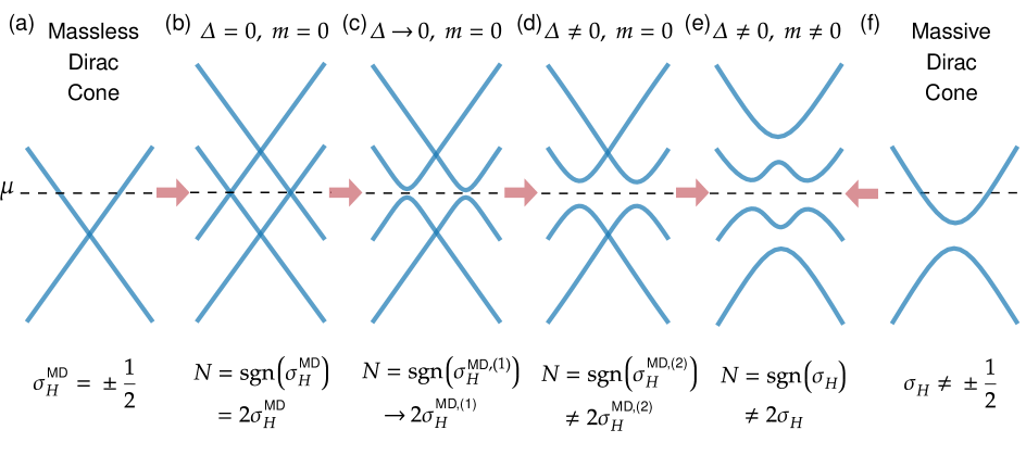
For a single Fermi loop, by allowing superconducting gap opened at the Fermi surface, and to perform the idealization, we first extract the relevant Dirac cone out of the rest of the bands without any coupling to the other bands, during which we further require no band gap closing and reopening. Then we can continuously deform the Dirac cone into a regulated massless/gapless Dirac cone, described by the Hamiltonian[65, 54]
| (A.1) |
where is the Dirac velocity, the mass term , (), and the pairing term is peaked at the Fermi surface.
The workflow is shown in Fig. 5. Start from leftmost (a), we require lies within the linear part, making the normal system carrying a half quantum Hall conductivity
| (A.2) |
where the sign depends on the chirality carried by the massless Dirac cone.
Moving one step right to (b), the Nambu space is introduced without superconducting gap, and (here not Chern number as the gap closing) follows as
| (A.3) |
This stands since is reduced by , since there is no particle-hole mixture, and .
One step further to (c), an infinitesimal superconducting gap is opened up near the Fermi surface. We can then cut the band structure into two parts, one low-energy part as a round centered at including the Fermi surface (and its neighboring states with non-zero pairing), and the other high-energy part correspondingly. Under the situation, the high-energy part of the band is indeed un-affected by the pairing, with particle-hole decoupled wavefunction for particle and for hole still, and time-reversal breaking non-zero mass term only appears in this part, which still leads to contribution to and as in normal band structure. The time-reversal unbroken low-energy part will develop a mixed wavefunction for occupied states, but is decoupled into direct product form of
| (A.4) |
with , the azimuthal angle of , and the polar angle in particle-hole space by , . This winding–particle-hole decoupled form will not contribute to either or . However, since the band structure is gapped, now shares the meaning of superconducting Chern number, and we write
| (A.5) |
with upper index indicating the change.
Another step right to (d), we now relax the pairing distribution to deform into its possible configuration (for instance, a uniform constant), with no band gap closing and reopening near Fermi level. Due to the topological protection by the superconducting gap, the Chern number remains unchanged, while the AHC is generally not half-quantized, since it is not a topological invariant in the superconducting state, and we write
| (A.6) |
with upper index indicating the second change of massless Dirac cone.
For the second last step (e), we let the Dirac cone acquire its low-energy mass to be a massive Dirac cone. As no band gap closing and reopening near Fermi level, the superconducting Chern number remains unchanged,
| (A.7) |
Thus we conclude that a superconducting gapped massive Dirac cone gives non-trivial . Finally, we embed the relative bands back to the original band structure, where the superconducting Chern number remains unchanged.
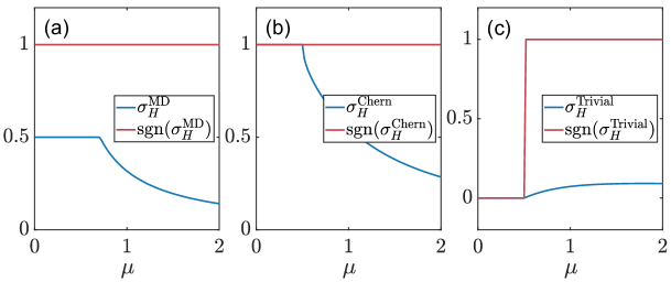
The sign of AHC represents the residual chirality of the band, a constant with the variation of the chemical potential as shown in Fig. 6, where we select massless, non-trivial massive, and trivial massive Dirac cones for illustration. When lies with a single Fermi loop, the sign of AHC is uniquely determined by , the property at the bottom of the band, not near the Fermi loop. Note for the massive case, when is in mass gap with no loop, the Hall conductance is quantized as an integer as dictated by TKNN theorem. Upon introducing superconductivity, the superconducting Chern number becomes twice the Hall conductance . The case when exceeds should be understood to evolve from an infinitesimal pairing at a single loop.
For the case of double Fermi loop, we employ the same strategy to extract and decouple the relative bands into two decoupled Dirac cones. Although this may superficially promote the symmetry of the system, only total superconducting Chern number summed from each superconducting gapped Dirac cones matters, and the value of each is not important. Then similarly, for the idealized paired massless Dirac cones, we have
| (A.8) |
with upper index for the Dirac cone index. Note that the inverse sign comes from the anomaly cancellation between the paired Dirac cones. We arrive at
| (A.9) |
After the back deformation, we have invariant Chern number, while the anomalous Hall conductance is generally not protected to be zero, as
| (A.10) |
This guideline can be generalized to multi-Fermi loop. By labelling Fermi loop in , the above procedure tells and generalizes the results to that
| (A.11) |
where is the Berry phase around -th Fermi loop defined using idealized massless Dirac cone, or equivalently the AHC by Stokes’s theorem. Note that here is protected by the emergent time-reversal or parity symmetry at Fermi surface in idealized band structure[64, 65, 54, 50, 66], and since it is defined on the boundary of 2D band-energy surface, no large gauge transformation is allowed. This formula is valid for both continuum and lattice models, and when they are consistent, the formula degrades to that in the main text
| (A.12) |
with the 1D winding number of the -th Fermi loop defined using idealized massless Dirac cone, with its contribution fixed by the sign of the AHC . Basically, a low-energy gives winding number . Also note that when extracting the relevant bands by decoupling, we can not change the Chern number carried by the rest of the bands. Meanwhile, there are cases with inseparable Fermi loops where they are assigned to the same band or bands with intersections. For the former, gauge consistency of occupied states need to be checked, while for the latter, one can perform idealization to isolate different bands without considering which parts of bands are connected, since we only care about the total Chern number.