SI.pdf
The impact of electrical contacts on the optical properties of a MoS2 monolayer
Abstract
Achieving high performance in transition-metal-dichalcogenide-based optoelectronic devices is challenging – the realization of an efficient electrical contacting scheme should not be obtained at the expense of their optical quality. Here we present the optical properties of MoS2 monolayers which have been electrically contacted with bismuth and gold. The photoluminescence (PL) spectrum of the samples contacted with both materials is significantly broadened. In the case of the bismuth contacted sample we note an additional, low energy band in the PL spectrum, attributed to a defect state formed during the evaporation of Bi. Comparing the intensity of the excitonic peak and of the defect-related peak, we note that there is a correlation between the type of contacts and the optical properties.
The unique electronic and optical properties of semiconducting van der Waals (vdW) materials make them attractive and promising candidates for optoelectronic devices [1, 2, 3, 4]. Among the most extensively studied two-dimensional (2D) materials are the transition metal dichalcogenides (TMDCs), in particular MoS2, MoSe2, WS2 and WSe2 [5, 6, 7]. These materials exhibit strongly bound excitons with high oscillator strength [8, 9], which led naturally to their study by means of various optical spectroscopic techniques. Excellent optical properties of these materials are also followed by interesting electrical properties, such as the valley Hall effect [10, 11].
An efficient contacting scheme is essential in order to fully exploit the optoelectronic potential of these materials and this has been proven to be challenging in the case of TMDCs [12, 13, 14]. Recent reports demonstrate the possibility of obtaining good ohmic contacts between a semimetallic material (bismuth or antimony) and a semiconducting TMDC layer [15, 16, 17]. Due to the near-zero density of states at the Fermi level of the semimetal, the formation of gap states in TMDCs, which are responsible for the Fermi-level pinning at the metal-TMDC interface, is sufficiently suppressed, making it possible to obtain low-resistance ohmic contacts to the TMDC. In order to fully exploit the potential of semimetal contacts to TMDCs, the exact physics at a semimetal/TMDC interface needs to be explored and understood [18]. However, combining optical and electrical investigations on the same sample is very challenging, due to the numerous processing steps needed for efficient contacting, which can lead to degradation of the optical quality of the sample [19]. Furthermore, the materials of choice for the fabrication of electrical contacts are usually not transparent to visible or infrared light [20, 21]. Finally, the optical properties of the sample can be influenced by the charge transfer through the contacts [22, 23].
In this work, we extend the approach of bismuth contacting by monitoring the emission response of MoS2/Bi heterostructures. We aim to investigate the influence of bismuth contacts on the optical properties of a MoS2 monolayer and to establish a correlation between the type and quality of the contacts and the optical properties of MoS2. With this goal in mind, we prepared a series of MoS2 monolayer samples with bismuth as the contact material. For all investigated samples we measured the electrical performance and the optical properties of the MoS2 flakes. Additionally, as a reference, we prepared and measured non-contacted and Au-contacted MoS2 flakes.
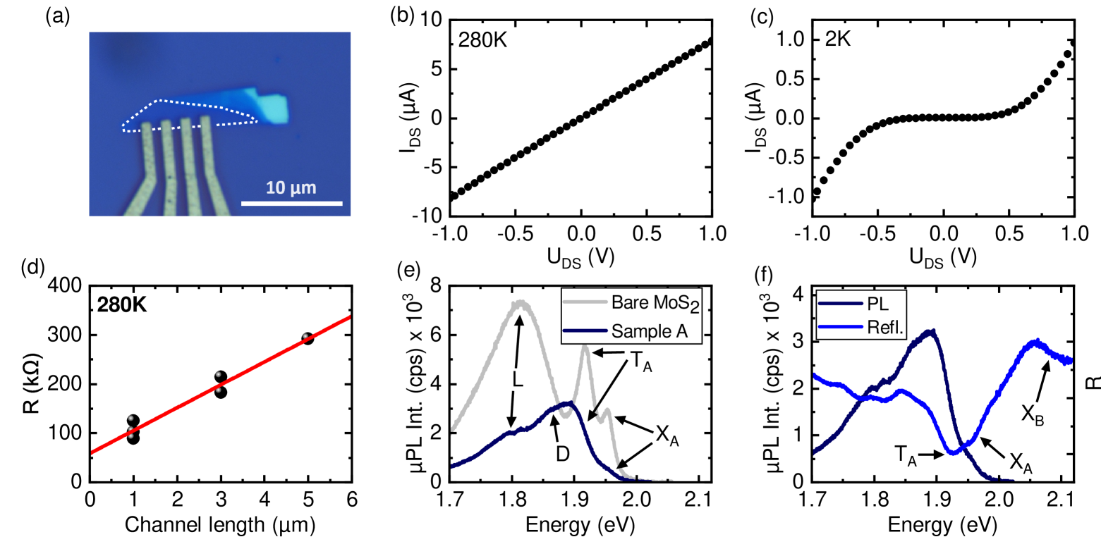
We first discuss the optoelectronic properties of the representative sample of the back-gated MoS2 monolayers with bismuth contacts, which we will refer to as sample A. We show its micrograph in Fig. 1(a). The layer was placed on a Si/SiO2 substrate, and bismuth contacts were evaporated in an ultra-high vacuum (UHV) system using an electron gun. We also prepared a series of reference samples with gold as a contact material. See the Supplementary Material for more details on the fabrication process.
We measured the current-voltage (I-V) curves of sample A for temperatures of . Fig. 1(b) shows the representative I-V curve for zero back-gate voltage at . The curve shows ohmic behavior, confirming that bismuth is a good contact material for MoS2 at room temperature [15, 16, 17]. The contacts lose their ohmic characteristics at temperatures below (see Fig. 1(c)), but they still conduct current. Fig. 1(d) presents the total resistance as a function of channel length (distance between contacts). We can observe the resistance increasing linearly with the channel length, which indicates that the total resistance is dominated by the resistance of the channel.
Sample A was optically investigated by measuring microreflectivity and microphotoluminescence (PL) spectra at . Fig. 1(e) shows a representative PL spectrum of sample A (dark blue line) and of the bare MoS2 monolayer exfoliated directly on the SiO2 substrate (gray line). The bare flake exhibits the typical low temperature PL spectrum of MoS2, with three distinct emission lines. We attribute the high energy peak at to the recombination of the neutral exciton (X), the peak at to the recombination of the charged exciton (T), while the low-energy broad band, labelled L in Fig. 1(e), is related to the recombination of excitons bound to defects present in the MoS2 monolayer [24, 25]. The higher intensity of the T line compared to that of the X line indicates charge doping, which in the case of MoS2 has an n-type character, as MoS2 is a naturally n-doped material [26]. This is consistent with the observation of n-type current in electrical measurements. The PL spectrum of sample A is significantly different from that of the bare flake. The total intensity of the observed emission is strongly quenched and the emission lines are not so well resolved anymore. The maximum of the emission is now at , i.e., at slightly lower energy than the T line. This is the result of a new, broad emission line appearing at , i.e., between the T and L lines, which we label D. To properly assign the observed emission lines to the corresponding optical transitions we performed reflectivity measurements on the investigated samples. In Fig. 1(f) we compare the PL spectrum of sample A with a reflectivity spectrum measured on another MoS2 monolayer sample with bismuth contacts. The transitions clearly visible in the reflectivity spectrum correspond to the charged exciton at , the A exciton at , and the B exciton at [5]. The presence of a trion-related resonance in the reflectivity spectrum suggests significant doping, which induces a partial transfer of the oscillator strength from the exciton to the charged exciton transition [27, 28]. All exciton transitions in reflectivity are in good agreement with the literature values [29]. However, there is no visible transition in the reflectivity at , which suggests that line D corresponds to the defect-related emission (discussed in the following).
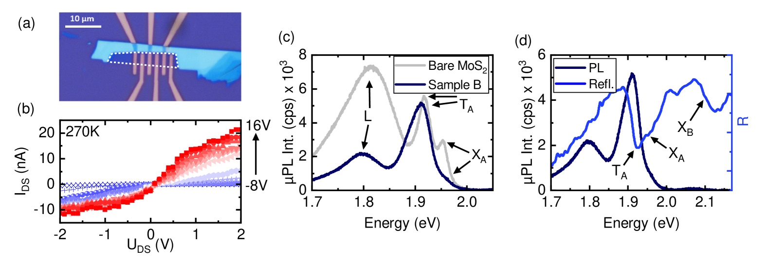
To check whether the D line is characteristic only for the Bi-contacted samples, we also prepared and measured a set of samples with Au contacts [30], and the optical microscope image of the representative Au-contacted sample (sample B) is presented in Fig. 2(a). Whereas more details on fabrication, processing, and results of optical and electrical measurements of these samples can be found in the Supplementary Material, here we present the most relevant features. In Fig. 2(b) we show the representative I-V curves measured at , showing Schottky-like characteristics. In Fig. 2(c) and (d) we show, respectively, a representative PL and reflectance spectra of sample B at . Similarly as for sample A, the PL lines are broadened compared to those for the bare MoS2, but there is no signature of any additional line close to the line. This leads us to the conclusion that the apparent additional line labelled D in Fig. 1 appears as a result of bringing the MoS2 flake into contact with Bi. In similar experiments performed on CVD-grown MoS2 monolayers covered with thin semimetal layers [31], Feng et al. observed red shift of the PL emission at room temperature. They explained it as a consequence of the transfer of electrons from Bi to MoS2, resulting in an increase in the electron concentration in MoS2 and an increase of the intensity of the T emission relative to the X emission. This transfer of electrons from Bi to MoS2 is not unexpected, as theoretical calculations show that at the Bi / MoS2 interfaces, electrons tend to accumulate at the S atoms due to their stronger electronegativity than for the Bi atoms [18, 31]. One cannot exclude possible diffusion of Bi atoms into MoS2, which would result in electron doping; however, there is not much information in the literature on doping of MoS2 with Bi [32]. Qumar et al. [33] observed a small redshift in PL from Bi-doped MoS2 nanosheets with Bi atoms; however, they did not explicitly state whether Bi substituted S or Mo atoms. The diffusion of Bi atoms into MoS2 would also be consistent with the fact that the D line appears on the entire surface of the sample, also on parts of the flake far from the contacts.
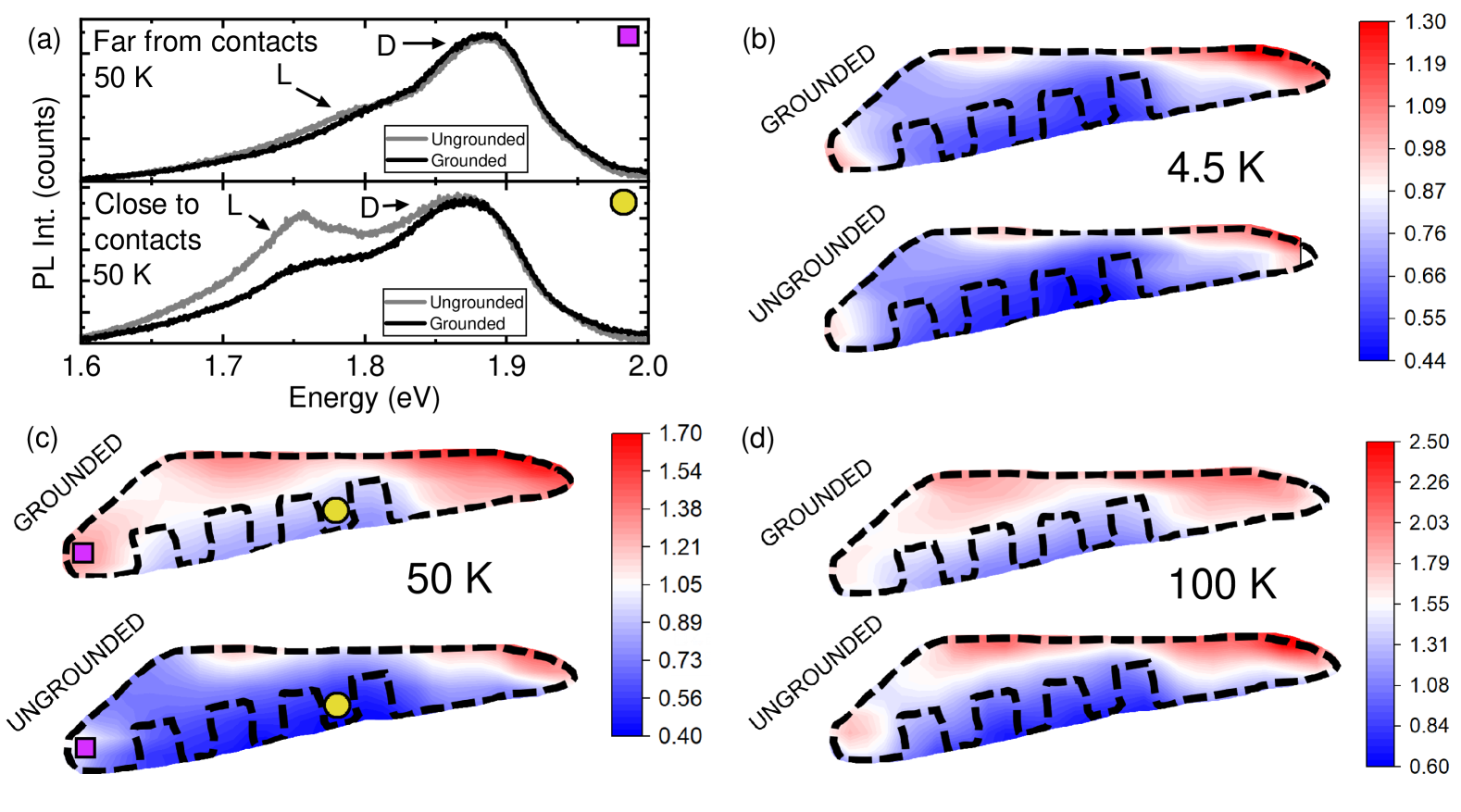
To check how the presence of excess free carriers in the flake affects the PL spectrum, we performed PL measurements at , , and with all electrical contacts grounded and not grounded, assuming that the grounding removes excess charge carriers. Generally, in case of sample A, there is a substantial difference in the optical spectrum when we ground the contacts or leave them ungrounded. Grounding leads to a decrease of the intensity of defect L and to negligible changes in the intensity of trion and D lines, as illustrated in Fig. 3 (a), where we plot the PL spectra of two spots on the sample - far from contacts (the violet square) and close to contacts (the yellow circle). We can observe the quench of defect L emission on both spots, but in case of the spot close to the contacts, this effect is more pronounced. Fig. 3(b)-(d) shows PL maps of the trion-to-defect ratio at selected temperatures for grounded and ungrounded contacts for sample A, where the intensity ratio was obtained by integration in the ranges corresponding to the trion at ( range width) and to the defect-bound excitons at ( range width), where the former range includes also the line D at . The ranges were red-shifted with the temperature, according to the temperature shift of the peaks. The ratio is clearly larger for grounded contacts, indicating that excess charge carriers transferred across the contacts bind mainly to the defects present in the crystal, while the trion and exciton emission lines are not significantly influenced. The effect is the strongest at . We relate this to the fact that at this temperature the contacts have much smaller resistance compared to the resistance at , which increases the possibility of charge transfer. In addition, at low temperatures, the carriers are tightly bound, which means they can not be freely transferred through the contacts. However, the defect emission is generally significantly suppressed at higher temperatures, which would make comparison with the trion intensity impossible. We can conclude that the charge transfer through the working contacts mostly affects the excess charge in the flake. As D emission is not significantly influenced by grounding, we can conclude that it is of a different nature than L.
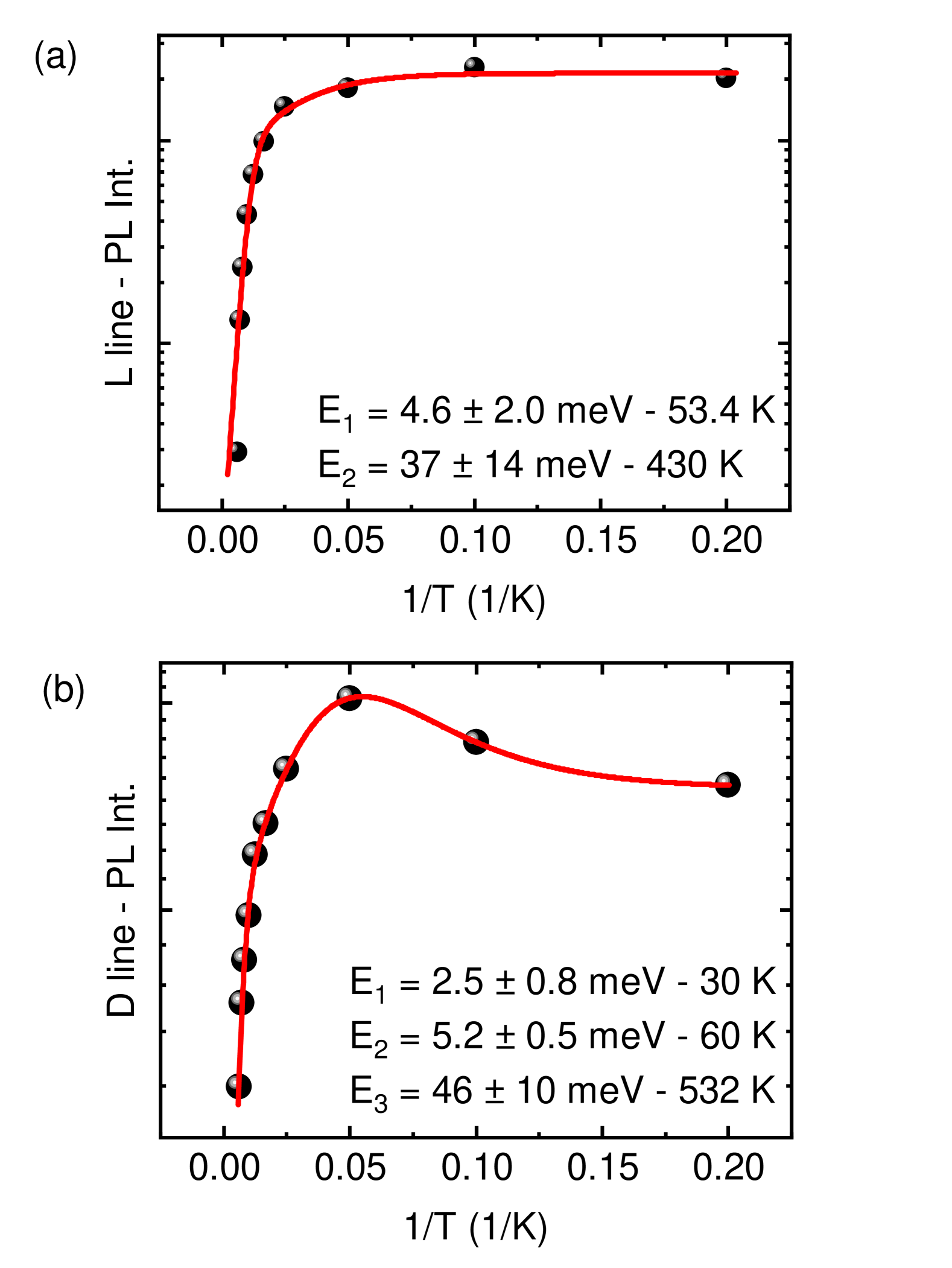
To analyze in more depth the effects described above, we measured the temperature dependence of the PL spectrum of sample A in the range of . We fitted the curves with four Gaussian peaks to obtain the emission intensity of the L and D lines as a function of temperature and fitted the Arrhenius plot of the obtained data to extract the activation energies of the relevant processes of exciton dissociation [34]. In case of line L we used the formula with two activation energies for PL quenching:
| (1) |
In case of peak D we used the formula with three activation energies - one for the increase of the PL at low temperatures and two for PL quenching at higher temperatures:
| (2) |
where is the activation energy and is the amplitude of the process. The results of the fitting are presented in Fig. 4. We compared the obtained values with the binding energies of various excitonic complexes on different types of defects in TMDCs, calculated with Monte Carlo simulations by Mostaani et al. [35]. In case of line L, the lower activation energy of is consistent, within the measurement error, with the dissociation, with the acceptor states possibly created by a carbon atom placed in a sulphur vacancy. This energy corresponds to a thermal energy at , which means that at the carriers are not tightly bound and some of them can escape through the potential barrier at the contacts. The higher energy of could indicate dissociation of a complex. In case of line D, the activation energy of for the initial increase in PL is also consistent with the dissociation of . This could mean that the carriers previously dissociated from the line L bind to the states responsible for D emission, although another, unknown reservoir of carriers could also be involved. The activation energy of the first quench process of line D, equal to , may be related to the dissociation of the or complex. This energy corresponds to the thermal energy at . The fact that despite that, the line D is not significantly influenced by grounding at could be explained by the supply of carriers from the above-mentioned reservoir with the activation energy of , which could replace the carrier that escape through the potential barrier at the contacts. The second quenching process, with an activation energy of , is consistent with the dissociation of a biexciton bound to an acceptor (), with a calculated . Therefore, if we assume the diffusion of Bi atoms during the evaporation process and formation of acceptor states as a result of sulphur substitution, we could explain the line D as originating from the emission of excitons and biexcitons bound to Bi acceptors. A more detailed analysis of the Arrhenius plots is presented in the Supplementary Material. There, we also show the trion-to-defect maps of sample B at with grounded and ungrounded contacts. There is no significant difference between the two maps, which probably results from the high resistance of the Schottky contacts at low temperatures.
In conclusion, we presented the properties of MoS2 monolayers, which have been electrically contacted with semimetallic bismuth. The contacts show ohmic behavior in the temperature range from to , whereas the gold contacts used as a reference exhibit Schottky characteristics throughout the entire range. The two materials used to fabricate the contacts also significantly affect the optical properties of the MoS2 monolayers. In the case of the bismuth contacts, an additional defect band in the PL spectrum is attributed to the diffusion of bismuth atoms during the deposition process.
Finally, by comparing the PL spectra of grounded and ungrounded samples at , we demonstrate that the grounded bismuth contacts significantly reduce the intensity of defect-bound excitons, which we attribute to charge transfer through the grounded contacts removing the charges bound to defects. This effect is not observed in the sample with gold contacts, which is associated with their Schottky-like characteristics. Overall, our results show that bismuth contacts are very strong candidates for electrical contacting in high quality, TMD-based optoelectronic devices. However, their effect on the optical spectrum of TMDC requires further exploration.
See the Supplementary Material for details on the processing of the samples, measurements details, and additional results.
This work was financially supported from the project no. 2022/45/B/ST5/04292, funded by the National Science Centre in Poland. We also acknowledge financial support from the European Union (EU) student exchange programme Erasmus+ Internship.
Author declaration
Conflict of Interest
The authors have no conflicts to disclose.
Author Contributions
Agata Zielińska: Data Curation (lead); Formal Analysis (lead); Writing - Original Draft Preparation (lead). Mateusz Dyksik: Conceptualization (equal); Methodology (equal); Supervision (supporting); Validation (equal); Writing - Original Draft Preparation (supporting). Alessandro Surrente: Validation (equal); Writing - Original Draft Preparation (supporting). Jonathan Eroms: Resources (equal); Supervision (supporting); Writing - Review and Editing (equal). Dieter Weiss: Resources (equal); Writing - Review and Editing (equal). Paulina Płochocka: Project Administration (supporting); Resources (equal); Validation (equal); Writing - Review and Editing (equal). Mariusz Ciorga: Conceptualization (equal); Funding Acquisition (lead); Methodology (equal); Project Administration (lead); Resources (equal); Supervision (lead); Validation (equal); Writing - Original Draft Preparation (supporting).
Data availability
The data that support the findings of this study are available from the corresponding author upon reasonable request.
References
- Liu et al. [2019] Y. Liu, Y. Gao, S. Zhang, J. He, J. Yu, and Z. Liu, Valleytronics in transition metal dichalcogenides materials, Nano Research 12, 2695 (2019).
- Avsar et al. [2020] A. Avsar, H. Ochoa, F. Guinea, B. Özyilmaz, B. J. van Wees, and I. J. Vera-Marun, Colloquium: Spintronics in graphene and other two-dimensional materials, Rev. Mod. Phys. 92, 021003 (2020).
- Mueller and Malic [2018] T. Mueller and E. Malic, Exciton physics and device application of two-dimensional transition metal dichalcogenide semiconductors, npj 2D Mater Appl 2, 1 (2018), publisher: Nature Publishing Group.
- Zollner et al. [2019] K. Zollner, P. E. Faria Junior, and J. Fabian, Proximity exchange effects in and heterostructures with : Twist angle, layer, and gate dependence, Phys. Rev. B 100, 085128 (2019).
- Wang [2013] Z. M. Wang, MoS2 (Springer Cham, 2013).
- Kolobov and Tominaga [2016] A. V. Kolobov and J. Tominaga, Two-Dimensional Transition-Metal Dichalcogenides (Springer, 2016).
- Wee et al. [2019] A. T. Wee, D. Chi, and K. Goh, 2D Semiconductor Materials and Devices (Elsevier Science, 2019).
- Chernikov et al. [2014] A. Chernikov, T. C. Berkelbach, H. M. Hill, A. Rigosi, Y. Li, B. Aslan, D. R. Reichman, M. S. Hybertsen, and T. F. Heinz, Exciton Binding Energy and Nonhydrogenic Rydberg Series in Monolayer , Phys. Rev. Lett. 113, 076802 (2014).
- Back et al. [2018] P. Back, S. Zeytinoglu, A. Ijaz, M. Kroner, and A. Imamoğlu, Realization of an Electrically Tunable Narrow-Bandwidth Atomically Thin Mirror Using Monolayer , Phys. Rev. Lett. 120, 037401 (2018).
- Mak et al. [2014] K. F. Mak, K. L. McGill, J. Park, and P. L. McEuen, The valley Hall effect in MoS2 transistors, Science 344, 1489 (2014).
- Habe and Koshino [2017] T. Habe and M. Koshino, Anomalous Hall effect in -phase transition-metal dichalcogenide monolayers on ferromagnetic substrates ( = Mo, W, and = S, Se, Te), Phys. Rev. B 96, 085411 (2017).
- Schulman et al. [2018] D. S. Schulman, A. J. Arnold, and S. Das, Contact engineering for 2D materials and devices, Chemical Society Reviews 47, 3037 (2018).
- Allain et al. [2015] A. Allain, J. Kang, K. Banerjee, and A. Kis, Electrical contacts to two-dimensional semiconductors, Nature Materials 14, 1195 (2015).
- Zheng et al. [2021] Y. Zheng, J. Gao, C. Han, and W. Chen, Ohmic Contact Engineering for Two-Dimensional Materials, Cell Reports Physical Science 2, 100298 (2021).
- Shen et al. [2021] P.-C. Shen, C. Su, Y. Lin, A.-S. Chou, C.-C. Cheng, J.-H. Park, M.-H. Chiu, A.-Y. Lu, H.-L. Tang, M. M. Tavakoli, G. Pitner, X. Ji, Z. Cai, N. Mao, J. Wang, V. Tung, J. Li, J. Bokor, A. Zettl, C.-I. Wu, T. Palacios, L.-J. Li, and J. Kong, Ultralow contact resistance between semimetal and monolayer semiconductors, Nature 593, 211 (2021).
- Li et al. [2023] W. Li, X. Gong, Z. Yu, L. Ma, W. Sun, S. Gao, C. Köroğlu, W. Wang, L. Liu, T. Li, H. Ning, D. Fan, Y. Xu, X. Tu, T. Xu, L. Sun, W. Wang, J. Lu, Z. Ni, J. Li, X. Duan, P. Wang, Y. Nie, H. Qiu, Y. Shi, E. Pop, J. Wang, and X. Wang, Approaching the quantum limit in two-dimensional semiconductor contacts, Nature 613, 274 (2023), publisher: Nature Publishing Group.
- Lee et al. [2024] S. Lee, X. Wang, H. Shin, N. Ali, T. D. Ngo, E. Hwang, G.-H. Kim, G. Y. Yeom, K. Watanabe, T. Taniguchi, and W. J. Yoo, Semi-Metal Edge Contact for Barrier-Free Carrier Transport in MoS2 Field Effect Transistors, ACS Applied Electronic Materials 6, 4149 (2024).
- Su et al. [2023] T. Su, Y. Li, Q. Wang, W. Zhao, L. Cao, and Y. S. Ang, Semimetal contacts to monolayer semiconductor: weak metalization as an effective mechanism to Schottky barrier lowering, Journal of Physics D: Applied Physics 56 (2023).
- Turunen et al. [2023] M. Turunen, H. Fernandez, S.-T. Akkanen, H. Seppänen, and Z. Sun, Effects of atomic layer deposition on the optical properties of two-dimensional transition metal dichalcogenide monolayers, 2D Materials 10, 045018 (2023).
- Fan et al. [2018] Y. Fan, C. Guo, Z. Zhu, W. Xu, F. Wu, X. Yuan, and S. Qin, Monolayer-graphene-based broadband and wide-angle perfect absorption structures in the near infrared, Scientific Reports 8 (2018).
- Johnson and Christy [1972] P. B. Johnson and R. W. Christy, Optical Constants of the Noble Metals, Phys. Rev. B 6, 4370 (1972).
- Ahmed et al. [2020] T. Ahmed, K. Roy, S. Kakkar, A. Pradhan, and A. Ghosh, Interplay of charge transfer and disorder in optoelectronic response in Graphene/hBN/MoS2 van der Waals heterostructures, 2D Materials 7, 025043 (2020).
- Grzeszczyk et al. [2020] M. Grzeszczyk, M. R. Molas, K. Nogajewski, M. Bartoš, A. Bogucki, C. Faugeras, P. Kossacki, A. Babiński, and M. Potemski, The effect of metallic substrates on the optical properties of monolayer MoSe2, Scientific Reports 10 (2020).
- Jadczak et al. [2017] J. Jadczak, J. Kutrowska-Girzycka, P. Kapuściński, Y. S. Huang, A. Wójs, and L. Bryja, Probing of free and localized excitons and trions in atomically thin WSe2, WS2, MoSe2 and MoS2 in photoluminescence and reflectivity experiments, Nanotechnology 28, 395702 (2017).
- Munson et al. [2024] K. T. Munson, R. Torsi, S. Mathela, M. A. Feidler, Y.-C. Lin, J. A. Robinson, and J. B. Asbury, Influence of Substrate-Induced Charge Doping on Defect-Related Excitonic Emission in Monolayer MoS2, The Journal of Physical Chemistry Letters 15, 7850 (2024).
- Park et al. [2023] Y. Park, N. Li, D. Jung, L. T. Singh, J. Baik, E. Lee, D. Oh, Y. D. Kim, J. Y. Lee, J. Woo, S. Park, H. Kim, G. Lee, G. Lee, and C.-C. Hwang, Unveiling the origin of n-type doping of natural MoS2: carbon, npj 2D Materials and Applications 7 (2023).
- Courtade et al. [2017] E. Courtade, M. Semina, M. Manca, M. M. Glazov, C. Robert, F. Cadiz, G. Wang, T. Taniguchi, K. Watanabe, M. Pierre, W. Escoffier, E. L. Ivchenko, P. Renucci, X. Marie, T. Amand, and B. Urbaszek, Charged excitons in monolayer : Experiment and theory, Phys. Rev. B 96, 085302 (2017).
- Sidler et al. [2017] M. Sidler, P. Back, O. Cotlet, A. Srivastava, T. Fink, M. Kroner, E. Demler, and A. Imamoglu, Fermi polaron-polaritons in charge-tunable atomically thin semiconductors, Nature Physics 13, 255 (2017).
- Tran et al. [2016] M. D. Tran, J.-H. Kim, and Y. H. Lee, Tailoring photoluminescence of monolayer transition metal dichalcogenides, Current Applied Physics 16, 1159 (2016).
- Zielińska et al. [2025] A. Zielińska, J. Prażmowska-Czajka, M. Dyksik, J. Eroms, D. Weiss, R. Paszkiewicz, and M. Ciorga, Study of gold and bismuth electrical contacts to a MoS2 monolayer, Solid State Communications 397, 115824 (2025).
- Feng et al. [2024] X. Feng, Z. G. Yu, H. Guo, Y. Li, Y.-W. Zhang, and K.-W. Ang, Direct Observation of Semimetal Contact Induced Charge Doping and Strain Effect in CVD-Grown Monolayer MoS2 Transistors, Advanced Electronic Materials 10, 2300820 (2024), _eprint: https://onlinelibrary.wiley.com/doi/pdf/10.1002/aelm.202300820.
- Sovizi and Szoszkiewicz [2022] S. Sovizi and R. Szoszkiewicz, Single atom doping in 2D layered MoS2 from a periodic table perspective, Surface Science Reports 77, 100567 (2022).
- Qumar et al. [2020] U. Qumar, M. Ikram, M. Imran, A. Haider, A. Ul-Hamid, J. Haider, K. Riaz, and S. Ali, Synergistic effect of Bi-doped exfoliated MoS2 nanosheets on their bactericidal and dye degradation potential, Dalton Transactions 49, 5362 (2020).
- Shibata [1998] H. Shibata, Negative thermal quenching curves in photoluminescence of solids, Japanese Journal of Applied Physics 37, 550 (1998).
- Mostaani et al. [2017] E. Mostaani, M. Szyniszewski, C. H. Price, R. Maezono, M. Danovich, R. J. Hunt, N. D. Drummond, and V. I. Fal’ko, Diffusion quantum monte carlo study of excitonic complexes in two-dimensional transition-metal dichalcogenides, Phys. Rev. B 96, 075431 (2017).