Electric field tunable spin-orbit gap in a bilayer graphene/WSe2 quantum dot
Abstract
We report on the investigation of proximity-induced spin-orbit coupling (SOC) in a heterostructure of bilayer graphene (BLG) and tungsten diselenide (WSe2). A BLG quantum dot (QD) in the few-particle regime acts as a sensitive probe for induced SOC. Finite bias and magnetotransport spectroscopy measurements reveal a significantly enhanced SOC that decreases with the applied displacement field, distinguishing it from pristine BLG. We attribute this tunability to an increased layer localization of the QD states on the BLG layer distant to the WSe2. Furthermore, our measurements demonstrate a reduced valley -factor at larger displacement fields, consistent with a weaker lateral confinement of the QD. Our findings show evidence of the influence of WSe2 across BLG layers, driven by reduced real-space confinement and increased layer localization at higher displacement fields. This study demonstrates the electrostatic tunability of spin-orbit gap in BLG/WSe2 heterostructures, which is especially relevant for the field of spintronics and future spin qubit control in BLG QDs.
I Introduction
Bernal stacked bilayer graphene (BLG) is characterized by its low intrinsic spin-orbit coupling (SOC). Theory predicts a Kane-Mele type SOC strength of about 24 eV [1] whereas experiments have revealed values in a range of 50-80 eV [2, 3, 4, 5, 6], mainly considered to be enhanced due to proximity coupling to hBN. The integration of transition metal dichalcogenides (TMDs) in graphene-based heterostructures has enabled an interesting approach for manipulating the SOC in two-dimensional materials. For example, coupling graphene to a TMD, such as tungsten diselenide (WSe2), has shown promising potential to enhance the intrinsically low SOC in graphene while preserving its exceptionally high carrier mobility [7, 8, 9, 10, 11, 12, 13, 14]. Of particular interest are BLG/TMDs heterostructures, thanks to the possibility of tuning the band structure of BLG with an external out-of-plane electric displacement field (-field), which introduces a gate-tunable band-gap [15, 16, 17] and localize the charge carriers predominately on one of the graphene layers [18, 19, 20]. Since only the graphene layer in direct contact to the TMD is expected to exhibit significant proximity-induced SOC, this results in a splitting of either the conduction or valence band depending on the sign, i.e. direction of the -field [19, 20]. Furthermore, BLG/WSe2 heterostructures demonstrate high electronic quality with charge carrier mobilities exceeding cm2(Vs)-1 allowing for ballistic transport [12, 21] and large spin diffusion lengths [22, 23, 24], making it suitable for the development of spin transistors [25, 26]. This unique combination of high carrier mobility, gate-tunable SOC, and spin-dependent electronic band properties makes BLG/TMD heterostructures a versatile platform for spintronics applications, with implications for the design of next-generation spin-based transistors and quantum devices.
Until now, proximity-induced SOC has been investigated predominantly in bulk-like BLG/WSe2 devices, where the nearly perfect layer localization at low energies keeps band mixing to a minimum. However, when lateral confinement is introduced, as in gate defined QDs in BLG, the wavefunction can significantly mix multiple bands and layers, leading to more pronounced band mixing and modified SOC behavior. Here, we investigate the proximity effect of WSe2 on the SOC in a BLG hole QD, where the QD wavefunction predominantly occupies the graphene layer opposite to the WSe2 layer. By magnetotransport and finite-bias spectroscopy measurements in the single charge-carrier regime, we show that the spin-orbit gap in the BLG-QD exhibit a pronounced dependence on the displacement field , increasing at lower -fields, while the spin -factor remains largely unchanged. Additionally, we find that the valley -factor decreases for larger displacement fields, indicating a lateral size increase of the QD. We attribute this trend to the interplay of enhanced layer localization in the BLG conduction and valence bands and a reduction in lateral confinement at increased displacement fields.
II Device fabrication and operation
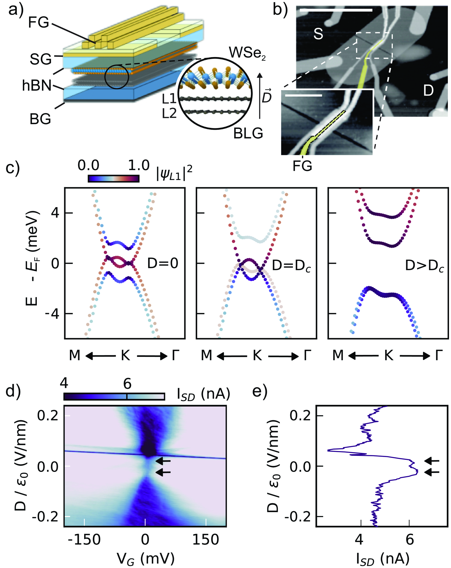
The device consists of a monolayer of WSe2 on top of a BLG flake, both encapsulated between two approximately 40 nm thick crystals of hexagonal boron nitride (hBN). This van der Waals heterostructure is placed on top of a graphite flake that functions as a back gate (BG). Three metal (Cr/Au) gate layers – split gates (SGs) and two layers of interdigitated finger gates (FGs), – are deposited on top of the heterostructure, each separated by a 20 nm thick layer of Al2O3. Fig. 1(a) shows a schematic of the heterostructure, whereas Fig. 1(b) shows a scanning force microscope image of the gate structure. All the experiments were performed in a dilution refrigerator at a base temperature of around 30 mK.
The SGs are used to open a band gap in the BLG beaneth them, creating a narrow ( 200 nm wide) conducting channel connecting the source (S) and drain (D) contacts. The voltages applied to the BG and SGs allow to independently tune the effective gate voltage, , and the displacement field, , where is the ratio between the geometric lever arms of the BG and the SGs respectively, while and are the offset voltages of the charge neutrality point [17]. Figure 1(d) shows the source-drain current as a function of and . The data shows a non-monotonic dependency of the current near the charge neutrality point at low displacement fields. A cut through the current map at V reveals a local minimum in at mV/nm and two symmetrically centered local maxima at the critical field (indicated by the black arrows in Figs. 1(d) and (e)). Similar features as in Fig. 1(d) have been observed in conductance measurements of dual gated suspended BLG devices, which was attributed to a symmetry broken state due to electron-electron interaction [29]. Recently, this inverted gap phase was also observed in transport measurements of BLG fully encapsulated between WSe2 [30], as well as in samples with an one-sided contact to TMDs, such as WSe2 [27] and MoS2 [28]. In this case, the feature is attributed to band inversion caused by induced Ising-type SOC. Indeed, tight-binding band-structure calculations indicate the existence of a critical field for which the SOC-induced gap closes, see Fig. 1(c). At this critical field, the band gap closes showing up as peaks in the current (c.f. Fig. 1(e)), while the breaking of layer symmetry leads to a dip in current at V/nm. The signature of this inverted gap phase is less pronounced in our data, due to our signal being dominated by the induced conductive channel in the device, which is only gated by the BG. Nevertheless, this is a clear evidence of an enhanced proximity-induces spin-orbit coupling in the BLG.
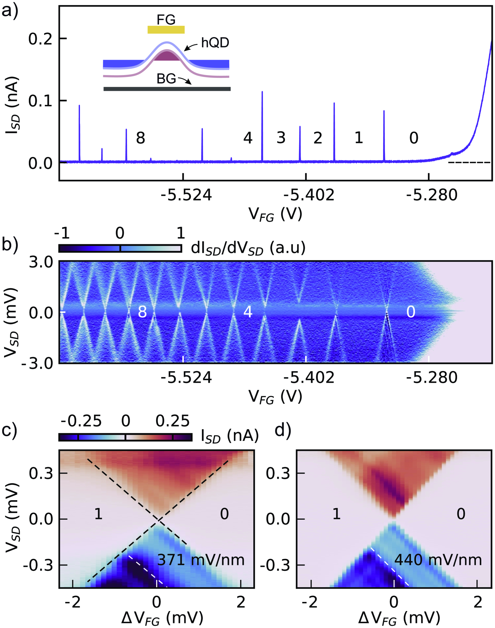
The finger-gate structure on top of the split-gate allows us to modulate the potential profile along the conducting channel and to form a quantum dot, see inset in Fig. 2(a) [31, 32, 33]. We deplete the channel form an electrostatically defined QD in BLG, by applying a voltage to the central finger gate, while the remaining FGs are used to tune the tunnel barriers and isolate the QD. Figure 2(a) shows the complete pinch-off of the current through the channel for increasing , and the appearance of well-defined Coulomb peaks indicating the sequential filling of a QD with holes. Figure 2(b) shows a finite-bias spectroscopy measurement, i.e. the normalized differential conductance as a function of and the bias voltage . From the characteristic Coulomb diamond signature, we extract the gate lever arm , which allows us to translate changes in gate voltage into a changes in electrochemical potential .
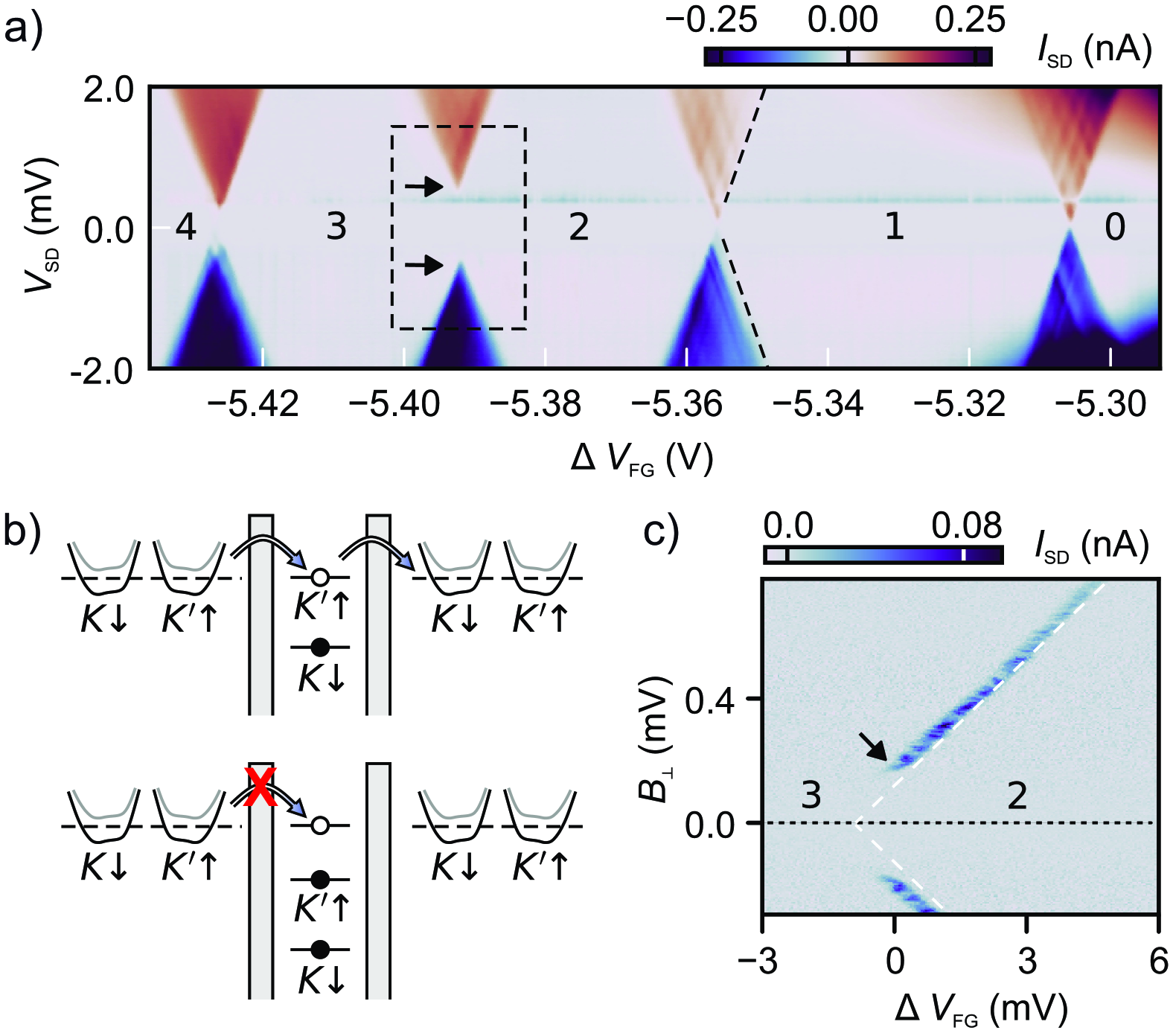
The Coulomb-blockade measurements bring also signatures of the presence of proximity-induced SOC gap into the BLG. Indeed we observe that the third Coulomb diamond is not properly closing (see dashed box in Fig. 3(a)). This can be understood in terms of an imbalance of the four flavors (, , and ) in the lead regions, which for large displacement field, have a band-structure with spin split bands as shown as in the right panel if Fig. 1c. Due to this imbalance, the first two holes, and can be easily filled and low-bias transport is possible (see upper schematic of Fig. 3(b)). However, the process of adding the hole, which corresponds to a or state, is suppressed (see lower schematic). The imbalance can be either lifted by the bias voltage (see arrows in Fig. 3(a)) or by out-of-plane -field (see Fig. 3(c)). These processes make it possible to populate or states in the leads or to change the three particle ground-state making transport possible.
Finite-bias spectroscopy measurements also allow to investigate the excited states of the QD [34], as shown in Figs. 2(c) and (d) for two different displacement field. This type of measurements allow to determine the single-particle level splitting. In our case, the first excited state is expected to coincide with the SO-gap, since orbital excited states are expected to be split by eV. As discussed below, the values extracted for the first excited state agrees very well with the SOC strength estimated by magnetic field spectroscopy. The data of Fig. 2c present therefore a first indication that the SOC in the dot depends on the applied displacement field.
III Magnetic field spectroscopy
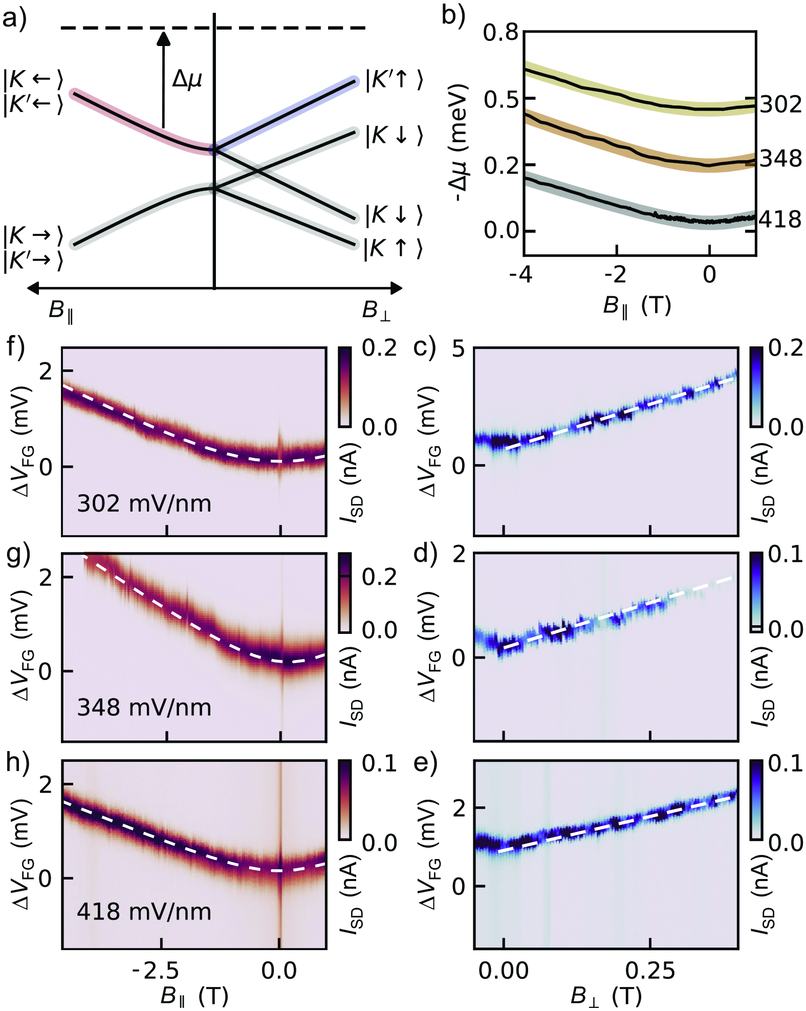
The size of the SOC gap in the dot, , and the values of the spin and valley -factors, and can be experimentally determined by measuring the shift of the first Coulomb resonance as function of an external magnetic field, since this reflect directly the change of the ground-state energy of the single particle states, see Fig. 4(a). This exhibits a linear dependence on the out-of-plane magnetic field given by the relation
| (1) |
and the following dependence on the in-plane field :
| (2) |
where is the Bohr magneton, the spin -factor, is the valley -factor, originating from the orbital valley magnetic moment caused by a non-vanishing Berry curvature at the high symmetry points and [35], and is the spin-orbit gap. The shift of the first Coulomb resonance as function of and are shown in Figs. 4(c)-4(h) for different values of the applied displacement field . Knowing the gate lever-arm from the finite-bias spectroscopy measurements, it is possible to translate the shift of the resonance in gate-voltage into a change of electrochemical potential , as shown in Fig. 4(b) for the measurements as function of .
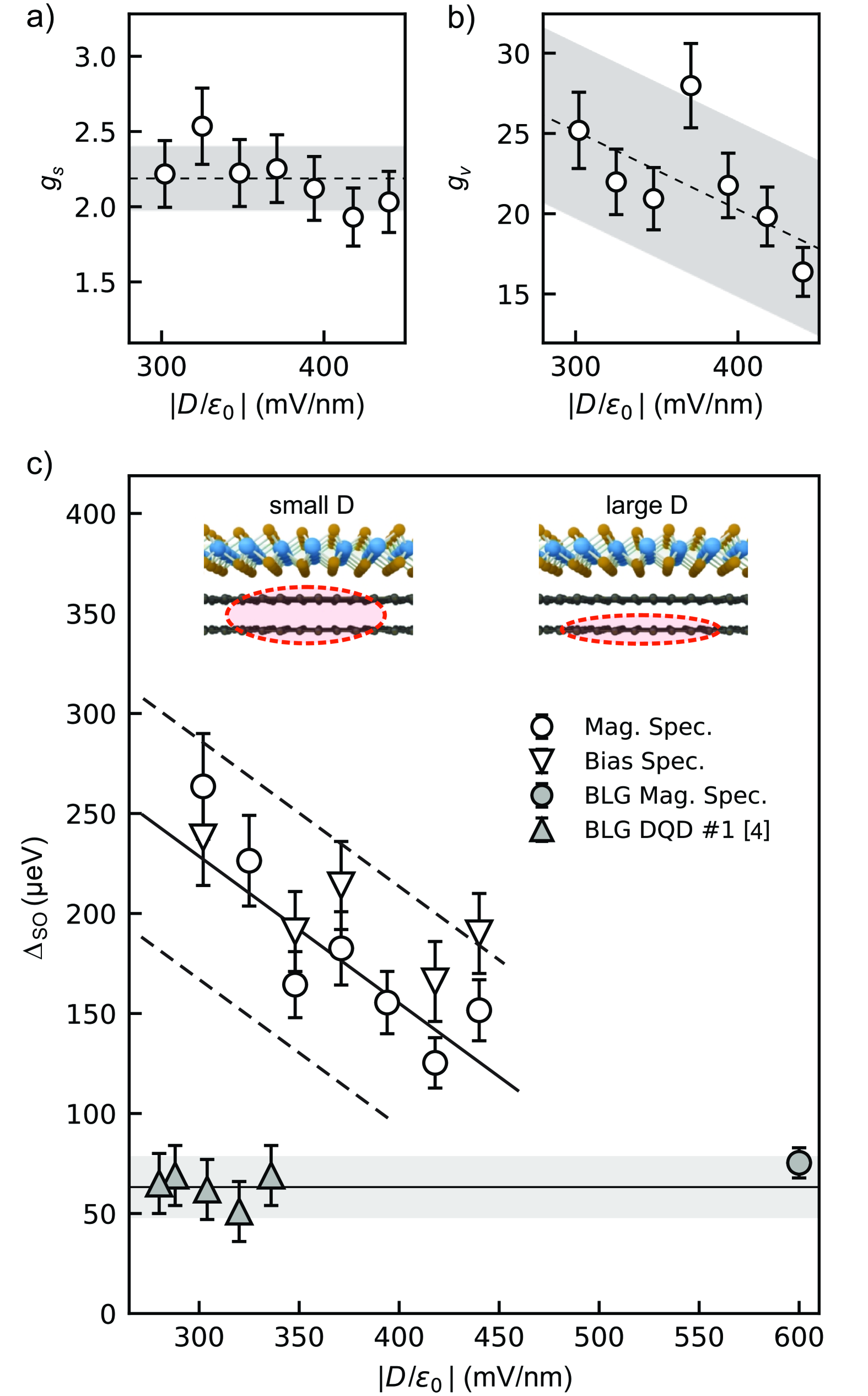
At large magnetic field, the peak position shift approximately linearly with , , which allows to extract the spin -factor independently. As expected, the values of extracted in this way show no dependence on within the margin of error, see Fig. 5(a). The main source of uncertainty in this process is the value of the lever-arm, which we estimate to have a systematic error of . Taking the mean value of determined in this way as fixed parameter, , we fit Eq. (1) and Eq. (2) to the data of Fig. 4, to determine and respectively. The values determined in this way are summarized in Fig. 5. In Fig. 5(c) we include also values of determined with finite bias spectroscopy (down-pointing white triangles), which agree very well with those extracted with the procedure discussed above.
Differently from the spin -factor, both the valley -factor, , and the spin-orbit coupling show a clear dependence on the applied displacement field, both decreasing with increasing . The decrease of indicates a weaker lateral confinement for larger , in agreement with earlier work [36]. This weaker lateral confinement is also one of the effects that leads to the observed reduction of for increasing , as discussed in the following section.
IV Tunable proximity-induced spin-orbit gap
At low displacement field, the extracted SOC strength is significantly larger than what was observed in QDs formed in pure BLG-hBN heterostructures [4, 37], see also gray data-points in Fig. 5(c)). Such an enhancement is a clear indication of proximity-induced SOC caused by the WSe2 layer in our heterostructure. Interestingly, our QD is expected to be located on the BLG layer opposite from the WSe2. In fact, in gapped BLG, the valence and conduction bands near the - and -valleys are layer-polarized: one layer predominantly hosts the conduction band, while the other hosts the valence band. The polarity of the displacement field determines which band localizes on the top (WSe2-side) or bottom graphene layer [19, 20]. In our device, the conduction band is localized on the top-layer, which implies that for negative doping, we fill states in the valence band localized on the bottom graphene layer. To form a QD in the hole regime, the charge-carrier polarity must be locally inverted, so the QD wavefunction predominantly derives from bottom-layer states. Despite this nominal separation, the measurements reveal a substantial proximity-induced SOC effect.
One reason for this is that the layer localization is most pronounced right at the and -points, while away from these high-symmetry points, the Bloch wavefunctions experience increased mixing across both layers, providing overlap with the top graphene layer. In the quantum dot, the real-space confinement of the wavefunction results in momentum-space mixing of Bloch states, enhancing the contribution from the proximitized BLG layer and resulting in the observed enhanced . However, for increasing the displacement field, the layer-polarization (i.e. layer localization) of the wavefunction increases (see schematics in Fig. 5(c)) and, at the same time, the lateral confinement of the dot is reduced [36], as indicated by decreasing values of the valley -factor, see Fig. 5(b), narrowing the distribution of the wave function in momentum space around layer-polarized states. The two effects contributes to the observed decrease of with increasing .
V Conclusion
In summary, we have experimentally investigated the proximity-induced SOC in a BLG QD formed adjacent to a WSe2 layer. Through magnetotransport and finite bias spectroscopy measurements in the few-carrier regime, we find a pronounced enhancement of the SOC gap compared to well studied pure BLG QDs, underscoring the impact of the TMD on nearby graphene layers. This spin-orbit gap decreases with increasing , which is in contrast to pristine BLG QDs, where no tuning of with was observed. This behavior can be understood as the interplay of two key effects: (i) a larger band gap strengthens layer localization at the high-symmetry points , and (ii) the lateral confinement of the QD decreases at higher , causing the wavefunction to include fewer mixed-layer states that would otherwise enhance the SOC strength.
Notably, we observe that the QD primarily resides on the graphene layer opposite to the WSe2, yet still exhibits a sizeable proximity-induced SOC.
This highlights the importance of momentum-space mixing of Bloch states and shows that a purely layer-localized picture is insufficient at experimentally relevant gate voltages and QD sizes.
Furthermore, our out-of-plane magnetotransport data reveal a systematic reduction of the valley -factor with increasing , consistent with reduced lateral confinement and a larger real-space extent of the QD.
Altogether, these findings demonstrate robust, tunable SOC in a BLG/WSe2 heterostructure, paving the way for future spintronic and QD-based spin qubit experiments where electrical control of spin-orbit coupling may be used to spin-orbit driven qubits and spin-based logic devices.
While finalizing the manuscript we became aware of another recent work studying a BLG QD in proximity to a WSe2 layer [38]. Interestingly, their observed dependency of the proximity enhanced spin orbit gap on is in very good qualitative and quantitative agreement supporting our findings.
Acknowledgements
The authors thank F. Lentz, S. Trellenkamp and M. Otto for help with sample fabrication and F. Haupt for help on the manuscript.
This project has received funding from the European Research Council (ERC) under grant agreement No. 820254, the Deutsche Forschungsgemeinschaft (DFG, German Research Foundation) under Germany’s Excellence Strategy - Cluster of Excellence Matter and Light for Quantum Computing (ML4Q) EXC 2004/1 - 390534769, and by the Helmholtz Nano Facility [39].
K.W. and T.T. acknowledge support from the JSPS KAKENHI (Grant Numbers 21H05233 and 23H02052) and World Premier International Research Center Initiative (WPI), MEXT, Japan.
Author contributions
H.D, D.E. and E.I. fabricated the device. H.D. and D.E. performed the measurements and analyzed the data with the help of L.M. and S.M. K.W. and T.T. synthesized the hBN crystals. C.V. and C.S. supervised the project. H.D., D.E., K.H., C.V., and C.S. wrote the manuscript with contributions from all authors.
Competing interests The authors declare no competing interests.
References
- Konschuh et al. [2012] S. Konschuh, M. Gmitra, D. Kochan, and J. Fabian, Theory of spin-orbit coupling in bilayer graphene, Phys. Rev. B 85, 115423 (2012).
- Sichau et al. [2019] J. Sichau, M. Prada, T. Anlauf, T. J. Lyon, B. Bosnjak, L. Tiemann, and R. H. Blick, Resonance Microwave Measurements of an Intrinsic Spin-Orbit Coupling Gap in Graphene: A Possible Indication of a Topological State, Phys. Rev. Lett. 122, 046403 (2019).
- Banszerus et al. [2020a] L. Banszerus, B. Frohn, T. Fabian, S. Somanchi, A. Epping, M. Müller, D. Neumaier, K. Watanabe, T. Taniguchi, F. Libisch, B. Beschoten, F. Hassler, and C. Stampfer, Observation of the Spin-Orbit Gap in Bilayer Graphene by One-Dimensional Ballistic Transport, Phys. Rev. Lett. 124, 177701 (2020a).
- Banszerus et al. [2021] L. Banszerus, S. Möller, C. Steiner, E. Icking, S. Trellenkamp, F. Lentz, K. Watanabe, T. Taniguchi, C. Volk, and C. Stampfer, Spin-valley coupling in single-electron bilayer graphene quantum dots, Nat. Commun. 12, 5250 (2021).
- Kurzmann et al. [2021] A. Kurzmann, Y. Kleeorin, C. Tong, R. Garreis, A. Knothe, M. Eich, C. Mittag, C. Gold, F. K. de Vries, K. Watanabe, T. Taniguchi, V. Fal’ko, Y. Meir, T. Ihn, and K. Ensslin, Kondo effect and spin–orbit coupling in graphene quantum dots, Nat. Commun. 12, 6004 (2021).
- Duprez et al. [2024] H. Duprez, S. Cances, A. Omahen, M. Masseroni, M. J. Ruckriegel, C. Adam, C. Tong, R. Garreis, J. D. Gerber, W. Huang, L. Gächter, K. Watanabe, T. Taniguchi, T. Ihn, and K. Ensslin, Spin-valley locked excited states spectroscopy in a one-particle bilayer graphene quantum dot, Nat. Commun. 15, 1 (2024).
- Gmitra and Fabian [2015] M. Gmitra and J. Fabian, Graphene on transition-metal dichalcogenides: A platform for proximity spin-orbit physics and optospintronics, Phys. Rev. B 92, 155403 (2015).
- Gmitra et al. [2016] M. Gmitra, D. Kochan, P. Högl, and J. Fabian, Trivial and inverted dirac bands and the emergence of quantum spin hall states in graphene on transition-metal dichalcogenides, Phys. Rev. B 93, 155104 (2016).
- Wang et al. [2015] Z. Wang, D.-K. Ki, H. Chen, H. Berger, A. H. MacDonald, and A. F. Morpurgo, Strong interface-induced spin–orbit interaction in graphene on WS2, Nat. Commun. 6, 8339 (2015).
- Wang et al. [2016] Z. Wang, D.-K. Ki, J. Y. Khoo, D. Mauro, H. Berger, L. S. Levitov, and A. F. Morpurgo, Origin and Magnitude of `Designer’ Spin-Orbit Interaction in Graphene on Semiconducting Transition Metal Dichalcogenides, Phys. Rev. X 6, 041020 (2016).
- Yang et al. [2017] B. Yang, M. Lohmann, D. Barroso, I. Liao, Z. Lin, Y. Liu, L. Bartels, K. Watanabe, T. Taniguchi, and J. Shi, Strong electron-hole symmetric rashba spin-orbit coupling in graphene/monolayer transition metal dichalcogenide heterostructures, Phys. Rev. B 96, 041409 (2017).
- Völkl et al. [2017] T. Völkl, T. Rockinger, M. Drienovsky, K. Watanabe, T. Taniguchi, D. Weiss, and J. Eroms, Magnetotransport in heterostructures of transition metal dichalcogenides and graphene, Phys. Rev. B 96, 125405 (2017).
- Zihlmann et al. [2018] S. Zihlmann, A. W. Cummings, J. H. Garcia, M. Kedves, K. Watanabe, T. Taniguchi, C. Schönenberger, and P. Makk, Large spin relaxation anisotropy and valley-zeeman spin-orbit coupling in /graphene/-bn heterostructures, Phys. Rev. B 97, 075434 (2018).
- Wakamura et al. [2018] T. Wakamura, F. Reale, P. Palczynski, S. Guéron, C. Mattevi, and H. Bouchiat, Strong anisotropic spin-orbit interaction induced in graphene by monolayer , Phys. Rev. Lett. 120, 106802 (2018).
- McCann and Koshino [2013] E. McCann and M. Koshino, The electronic properties of bilayer graphene, Reports on Progress in Physics 76, 056503 (2013).
- Slizovskiy et al. [2021] S. Slizovskiy, A. Garcia-Ruiz, A. I. Berdyugin, N. Xin, T. Taniguchi, K. Watanabe, A. K. Geim, N. D. Drummond, and V. I. Fal’ko, Out-of-Plane Dielectric Susceptibility of Graphene in Twistronic and Bernal Bilayers, Nano Lett. 21, 6678 (2021).
- Icking et al. [2022] E. Icking, L. Banszerus, F. Wörtche, F. Volmer, P. Schmidt, C. Steiner, S. Engels, J. Hesselmann, M. Goldsche, K. Watanabe, T. Taniguchi, C. Volk, B. Beschoten, and C. Stampfer, Transport Spectroscopy of Ultraclean Tunable Band Gaps in Bilayer Graphene, Adv. Electron. Mater. 8, 2200510 (2022).
- Young and Levitov [2011] A. F. Young and L. S. Levitov, Capacitance of graphene bilayer as a probe of layer-specific properties, Phys. Rev. B 84, 085441 (2011).
- Khoo et al. [2017] J. Y. Khoo, A. F. Morpurgo, and L. Levitov, On-Demand Spin–Orbit Interaction from Which-Layer Tunability in Bilayer Graphene, Nano Lett. 17, 7003 (2017).
- Gmitra and Fabian [2017] M. Gmitra and J. Fabian, Proximity Effects in Bilayer Graphene on Monolayer : Field-Effect Spin Valley Locking, Spin-Orbit Valve, and Spin Transistor, Phys. Rev. Lett. 119, 146401 (2017).
- Wang et al. [2019] D. Wang, S. Che, G. Cao, R. Lyu, K. Watanabe, T. Taniguchi, C. N. Lau, and M. Bockrath, Quantum Hall Effect Measurement of Spin–Orbit Coupling Strengths in Ultraclean Bilayer Graphene/WSe2 Heterostructures, Nano Lett. 19, 7028 (2019).
- Drögeler et al. [2014] M. Drögeler, F. Volmer, M. Wolter, B. Terrés, K. Watanabe, T. Taniguchi, G. Güntherodt, C. Stampfer, and B. Beschoten, Nanosecond Spin Lifetimes in Single- and Few-Layer Graphene–hBN Heterostructures at Room Temperature, Nano Lett. 14, 6050 (2014).
- Ingla-Aynés et al. [2015] J. Ingla-Aynés, M. H. D. Guimarães, R. J. Meijerink, P. J. Zomer, and B. J. van Wees, spin relaxation length in boron nitride encapsulated bilayer graphene, Phys. Rev. B 92, 201410 (2015).
- Bisswanger et al. [2022] T. Bisswanger, Z. Winter, A. Schmidt, F. Volmer, K. Watanabe, T. Taniguchi, C. Stampfer, and B. Beschoten, CVD Bilayer Graphene Spin Valves with 26 m Spin Diffusion Length at Room Temperature, Nano Lett. 22, 4949 (2022).
- Huertas-Hernando et al. [2009] D. Huertas-Hernando, F. Guinea, and A. Brataas, Spin-orbit-mediated spin relaxation in graphene, Phys. Rev. Lett. 103, 146801 (2009).
- Han and Kawakami [2011] W. Han and R. K. Kawakami, Spin relaxation in single-layer and bilayer graphene, Phys. Rev. Lett. 107, 047207 (2011).
- Seiler et al. [2024] A. M. Seiler, Y. Zhumagulov, K. Zollner, C. Yoon, D. Urbaniak, F. R. Geisenhof, K. Watanabe, T. Taniguchi, J. Fabian, F. Zhang, and R. T. Weitz, Layer-selective spin-orbit coupling and strong correlation in bilayer graphene (2024), arXiv:2403.17140.
- Masseroni et al. [2024] M. Masseroni, M. Gull, A. Panigrahi, N. Jacobsen, F. Fischer, C. Tong, J. D. Gerber, M. Niese, T. Taniguchi, K. Watanabe, L. Levitov, T. Ihn, K. Ensslin, and H. Duprez, Spin-orbit proximity in MoS2/bilayer graphene heterostructures, Nat. Commun. 15, 9251 (2024).
- Weitz et al. [2010] R. T. Weitz, M. T. Allen, B. E. Feldman, J. Martin, and A. Yacoby, Broken-Symmetry States in Doubly Gated Suspended Bilayer Graphene, Science 330, 812 (2010).
- Island et al. [2019] J. O. Island, X. Cui, C. Lewandowski, J. Y. Khoo, E. M. Spanton, H. Zhou, D. Rhodes, J. C. Hone, T. Taniguchi, K. Watanabe, L. S. Levitov, M. P. Zaletel, and A. F. Young, Spin–orbit-driven band inversion in bilayer graphene by the van der waals proximity effect, Nature 571, 85 (2019).
- Banszerus et al. [2018] L. Banszerus, B. Frohn, A. Epping, D. Neumaier, K. Watanabe, T. Taniguchi, and C. Stampfer, Gate-defined electron–hole double dots in bilayer graphene, Nano Letters 18, 4785 (2018).
- Eich et al. [2018] M. Eich, F. Herman, R. Pisoni, H. Overweg, A. Kurzmann, Y. Lee, P. Rickhaus, K. Watanabe, T. Taniguchi, M. Sigrist, T. Ihn, and K. Ensslin, Spin and Valley States in Gate-Defined Bilayer Graphene Quantum Dots, Phys. Rev. X 8, 031023 (2018).
- Banszerus et al. [2020b] L. Banszerus, A. Rothstein, T. Fabian, S. Möller, E. Icking, S. Trellenkamp, F. Lentz, D. Neumaier, K. Watanabe, T. Taniguchi, F. Libisch, C. Volk, and C. Stampfer, Electron–Hole Crossover in Gate-Controlled Bilayer Graphene Quantum Dots, Nano Lett. 20, 7709 (2020b).
- Kurzmann et al. [2019] A. Kurzmann, M. Eich, H. Overweg, M. Mangold, F. Herman, P. Rickhaus, R. Pisoni, Y. Lee, R. Garreis, C. Tong, K. Watanabe, T. Taniguchi, K. Ensslin, and T. Ihn, Excited States in Bilayer Graphene Quantum Dots, Physical Review Letters 123, 026803 (2019).
- Knothe and Fal’ko [2020] A. Knothe and V. Fal’ko, Quartet states in two-electron quantum dots in bilayer graphene, Phys. Rev. B 101, 235423 (2020).
- Möller et al. [2023] S. Möller, L. Banszerus, A. Knothe, L. Valerius, K. Hecker, E. Icking, K. Watanabe, T. Taniguchi, C. Volk, and C. Stampfer, Impact of competing energy scales on the shell-filling sequence in elliptic bilayer graphene quantum dots, Phys. Rev. B 108, 125128 (2023).
- Banszerus et al. [2023] L. Banszerus, S. Möller, K. Hecker, E. Icking, K. Watanabe, T. Taniguchi, F. Hassler, C. Volk, and C. Stampfer, Particle–hole symmetry protects spin-valley blockade in graphene quantum dots, Nature 618, 51 (2023).
- Gerber et al. [2025] J. D. Gerber, E. Ersoy, M. Masseroni, M. Niese, M. Laumer, A. O. Denisov, H. Duprez, W. W. Huang, C. Adam, L. Ostertag, C. Tong, T. Taniguchi, K. Watanabe, V. I. Fal’ko, T. Ihn, K. Ensslin, and A. Knothe, Tunable spin-orbit splitting in bilayer graphene/WSe2 quantum devices, arXiv 10.48550/arXiv.2504.05864 (2025), 2504.05864 .
- Albrecht et al. [2017] W. Albrecht, J. Moers, and B. Hermanns, HNF - Helmholtz Nano Facility, Journal of Large-Scale Research Facilities 3, 112 (2017).