Optoelectronic properties of self-trapped holes in orthorhombic Ga2O3 and its alloys
Abstract
We investigated the influence of valence band holes on the optoelectronic properties of orthorhombic and its alloys with Al and In. Our hybrid density functional theory calculations show that self-trapped holes (STHs) localize on oxygen atoms within a single unit cell and exhibit p-orbital characteristics. The inclusion of isoelectronic dopants such as Al and In reduces but does not remove the absorption of visible light due to STH formation. The combination of a positive STH formation energy, large lattice distortions, and emergent acceptor levels, coupled with the observed red-shifted, visible spectrum, emergent absorption peaks, implies that alternative doping/alloying strategies are necessary to achieve effective p-type conductivity in orthorhombic .
I Introduction
The interaction between valence band holes and conduction band electrons fundamentally determines the performance and applications of wide band gap oxides like . These materials contain dispersive conduction bands composed of metal s-orbital electrons and flat, heavy valence bands, composed of O 2p-orbital electrons separated by an ultra-wide electronic band gap greater than 4.5 eV. However, deep level acceptor and donor states can effectively reduce this band gap, leading to self-compensation effects that hinder doping efforts due to the formation of recombination centers [1, 2]. The ability to measure and control charge carrier dynamics in wide band gap oxides is fundamental to ensure their inclusion in the next generation of optoelectronic and photochemical devices. The large effective mass of the valence bands implies a high likelihood for hole self-trapping when accompanied with lattice distortions around the charge carriers [3]. Addressing these defects requires a combination of experimental and theoretical techniques. Self-trapped hole (STH) formation in has been extensively studied using a combination of experimental [4, 5, 6, 7, 8, 9] and theoretical [10, 11, 12, 13, 14, 15, 16] methods. Delocalized valence band holes move through and distort the lattice, causing the hole wavefunction to collapse into a localized, small polaron confined within the potential well formed by the distortion [14]. Small polaron formation is considered energetically favorable when the localization energy is lower than the free hole energy, and, in and other wide band gap oxides, STH formation has been invoked to explain the difficulty in achieving p-type conductivity [13, 17]. With the emergence of other gallium oxide polymorphs as potential optoelectronic materials, similar studies are needed to understand STH formation in these materials as well. The orthorhombic -phase of holds promise for high-power, high-temperature device applications due to its ultrawide electronic band gap and polar crystal structure. While less stable than the more common monoclinic -phase, the -phase exhibits superior crystallinity and shares many of the -phase’s advantages [18]. Like other orthorhombic oxides, possesses spontaneous polarization, and this coupled with the large internal strain [19] suggests the likelihood of STH formation within this polymorph. Isoelectronic doping of with Al and In has been employed to engineer the band gap and lattice constant by controlling the dopant concentration [20, 21]. Spontaneous polarization has been shown to exist in each alloy, extending the potential applications of these materials [22, 23]. However, while STH formation has been investigated in these binary oxides, their alloys with the -phase of remain largely unexplored. Here, we present results from ab initio modeling of STH formation in orthorhombic doped with low concentrations of Al or In to investigate the effects of STHs on each systems’ photophysical properties. We report on the structural, electronic, and optical properties obtained from hybrid density functional theory (hDFT) calculations.
II Methodology
Our calculations were performed using hDFT implemented in VASP [24, 25, 26, 27], explicitly taking spin-polarization into account. Structural properties were optimized using the PBEsol exchange-correlation functional [28], while HSEsol [29] with 32 exact exchange ( = 0.32) was used for electronic, optical, and self-trapped hole (STH) calculations, employing PBEsol converged wavefunctions. This value of was selected to reproduce the experimental band gap and is consistent with that used for [30, 31]. While crucial for accurate comparison with experimental values, the qualitative results regarding STH formation have been shown to be indifferent to the amount of Hartree-Fock exchange [13]. 40-atom supercells, as shown in Fig. 1, were optimized using a 500 eV plane wave cutoff energy and a k-point accuracy of 0.25 k-points/Å, with a force norm convergence cutoff of 0.01 eV/Å. The -phase crystal structure has often been confused with the -phase due to similar local structures; however, the structure has unique global symmetry in the space group. We utilize the orthorhombic crystallographic information file found here [32] to accurately account for the unique -phase.
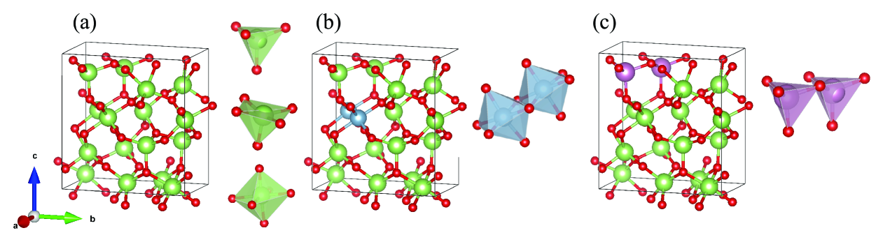
Two Ga atoms were replaced with Al (In) atoms at neighboring octahedrally (tetrahedrally) coordinated sites, and the structures were allowed to fully relax; these were found to be the energetically favorable substitutional sites for each respective cation (see Fig. 1). d-orbital electrons were included as valence in Ga and In atoms. Self-trapped holes were studied by removing an electron from the valence band. Subsequently, random shifts were imposed around a given lattice site (oxygen atom) were imposed [32, 33]; in the defect systems, the In/Al atoms were included in the shifted atoms. The system was then allowed to relax, while keeping symmetry unconstrained, and a final HSEsol calculation was performed to obtain the electronic and optical properties.
III Results and Discussions
III.1 Structural Properties
III.1.1 Neutral Bulk Parameters
The volume of pure at the PBEsol level was found to be 51.23 Å3, in good agreement with other simulations [32, 34] and experiment [35]. The equilibrium lattice parameters and volumes are summarized in Table 1. Isotropic compression (expansion) of the bulk volume occurs in the 12.5 Al (In) system, accounting for the smaller (larger) substitutional atoms compared to Ga.
| System | a (Å) | b (Å) | c (Å) | Volume (Å3) |
|---|---|---|---|---|
| - | 5.07 | 8.69 | 9.30 | 51.23 |
| 12.5 Al | 5.02 | 8.65 | 9.29 | 50.41 |
| 12.5 In | 5.11 | 8.77 | 9.38 | 52.54 |
III.1.2 Self-trapped Hole Relaxation
After full ionic relaxation, as shown in Fig. 2, the dopant Al atoms moved from the lowest energy octahedrally coordinated substitutional sites across the cell to tetrahedrally and pentahedrally coordinated sites. The larger cations (Ga and In), on the other hand, relaxed back to the equilibrium positions before a hole was added to the system.
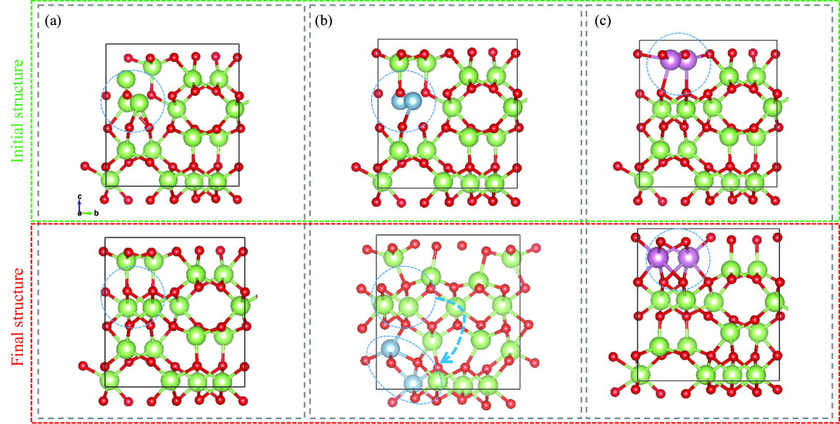
Notably, in the 12.5 Al system, a substantial distortion occurs with the inclusion of a STH, with the two Al atoms shifting, on average, approximately 5 Å from their unrelaxed starting positions into a new coordination environment. This shift is smaller in the 12.5 In system, with an average In-O bond change of 2 Å. This difference is consistent with the fact that the atomic radius of Al is only 80 of Ga’s, while the atomic radius of In is 10 larger than Ga. In the pure and 12.5 In systems, the cation atoms relaxed back towards their ground state position, within 0.1 Å of the relaxed position without a hole.
III.2 Electronic Properties
| System | Bandgap (eV) | (eV) | STH Level (eV) | Electron | Hole |
|---|---|---|---|---|---|
| 4.65 (direct, ) | 0.015 | 0.87 | 0.480 ( to Z) | -15.410 ( to Z) | |
| 12.5 Al | 4.89 (direct, ) | 2.157 | 0.74 | 0.434 ( to X) | -12.848 ( to X) |
| 0.341 ( to Y) | -10.900 ( to Y) | ||||
| 0.343 ( to Z) | -4.483 ( to Z) | ||||
| 12.5 | In 4.38 (indirect, T to ) | 0.912 | 0.84 | 0.408 ( to X) | -9.925 (T to R) |
| 4.40 (direct, ) | 0.320 ( to Y) | -15.53 (T to Z) | |||
| 0.327 ( to Z) |
The hole self-trapping energy () is calculated as the difference between the total energy of the unrelaxed, delocalized hole () and the total energy of the relaxed, localized hole (), given by
| (1) |
where a positive value indicates that STHs will form spontaneously; calculated electronic parameters are detailed in Table 2. The neutral system is least likely to form a STH with the lowest EST of 0.015 eV, while the inclusion of Al results in the largest positive value of 2.157 eV; both alloyed systems form STH spontaneously. The STH level as measured from the top of the valence band, related to neutral follows similar trends in the alloy systems, while the band gaps are opposite. In both, the STH level moves closer to the valence band maximum (VBM) as seen in Fig. 2; this is more pronounced in 12.5 Al. The band gap, however, increases for 12.5 Al while it decreases for 12.5 In, which is expected for the smaller/larger atomic substitution. The band edge effective masses were calculated using parabolic band fitting. The inclusion of alloys results in a breaking of the band edge degeneracy, resulting in anisotropic effective masses. The electron and hole masses are reduced with the inclusion of dopants, which is seen more in the dispersion that emerges in the normally flat valence bands. The effective mass in the (001) direction is reduced by a factor of three in the 12.5 Al system due to the smaller cation size, while the indirect gap edges see little change in the 12.5 In system. The electronic band structures in Fig. 3 shows the effects of dopants on the band gap. The band edge contributions remain relatively unchanged with the isoelectronic substitutions, and the effective mass of the conduction band is only slightly lighter for the alloyed systems. The band gap and dispersion are similar to other published results for the pure system, albeit using a different hybrid functional (B3LYP) [32].
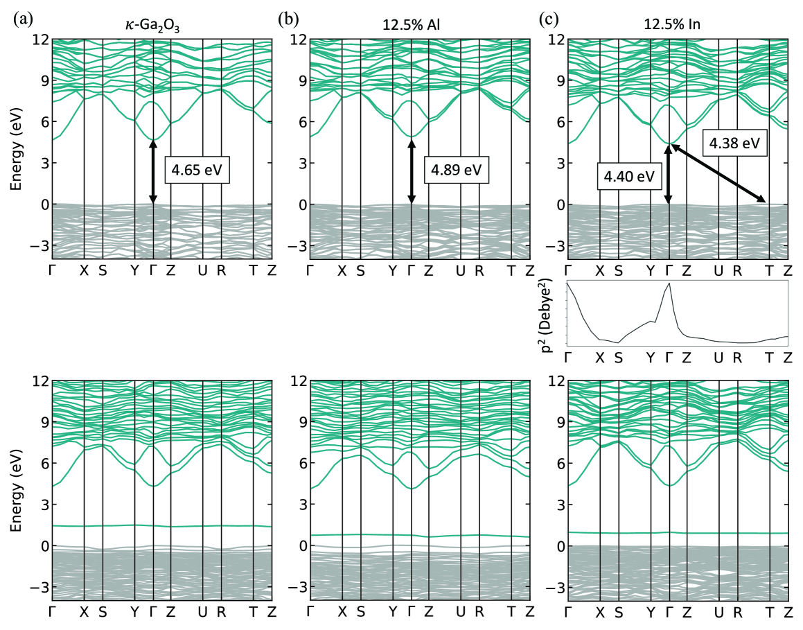
The band gap increases (decreases) with the inclusion of 12.5 Al (In) and remains direct in each system. A slightly smaller indirect band gap opens for 12.5 In; however, this is not the dominant transition at the VBM as seen in the plot of the transition probability in Fig. 3(c) (between the 12.5 In plots). The STH level is shown in the bottom row of Fig. 3 as the lowest dark cyan line, which represents the deep, hole, induced acceptor state. This state is shifted towards the VBM in both alloyed systems; more so for 12.5 Al. However, this band is still deep in both systems as the STH level is greater than 25 meV above the VBM. Each of these states correspond accordingly to the absorption onset seen in Fig. 6(f).
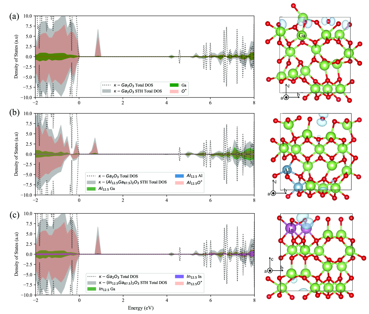
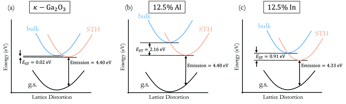
The hole state wavefunction in each system studied has a p-orbital characteristic and is localized around O near the defect site, as seen on the right in Fig. 4. In pure and 12.5 In, the hole is localized between the two cations which were shifted towards the O where the hole localizes; in the 12.5 Al system, the two Al move from their initial coordination and the hole follows, localizing on a nearby O atom instead of the one towards which the Al were initially shifted. The hole self-trapping energy () in neutral ( 0.02 eV) is an order of magnitude smaller than in the -phase value of 0.5 eV [10]. This difference likely arises from the more regular atomic stacking in the monoclinic crystal structure of , where holes experience greater steric confinement. This contrasts with the larger cavities present in the orthorhombic phase, which allow for potential hole delocalization. However, the presence of dopant atoms significantly increases the STH energy to 2.16 eV in the 12.5 Al system and 0.912 eV in the 12.5 In system, as seen in the configuration coordinate diagrams in Fig. 5. These values suggest that STHs will form spontaneously in all the studied orthorhombic systems, and their formation potential is further enhanced by the addition of isoelectronic dopants. The 12.5 Al value is an order of magnitude greater than the hDFT-simulated value of 0.24 eV for [16]. For the 12.5 In system, the simulated value of 0.91 eV, while closer, is still nearly four times larger than the reported bulk value of 0.25 eV in . This discrepancy is attributed to the larger lattice distortions present in the defect systems, which are predominantly . The bulk value for the -phase of is 0.53 eV, exceeding the bulk values of both dopant atoms [13]. Prior to this study, no values for the orthorhombic phase of have been reported.
III.3 Optical Properties
Emission is calculated as the difference between the equilibrium energy of the STH configuration and the same geometry with the hole removed (electron added back to the system). Emission values follow the same trend as the STH energy, where 12.5 Al (In) has a larger (smaller) value (4.48 eV for Al, 4.33 eV for In) than neutral (4.40 eV). These values are all larger than those for bulk monoclinic [13]. Fig. 5 shows the configuration coordinate diagrams for each system, highlighting the process of creation of a delocalized hole, the structural relaxation that leads to the trapping of the hole, and the emission due to the recombination of an electron-hole pair. This implies that a secondary process like lattice distortions (phonons) is required for electron-hole recombination to occur. Absorption occurs directly from the bulk equilibrium structure to the same structure with the delocalized hole, and then the configuration coordinate shifts to the distorted structure with the STH, where emission then occurs from the distorted STH structure to the same structure with the recombined electron and hole.
The calculated frequency dependent dielectric response was used to derive the standard optical parameters [36], which are shown in Fig. 6. STH formation in all systems results in a pronounced optical response within the visible spectrum. Pure has the largest STH emergent peak which is reduced due to the inclusion of Al or In (dashed lines in Fig. 6). Without a hole in the valence band, the inclusion of Al blue shifts the optical response, while In inclusion results in a red shift; however, STH formation red shifts each parameter regardless of the substitutional cation. This coupled with the positive for each alloyed system and the accompanying lattice distortions reveals the high likelihood of STH formation, even though there is a relative reduction in the peak height of each parameter in the visible spectrum.
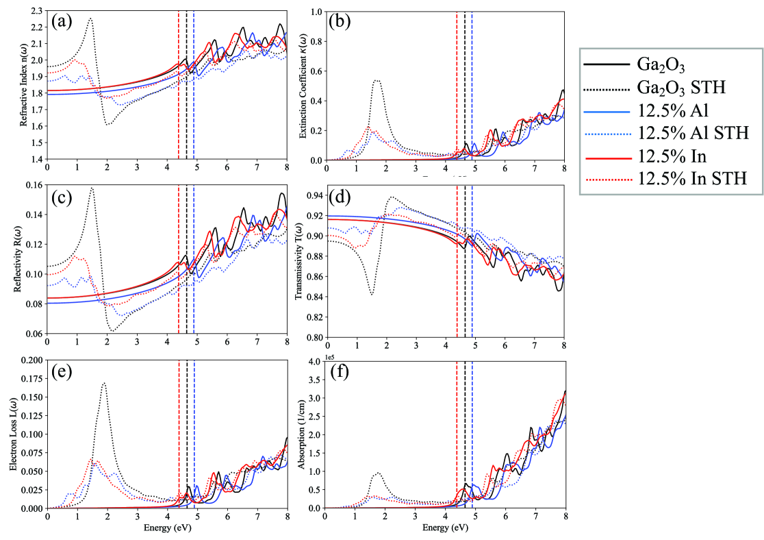
At = 6328 nm (E = 1.96 eV), the wavelength used to measure experimental refractive indices in wide band gap oxides [18], our simulated neutral and STH refractive index lines intersect for pure . This implies that the experimental value of the refractive index should be insensitive to the formation of small polarons for the undoped material; we calculated a value of n = 1.85, in good agreement with the experimental range of n = 1.85 – 1.96 [37]. For each alloyed system, however, the formation of a STH results in a reduction of the refractive index. We calculated neutral values for 12.5 Al and 12.5 In doping of n = 1.8, 1.85, respectively, which decreases to n = 1.76, 1.78 with the inclusion of a STH as seen in Fig. ( 6(a)). The extinction coefficient of each neutral system is zero throughout the visible spectrum, but is non-zero due to STH formation, resulting in an emergent visible light absorption peak in each material as seen in Figs. ( 6(b) and 6(f)). STH formation in each system reduces visible light transmission dramatically on the red edge of the visible light spectrum, which is accompanied by a non-zero absorption peak. Beyond 2 eV, however, the absorption peak diminishes, and the transmissivity increases for all systems. The emergent visible spectrum absorption is accompanied, in each system, by a non-zero electron loss, implying excitations will occur at lower energies than the band gap. No current simulations or EELS measurements from experiment exist yet for comparison.
IV Conclusions
This study investigates STH formation in orthorhombic and its alloys with Al and In using hDFT methods. Through analysis of structural, electronic, and optical properties, we demonstrate STH formation in each system, with the STH formation energy increasing upon the incorporation of alloying dopants. In all systems, positive STH energies correlate with lattice distortions, leading to hole localization on neighboring oxygen atoms with p-orbital character. The introduction of 12.5 isoelectronic Al or In alloying alters the electronic band gap and reduces the optical response in the visible light spectrum. Nevertheless, STH formation remains highly probable in each alloyed system due to the flat valence band, characterized by a heavy effective mass and composed of O 2p electrons. This observation, like that in the monoclinic phase, suggests that achieving p-type conductivity in orthorhombic through simple isoelectronic alloying is challenging, necessitating alternative strategies. However, orthorhombic and its alloys may offer advantages as higher-crystallinity transparent materials compared to the monoclinic phase.
Acknowledgements.
We acknowledge the Texas State University LEAP2 HPC resources used to do the computations in this work. EW and LS also thank encouraging initial discussions with Dr. R. Droopad from Texas State University who motivated the study of the orthorhombic phase of . The numpy [38], pymatgen [39], scipy [40], matplotlib [41], and sumo [42] python libraries as well as the VESTA [43] and vaspkit suites [44] were used to parse, post-process, and plot data. The scripts used and data generated in this study may be obtained from the authors upon reasonable request.References
- Emin [2013] D. Emin, Polarons (Cambridge University Press, 2013) pp. 43–48.
- Franchini et al. [2021] C. Franchini, M. Reticcioli, M. Setvin, and U. Diebold, Polarons in materials, Nature Reviews Materials 6, 560 (2021).
- Lyons et al. [2024] J. Lyons, D. Wickramaratne, and A. Janotti, Dopants and defects in ultra-wide bandgap semiconductors, Curr. Opin. Solid St. M. 30, 101148 (2024).
- Wenckstern [2017] H. Wenckstern, Group-iii sesquioxides: Growth, physical properties and devices, Adv. Electron. Mater. 3, 1600350 (2017).
- Kananen et al. [2017] B. Kananen, N. Giles, L. Halliburton, G. Foundos, K. Chang, and K. Stevens, Self-trapped holes in -ga2o3 crystals, J. Appl. Phys. 122, 215703 (2017).
- Nguyen and Radovanovic [2022] K. Nguyen and P. Radovanovic, Defects and impurities in colloidal ga2o3 nanocrystals: new opportunities for photonics and lighting, Can. J. Chem. 100, 1, 10.1139/cjc-2021-0203 (2022).
- Modak et al. [2024] S. Modak, A. Ruzin, A. Schulte, and L. Chernyak, Influence of energetic particles and electron injection on minority carrier transport properties in gallium oxide, Condens. Matter. 9, 2, 10.3390/condmat9010002 (2024).
- Armstrong et al. [2016] A. Armstrong, M. Crawford, A. Jayawardena, A. Ahyi, and S. Dhar, Role of self-trapped holes in the photoconductive gain of -gallium oxide schottky diodes, J. Appl. Phys 119, 103102 (2016).
- Yakimov [2021] E. Yakimov, Study of wide-gap semiconductors using electron-beam induced current method, Crystallogr. Rep. 66, 581 (2021).
- Frodason et al. [2020] Y. Frodason, K. Johansen, L. Vines, and J. Varley, Self-trapped hole and impurity-related broad luminescence in -ga2o3, J. Appl. Phys 127, 075701 (2020).
- Kioupakis et al. [2021] E. Kioupakis, S. Chae, K. Bushick, N. Pant, X. Zhang, and W. Lee, Theoretical characterization and computational discovery of ultra-wide-band-gap semiconductors with predictive atomistic calculations, J. Mater. Res. 36, 4616 (2021).
- Kaewmeechai et al. [2025] C. Kaewmeechai, J. Strand, and A. Shluger, Electronic structure and properties of trapped holes in crystalline and amorphous ga2o3, Phys. Rev. B 111, 10.1103/PhysRevB.111.035203 (2025).
- Varley et al. [2012] J. Varley, A. Janotti, C. Franchini, and C. Walle, Role of self-trapping in luminescence and p-type conductivity of wide-band-gap oxides, Phys. Rev. B 85, 10.1103/PhysRevB.85.081109 (2012).
- Tadjer et al. [2019] M. Tadjer, J. Lyons, N. Nepal, J. Freitas, Jr, A. Koehler, and G. M, Editors’ choice - review - theory and characterization of doping and defects in -ga2o3, ECS J. Solid State S.C. , 3187 (2019).
- Gake et al. [2019] T. Gake, Y. Kumagai, and F. Oba, First-principles study of self-trapped holes and acceptor impurities in ga2o3 polymorphs, Phys. Rev. Materials 3, 10.1103/PhysRevMaterials.3.044603 (2019).
- Lyons [2022] J. Lyons, Self-trapped holes and polaronic acceptors in ultrawide-bandgap oxides, J. Appl. Phys. 131, 025701 (2022).
- Labed et al. [2023] M. Labed, N. Sengouga, C. Prasad, M. Henini, and Y. Rim, On the nature of majority and minority traps in : A review, Mater. Today Phys. 36, 101155 (2023).
- Hassa et al. [2019] A. Hassa, H. Wenckstern, D. Splith, C. Sturm, M. Kneiß, V. Prozheeva, and M. Grundmann, Structural, optical, and electrical properties of orthorhombic thin films, APL Mater. 7, 022525 (2019).
- Shimada [2018] K. Shimada, First-principles study of crystal structure, elastic stiffness constants, piezoelectric constants, and spontaneous polarization of orthorhombic , Mater. Res. Express 5, 036502 (2018).
- Seacat et al. [2020] S. Seacat, J. Lyons, and H. Peelaers, Orthorhombic alloys of ga2o3 and al2o3, Appl. Phys. Lett. 116, 232102 (2020).
- Seacat et al. [2021] S. Seacat, J. Lyons, and H. Peelaers, Properties of orthorhombic ga2o3 alloyed with in2o3 and al2o3, Appl. Phys. Lett. 119, 042104 (2021).
- Wang et al. [2023] Y. Wang, J. Cao, H. Song, C. Zhang, Z. Xie, Y. Wong, and C. Tan, Polarization engineering of two-dimensional electron gas at heterostructure, Appl. Phys. Lett. 123, 10.1063/5.0172161 (2023).
- Wang et al. [2025] Y. Wang, Y. Guan, C. Zhang, J. Cao, X. Chen, Q. Ouyang, Y. Wong, G. Hu, and C. Tan, Indium alloying in for polarization and interfacial charge tuning, Appl. Phys. Lett. 126, 10.1063/5.0245828 (2025).
- Kresse and Hafner [1993] G. Kresse and J. Hafner, Ab initio molecular dynamics for liquid metals, Phys. Rev. B 47, 558 (1993).
- Kresse and Furthmüller [1996a] G. Kresse and J. Furthmüller, Efficiency of ab-initio total energy calculations for metals and semiconductors using a plane-wave basis set, Comp. Mater. Sci 6, 15 (1996a).
- Kresse and Furthmüller [1996b] G. Kresse and J. Furthmüller, Efficient iterative schemes for ab initio total-energy calculations using a plane-wave basis set, Phys. Rev. B 54, 11169 (1996b).
- Kresse and Joubert [1999] G. Kresse and D. Joubert, From ultrasoft pseudopotentials to the projector augmented-wave method, Phys. Rev. B 59, 1758 (1999).
- Perdew et al. [2008] J. Perdew, A. Ruzsinszky, G. Csonka, O. Vydrov, G. Scuseria, L. Constantin, X. Zhou, and K. Burke, Restoring the density-gradient expansion for exchange in solids and surfaces, Phys. Rev. Lett. 100, 136406 (2008).
- Schimka et al. [2011] L. Schimka, J. Harl, and G. Kresse, Improved hybrid functional for solids: the hsesol functional, J. Chem. Phys. 134, 024116 (2011).
- Welch et al. [2023] E. Welch, P. Borges, and L. Scolfaro, Hybrid density functional theory study of substitutional gd in , Physica B 651, 414558 (2023).
- Welch et al. [2024] E. Welch, M. Talukder, N. Martins, P. Borges, R. Droopad, and L. Scolfaro, Indium defect complexes in : a combined experimental and hybrid density functional theory study, J. Phys. D Appl. Phys. 57, 145302 (2024).
- Kim et al. [2018] J. Kim, D. Tahara, Y. Miura, and B. Kim, First-principle calculations of electronic structures and polar properties of , Appl. Phys. Express 11, 061101 (2018).
- Traiwattanapong et al. [2018] W. Traiwattanapong, A. Janotti, N. Umezawa, S. Limpijumnong, J. T-Thienprasert, and P. Reunchan, Self-trapped holes in batio3, J. Appl. Phys. 124, 10.1063/1.5036750 (2018).
- Lyons [2019] J. Lyons, Electronic properties of ga2o3 polymorphs, ECS J. Solid State SC 8, Q3226, 10.1149/2.0331907jss (2019).
- I. Cora [2017] E. I. Cora, The real structure of and its relation to -phase, CrystEngComm 19, 1509 (2017).
- Fox [2010] M. Fox, Optical Properties of Solids (OUP Oxford, 2010).
- Penman [2025] L. Penman, Comparative study of the optical properties of -, ‐, and , Phys. Status Solidi B 10.1002/pssb.202400615 (2025).
- Harris [2020] C. Harris, Array programming with numpy, Nature 585, 357 (2020).
- Jain et al. [2011] A. Jain, G. Hautier, C. Moore, S. Ong, C. Fischer, T. Mueller, K. Persson, and G. Ceder, A high-throughput infrastructure for density functional theory calculations, Comp. Mater. Sci. 50, 2295 (2011).
- Virtanen [2020] P. Virtanen, Scipy 1.0: fundamental algorithms for scientific computing in python, Nat. Methods 17, 261 (2020).
- Hunter [2007] J. Hunter, Matplotlib: A 2d graphics environment, comput, Comput. Sci. Eng. 9, 90, 10.1109/MCSE.2007.55 (2007).
- Ganose et al. [2018] A. Ganose, A. Jackson, D. Scanlon, and sumo, Command-line tools for plotting and analysis of periodic ab initio calculations, Journal of Open Source Software 3, 717 (2018).
- Momma and Izumi [2011] K. Momma and F. Izumi, Vesta 3 for three-dimensional visualization of crystal, volumetric and morphology data, J. Appl. Crystallogr. 44, 1272–1276 (2011).
- Wang et al. [2021] V. Wang, N. Xu, J.-C. Liu, G. Tang, and W.-T. Geng, Vaspkit: A user-friendly interface facilitating high-throughput computing and analysis using vasp code, Comput. Phys. Commun. 267, 108033, 10.1016/j.cpc.2021.108033 (2021).