Atomic Localization Fluorescent Microscopy
Abstract
Super-resolution microscopy has revolutionized the imaging of complex physical and biological systems by surpassing the Abbe diffraction limit. Recent advancements, particular in single-molecular localization microscopy (SMLM), have pushed localization below nanometer precision [1, 2, 3, 4, 5], by applying prior knowledge of correlated fluorescence emission from single emitters [6]. However, achieving a refinement from nm to Ångström demands a hundred-fold increase in collected photon signal [7, 6, 8]. This quadratic resource scaling imposes a fundamental barrier in SMLM, where the intense photon collection is challenged by photo-bleaching, prolonged integration times, and inherent practical constraints [9]. Here, we break this limit by harnessing the periodic nature of the atomic lattice structure. Specifically, applying this discrete grid imaging technique (DIGIT) in a quantum emitter system, we observe an exponential collapse of localization uncertainty once surpassing the host crystal’s atomic lattice constant. We further applied DIGIT to a large-scale quantum emitter array, enabling parallel positioning of each emitter through wide-field imaging. These results showcase that DIGIT unlocks a potential avenue to applications ranging from identifying solid-state quantum memories in crystals to the direct observation of optical transitions in the electronic structure of molecules.
I Introduction
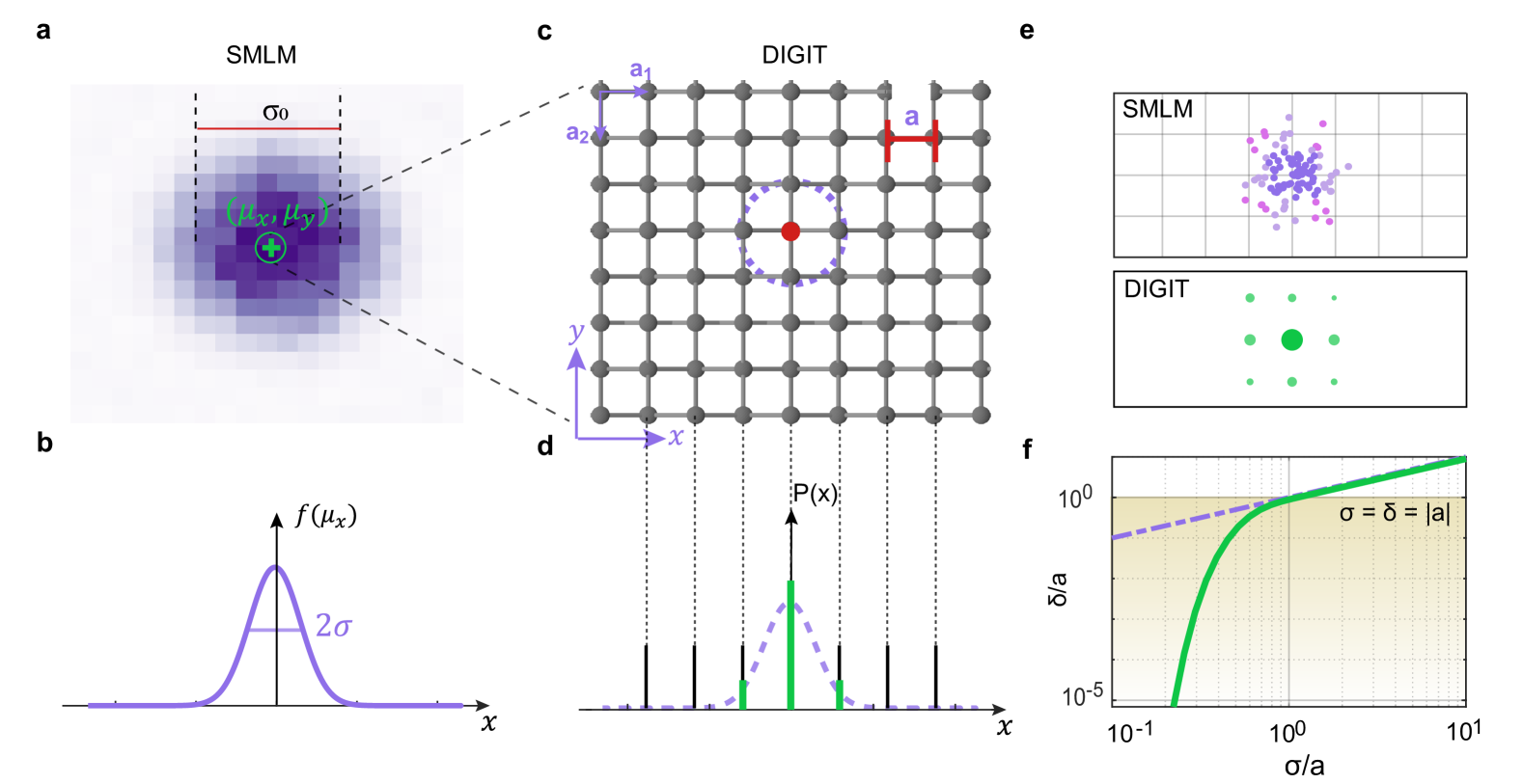
Optical super-resolution microscopy resolves the position of fluorescent emitters with a precision , that scales with the number of collected photons . Specifically, single-molecular localization microscopy (SMLM), which determines emitters’ positions by reconstructing their far-field point-spread functions (PSFs) [6], is fundamentally limited by , where is the standard deviation of the PSF, as shown in Fig. 1a. Recent works have achieved sub-nanometer localizing both fluorescent dyes [2, 4] and quantum emitters [10, 5, 11]. However, these approaches assume that independent measurements are made of a continuous position variable (Fig. 1b). In many physical systems, emitters reside at discrete lattice sites, prompting a breakdown of the continuous-space assumption. For example, crystal defects such as color centers are confined to specific atomic positions in the host lattice (Fig. 1c) [12, 13]. As localization approaches the lattice scale, it becomes essential to incorporate these positional constraints. In this work, we introduce a super-resolution technique that explicitly factors in the discrete nature of emitter positions, resulting in a new localization scaling of . This exponential enhancement pushes beyond the conventional limit, enabling localization approaching the atomic regime.
To illustrate this concept, Fig. 1d presents the transition from continuous to discrete localization. The purple dashed line represents the conventional SMLM localization distribution . By quantitatively linking the emitters’ underlying atomic lattice structure (black lines), the posterior localization distribution becomes discretized, sharply peaking at each lattice site with a periodicity (green lines). A detailed explanation of this incorporation of lattice constraints within a Bayesian framework is provided in Supplementary Information Sec. I.
The approach can be generalized to two dimensions where the position of each emitter is expressed not as but as an integer combination of lattice vectors: , where are lattice unit vectors and . We call this implementation the discrete grid imaging technique (DIGIT), and Fig 1e illustrates the resulting discrete localizations. The key advantage of DIGIT, as shown in Fig 1f, is that after approaches the lattice constant , the standard deviation of emitters’ estimated localization diminishes exponentially, beyond the polynomial scaling in conventional SMLM.
In this paper, we first demonstrate lattice-scale localization precision and accuracy using a diamond sample by reengineering the SMLM system. We then extend it to achieve atomic-scale localization using the Bayesian-based DIGIT approach. Additionally, we apply DIGIT to emitters and examine the enhancement requirements in a large-scale quantum system. Collectively, these advancements establish DIGIT as a competitive tool for attaining unprecedented precise measurements, ultimately paving the way to direct optical resolution of crystal and atomic features within quantum systems.
II Lattice-scale Accuracy and Precision
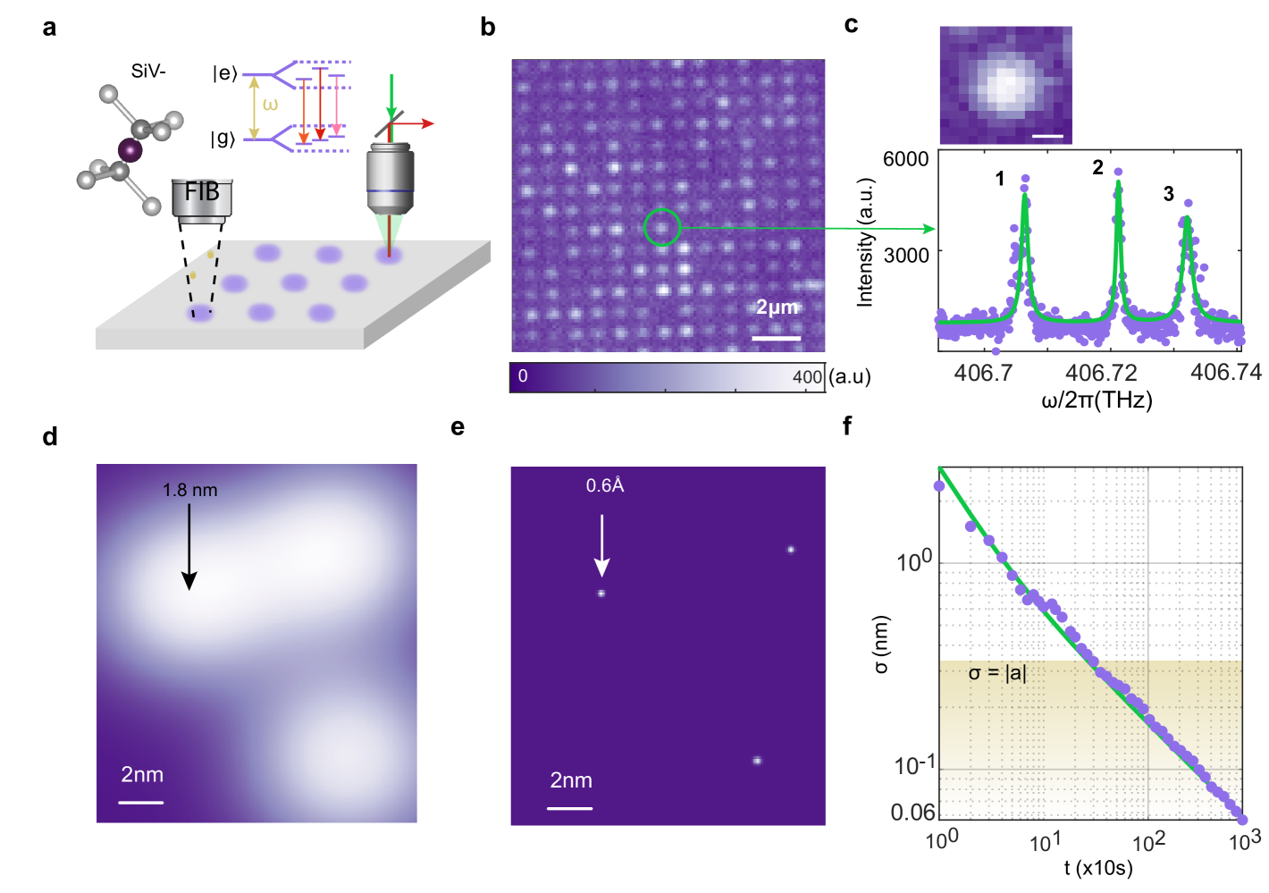
Diamond color centers (CCs) serve as exemplary systems for DIGIT because of their long-lived emission and well-defined locations within the diamond crystal lattice. Although previous studies have achieved sub-nanometer localization in diamond CCs [14, 15, 5, 1], several challenges remain in their imaging accuracy. These include mitigating the biases of the fitting model with fixed dipole nature of atomic transitions [16, 17, 18, 19] and drift-induced localization errors [20]. To address these challenges, we co-designed an end-to-end physical-digital twin system for SMLM, which accurately digitizes the experimental apparatus and optimizes its performance (Extended Data Fig. 2). By integrating this modeling into the microscope design and data acquisition, we achieve lattice-scale accuracy and precision.
The physical system involves a custom widefield cryogenic photoluminescence (PL) microscope (Fig. 2a) to image an array of silicon-vacancy centers (SiV) produced by focused-ion beam (FIB) implantation (See Methods). The farfield emission from SiVs is collected by an electron-multiplying charge-coupled device (EMCCD) camera. Fig. 2b shows the resulting PL image of SiV cluster arrays from off-resonant excitation.
To resolve individual SiV emitters beyond the diffraction limit, we applied prior knowledge of the natural inhomogeneous broadening of SiV transition energies [21] as illustrated in Fig. 2a. Specifically, we employed cryogenic photoluminescence excitation (PLE) by sweeping the excitation laser frequency across the zero-phonon line transitions and collecting light emitted into the phonon sideband on the EMCCD camera (see Methods). Fig. 2c presents the PLE spectrum of the cluster highlighted in Fig. 2b, revealing three distinct peaks with extracted resonance frequencies at THz, THz, THz. With the laser frequency locked at each , we subsequently re-acquired EMCCD images at extended integration times. For example, Fig. 2c shows an EMCCD image of SiV 1’s PSF with .
Next, we developed a comprehensive digital twin model to extract CCs’ positions from their emission profiles. Instead of a simplified 2D Gaussian fit, our digital twin accurately represents the entirety of the physical apparatus, correcting for system-induced biases to achieve Ångström-level localization accuracy and precision. Built on a fixed-dipole model governing far-field dipole emissions [22, 23], it further incorporates imperfections of the PLE setup such as optical aberrations, interpixel non-uniformity, electronic noise in the EMCCD, and setup drift. We verified the model’s accuracy by examining two orthogonally polarized optical transitions within a single SiV [21] and observed the two distinct PSFs overlap. Further details are provided in Supplementary Information Sec. III.
Fig. 2d and e compare the resulting localization probability density function derived from (d) a basic 2D Gaussian fit and (e) our digital twin model. In fig. 2d, the simple Gaussian approach yields a localization uncertainty of nm, insufficient to resolve two closely spaced emitters. However, by applying the accurate modeling, reduces to Å with integrating PSF over frames, as illustrated in Fig. 2e. Importantly, the three CCs are clearly spatially resolved. Fig. 2f plots the uncertainty of the highlighted emitter in Fig. 2e as a function of integration time . The standard error follows the shot-noise-limited scaling [24]. As increases, decreases past the threshold at the diamond lattice constant . The localization results for three emitters are provided in Supplementary Information Sec. IV.
III Atomic Localization with DIGIT
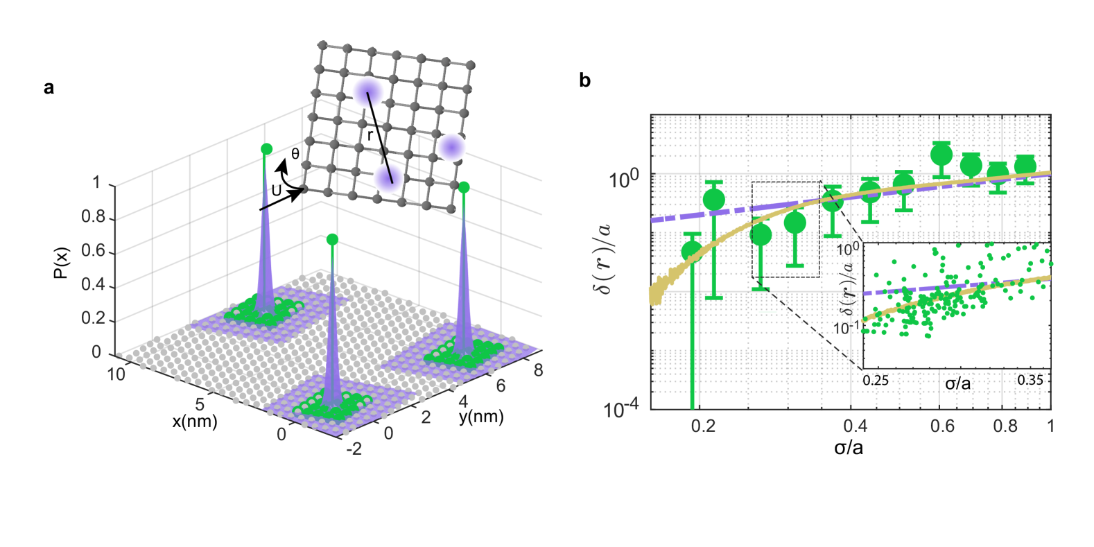
Building on the localization data from the previous section, we applied DIGIT to image SiVs with a Bayesian prior that encodes the diamond lattice coordinates. Since the PSF is collected along diamond’s [100] crystallographic direction, we simplified the intricate three-dimensional lattice by projecting it onto a two-dimensional plane along the [100] axis, as shown in Fig. 3a. We then computed after fitting the lattice positions via an affine transformation whose parameters are optimized through maximum likelihood estimation (see Extended Data Fig. 3).
Fig. 3a illustrates the resulting lattice positions (grey dots) and the new SiV localization determined by DIGIT. In contrast to the purple contour representing the conventional SMLM localization distribution , DIGIT localizations (green dots) exhibit discrete peaks that align well with specific lattice sites, reflecting the Bayesian incorporation of diamond’s periodic lattice structure.
Fig. 3b quantifies DIGIT by looking at the average localization deviation over three emitter pairs at different stages of . We compare the DIGIT results (green dots) with conventional SMLM represented (purple dashed line) and the Monte Carlo simulation of the DIGIT-based digital twin (yellow line). Our experimental result of aligns closely with the DIGIT simulation, surpassing the conventional limit of SMLM. Error bars represent the confidence intervals of localization uncertainty. The inset of Fig. 3b zooms in on the regime where DIGIT enhancement becomes pronounced. Each green dot represents an individual measurement at a specific . As a result, DIGIT enables localization entering an atomic regime of Å below the diamond lattice spacing, while conventional SMLM yields a mean uncertainty of Å for the same three emitter pairs. This 5-fold improvement over SMLM enables atomic resolution that would otherwise necessitate integration time 25 times longer.
IV Large-scale DIGIT
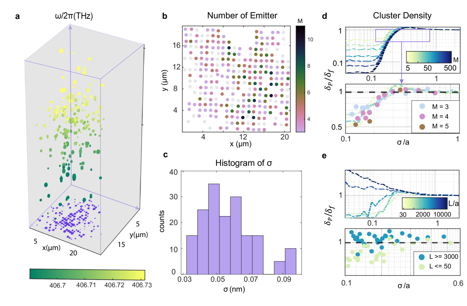
To explore the full capability of DIGIT, we extend the technique from one quantum cluster to multiple clusters across x m field of view. Using widefield PLE, we successfully resolved over single emitters within clusters. The localization of these emitters was facilitated by the pre-etched markers in diamond (Extended Data Fig. 1), which served as defined reference coordinates. Expanding to a wider field of view emphasizes the importance of the implementation of aberration corrections and camera interpixel non-uniformity calibrations to maintain high localization precision (see Supplementary Information Sec. III). Through the analysis of various clusters, we investigated the influence of parameters enabled by widefield measurements, particularly focusing on clusters’ density of states and brightness.
Fig. 4a presents a hyperspectral image of widefield PLE, spanning spatial and atomic transition frequency . We applied intensity-based region grouping to the PLE EMCCD image to distinguish individual emitters whose transitions range from to THz. Fig. 4b shows the reconstructed cluster density map, with each cluster color-coded by the emitter counts identified through PLE spectrum (See supplementary Information Sec. V). A detailed flowchart of the widefield PLE data analysis can be found in Extended Data Fig. 4.
Next we integrated frames at each resolved frequency and measured the localization uncertainty for each emitter, as summarized in Fig. 4c. Only CCs exhibiting sub-Ångström were counted for subsequent analysis. Emitters that did not meet this requirement have typically reduced brightness, exhibit blinking behavior [21], or experience non-uniformity widefield illumination [25], all of which contribute to worse localization uncertainty.
Figs. 4d and 4e present both numerical and experimental studies of the localization error enhancement across varying cluster densities. In Fig. 4d, we evaluate DIGIT’s performance with different emitter counts within a cluster. The simulation predicts that , indicating that the localization error can be effectively compensated for by higher emitter counts. This is because additional emitters help to refine lattice alignment through MLE. Experimentally, we examined three cluster densities , each closely matching the simulation prediction. This result confirms the collective advantage of dense-implanted clusters.
In Fig. 4e, we investigate for clusters with varying spatial separations at . Numerical simulations show that DIGIT’s advantage diminishes as L grows, because distinguishing the maximum likelihood lattice point from adjacent points requires increasingly precise estimates of the rotation angle , as . Achieving such high precision poses significant challenges for MLE methods due to computational and experimental limitations. Experimentally, this scenario is further complicated by strain-induced variations in lattice coherence length, which can result in uneven lattice structures and gaps that impede precise localization [26].
Nevertheless, by extending DIGIT to emitters across multiple clusters, we demonstrate its scalability and efficiency for parallel analysis. In contrast to scanning-based approaches that image each emitter individually, DIGIT processes many emitters simultaneously, achieving high-throughput localization.
V Discussion and Outlook
As the localization precision of conventional super-resolution microscopy approaches the length scale of electronic orbitals coupled to optical fields, it becomes essential to incorporate the atomic structure of samples as a Bayesian prior. Our demonstration of the DIGIT was made possible by achieving localization precision () comparable to the lattice constant (), allowing emitters to be accurately mapped to discrete lattice points rather than being confined to a continuous spatial domain. Furthermore, DIGIT provides a new precision scaling law: that is isotropic in all dimensions. Besides, parallelized DIGIT demonstrates its scalability by simultaneously localizing multiple emitters. To further access denser clusters, improved spectral resolution becomes critical. One promising strategy involves operating PLE without a repump laser so that emitters approach lifetime-limited spontaneous emission [27, 28].
Looking ahead, DIGIT has a direct application in diamond-based quantum information processes. For instance, the ability to achieve sub-Ångström localization enables in-situ tracking of emitters’ diffusion and interaction [29, 30, 31, 32], increases spatial storage density [33], and facilitates the generation and control of large cluster states made of locally coupled spins [34, 35]. Additionally, it is readily transferable to other periodic host materials, aiding to identify solid-state quantum memories. Potential candidates include point-like defects [36, 37, 38]; extended electronic orbitals in semiconductor quantum dots [39, 40], or molecules such as dibenzoterrylene, tetracene, or other complexes [41, 42, 43, 44, 45].
However, DIGIT is currently constrained to applications with well-characterized lattice structures. To overcome this limitation, our theoretical proposal for diamond suggests that with higher density CC, the atomic structure and the associated electronic orbital transitions can be learned, all from optical observation with zero-knowledge base (see Supplementary Information Sec. VI). Advanced computational techniques, such as deep learning of PSF from experimental observations [46, 47] and surrogate models [48], or generative AI methods such as adaptive model-based measurements, promise further acceleration.
Acknowledgments –We thank M.Mazaheri, Q.Peng for valuable input with the digital twin localization model. We thank C.S. Peng, A. Roy, H. Wang, J. Ren, Y. Liu for helpful discussions. We thank M.Mazaheri and V.Saggio for proofreading the manuscript. We acknowledge excellent technical support at the Massachusetts Institute of Technology (MIT) for MIT.Nano. Y.Yu performed FIB implantation, J. Daley performed evaporation medal growth. This work was supported in part by the National Science Foundation (NSF) Science-Technology Center (STC) Center for Integrated Quantum Materials (CIQM) under Grant No. DMR-1231319, by the NSF Engineering Research Center for Quantum Networks (CQN) awarded under Cooperative Agreement No. 1941583, and by the MITRE Moonshot Program. Y.D. acknowledges support by Mathworks fellowship.
Author Contribution –Y.D. conducted diamond fabrication, SiV implantation, digital twin development, localization analysis and measurements of the whole experiment. K.C.C. assisted with diamond fabrication. M.E.T assisted with building the wide-field SMLM, the dipole radiation model and digital twin verification. Q.G, Y.H, and D.R.E assisted with calibrating the camera photoresponse. Y.D and Q.G developed and implemented the Bayesian framework. Y.D, M.E.T and D.R.E conducted the theory proposal of optically resolved lattice structure. Y.D and D.R.E. conceived and supported the project. Y.D., M.E.T. and D.R.E wrote the manuscript with input from all authors.
Competing interests –The authors declare no competing financial interests.
Data availability –All the data that support the findings of this study are included in the Article and its Supplementary Information. Source data are available via figshare at 10.6084/m9.figshare.28281212
Code availability – Code for DIGIT principle and widefield DIGIT is available at: https://github.com/sophiaOnPoint/DIGIT
References
- Schröder et al. [2017] T. Schröder, M. E. Trusheim, M. Walsh, L. Li, J. Zheng, M. Schukraft, A. Sipahigil, R. E. Evans, D. D. Sukachev, C. T. Nguyen, J. L. Pacheco, R. M. Camacho, E. S. Bielejec, M. D. Lukin, and D. Englund, Scalable focused ion beam creation of nearly lifetime-limited single quantum emitters in diamond nanostructures, Nature Communications 8, 15376 (2017), publisher: Nature Publishing Group.
- Reinhardt et al. [2023] S. C. Reinhardt, L. A. Masullo, I. Baudrexel, P. R. Steen, R. Kowalewski, A. S. Eklund, S. Strauss, E. M. Unterauer, T. Schlichthaerle, M. T. Strauss, et al., Ångström-resolution fluorescence microscopy, Nature 617, 711 (2023).
- Lee et al. [2023] C. Lee, E. Z. Xu, K. W. Kwock, A. Teitelboim, Y. Liu, H. S. Park, B. Ursprung, M. E. Ziffer, Y. Karube, N. Fardian-Melamed, et al., Indefinite and bidirectional near-infrared nanocrystal photoswitching, Nature 618, 951 (2023).
- Pertsinidis et al. [2010] A. Pertsinidis, Y. Zhang, and S. Chu, Subnanometre single-molecule localization, registration and distance measurements, Nature 466, 647 (2010).
- Pfender et al. [2014] M. Pfender, N. Aslam, G. Waldherr, P. Neumann, and J. Wrachtrup, Single-spin stochastic optical reconstruction microscopy, Proceedings of the National Academy of Sciences 111, 14669 (2014), publisher: Proceedings of the National Academy of Sciences.
- Lelek et al. [2021] M. Lelek, M. T. Gyparaki, G. Beliu, F. Schueder, J. Griffié, S. Manley, R. Jungmann, M. Sauer, M. Lakadamyali, and C. Zimmer, ”single-molecule localization microscopy”, Nature Reviews Methods Primers 1, 39 (2021).
- Thompson et al. [2002] R. E. Thompson, D. R. Larson, and W. W. Webb, Precise nanometer localization analysis for individual fluorescent probes., Biophysical Journal 82, 2775 (2002).
- Bobroff [1986] N. Bobroff, Position measurement with a resolution and noise‐limited instrument, Review of Scientific Instruments 57, 1152 (1986), https://pubs.aip.org/aip/rsi/article-pdf/57/6/1152/19174299/1152_1_online.pdf .
- Sahl et al. [2024a] S. J. Sahl, J. Matthias, K. Inamdar, M. Weber, T. A. Khan, C. Brüser, S. Jakobs, S. Becker, C. Griesinger, J. Broichhagen, and S. W. Hell, Direct optical measurement of intramolecular distances with angstrom precision, Science 386, 180 (2024a), https://www.science.org/doi/pdf/10.1126/science.adj7368 .
- Rittweger et al. [2009] E. Rittweger, K. Y. Han, S. E. Irvine, C. Eggeling, and S. W. Hell, Sted microscopy reveals crystal colour centres with nanometric resolution, Nature Photonics 3, 144 (2009).
- Bersin et al. [2019a] E. Bersin, M. Walsh, S. L. Mouradian, M. E. Trusheim, T. Schröder, and D. Englund, Individual control and readout of qubits in a sub-diffraction volume, npj Quantum Information 5, 38 (2019a).
- Awschalom et al. [2018] D. D. Awschalom, R. Hanson, J. Wrachtrup, and B. B. Zhou, Quantum technologies with optically interfaced solid-state spins, Nature Photonics 12, 516 (2018).
- Aharonovich et al. [2016] I. Aharonovich, D. Englund, and M. Toth, Solid-state single-photon emitters, Nature photonics 10, 631 (2016).
- Chen et al. [2013] E. H. Chen, O. Gaathon, M. E. Trusheim, and D. Englund, Wide-field multispectral super-resolution imaging using spin-dependent fluorescence in nanodiamonds, Nano Letters 13, 2073 (2013), pMID: 23547791, https://doi.org/10.1021/nl400346k .
- Bersin et al. [2019b] E. Bersin, M. Walsh, S. L. Mouradian, M. E. Trusheim, T. Schroder, and D. Englund, Individual control and readout of qubits in a sub-diffraction volume, npj Quantum Information 5, 1 (2019b), publisher: Nature Publishing Group.
- Enderlein et al. [2006] J. Enderlein, E. Toprak, and P. R. Selvin, Polarization effect on position accuracy of fluorophore localization, Optics express 14, 8111 (2006).
- Backlund et al. [2016] M. P. Backlund, A. Arbabi, P. N. Petrov, E. Arbabi, S. Saurabh, A. Faraon, and W. Moerner, Removing orientation-induced localization biases in single-molecule microscopy using a broadband metasurface mask, Nature photonics 10, 459 (2016).
- Lew et al. [2013] M. D. Lew, M. P. Backlund, and W. E. Moerner, Rotational mobility of single molecules affects localization accuracy in super-resolution fluorescence microscopy, Nano Letters 13, 3967 (2013), pMID: 23360306, https://doi.org/10.1021/nl304359p .
- Ober et al. [2004] R. J. Ober, S. Ram, and E. S. Ward, Localization accuracy in single-molecule microscopy, Biophysical journal 86, 1185 (2004).
- Sahl et al. [2024b] S. J. Sahl, J. Matthias, K. Inamdar, M. Weber, T. A. Khan, C. Brüser, S. Jakobs, S. Becker, C. Griesinger, J. Broichhagen, et al., Direct optical measurement of intramolecular distances with angstrom precision, Science 386, 180 (2024b).
- Hepp et al. [2014] C. Hepp, T. Müller, V. Waselowski, J. N. Becker, B. Pingault, H. Sternschulte, D. Steinmüller-Nethl, A. Gali, J. R. Maze, M. Atatüre, and C. Becher, Electronic structure of the silicon vacancy color center in diamond, Phys. Rev. Lett. 112, 036405 (2014).
- Petrov et al. [2017] P. N. Petrov, Y. Shechtman, and W. E. Moerner, Measurement-based estimation of global pupil functions in 3d localization microscopy, Opt. Express 25, 7945 (2017).
- AXELROD [2012] D. AXELROD, Fluorescence excitation and imaging of single molecules near dielectric-coated and bare surfaces: a theoretical study, Journal of Microscopy 247, 147 (2012), https://onlinelibrary.wiley.com/doi/pdf/10.1111/j.1365-2818.2012.03625.x .
- Mortensen et al. [2010] K. I. Mortensen, L. S. Churchman, J. A. Spudich, and H. Flyvbjerg, Optimized localization analysis for single-molecule tracking and super-resolution microscopy, Nature methods 7, 377 (2010).
- Sutula et al. [2023] M. Sutula, I. Christen, E. Bersin, M. P. Walsh, K. C. Chen, J. Mallek, A. Melville, M. Titze, E. S. Bielejec, S. Hamilton, et al., Large-scale optical characterization of solid-state quantum emitters, Nature Materials 22, 1338 (2023).
- Tong et al. [2024] K. Tong, X. Zhang, Z. Li, Y. Wang, K. Luo, C. Li, T. Jin, Y. Chang, S. Zhao, Y. Wu, et al., Structural transition and migration of incoherent twin boundary in diamond, Nature 626, 79 (2024).
- Arjona Martínez et al. [2022] J. Arjona Martínez, R. A. Parker, K. C. Chen, C. M. Purser, L. Li, C. P. Michaels, A. M. Stramma, R. Debroux, I. B. Harris, M. Hayhurst Appel, E. C. Nichols, M. E. Trusheim, D. A. Gangloff, D. Englund, and M. Atatüre, Photonic indistinguishability of the tin-vacancy center in nanostructured diamond, Phys. Rev. Lett. 129, 173603 (2022).
- Ikeda et al. [2024] K. Ikeda, Y. Chen, P. Wang, Y. Miyamoto, T. Taniguchi, S. Onoda, M. Hatano, and T. Iwasaki, Charge state transition of spectrally stabilized tin-vacancy centers in diamond (2024), arXiv:2412.07087 [quant-ph] .
- Zu et al. [2021] C. Zu, F. Machado, B. Ye, S. Choi, B. Kobrin, T. Mittiga, S. Hsieh, P. Bhattacharyya, M. Markham, D. Twitchen, et al., Emergent hydrodynamics in a strongly interacting dipolar spin ensemble, Nature 597, 45 (2021).
- Mosavian et al. [2024] N. Mosavian, F. Hubert, J. Smits, P. Kehayias, Y. Silani, B. A. Richards, and V. M. Acosta, Super-resolution diamond magnetic microscopy of superparamagnetic nanoparticles, ACS Nano 18, 6523 (2024), pMID: 38369724, https://doi.org/10.1021/acsnano.3c12283 .
- Rendler et al. [2017] T. Rendler, J. Neburkova, O. Zemek, J. Kotek, A. Zappe, Z. Chu, P. Cigler, and J. Wrachtrup, Optical imaging of localized chemical events using programmable diamond quantum nanosensors, Nature communications 8, 14701 (2017).
- Xie et al. [2022] M. Xie, X. Yu, L. V. H. Rodgers, D. Xu, I. Chi-Durán, A. Toros, N. Quack, N. P. de Leon, and P. C. Maurer, Biocompatible surface functionalization architecture for a diamond quantum sensor, Proceedings of the National Academy of Sciences 119, e2114186119 (2022), https://www.pnas.org/doi/pdf/10.1073/pnas.2114186119 .
- Zhou et al. [2024] J. Zhou, J. Su, J. Guan, Y. Yang, W. Ji, M. Wang, F. Shi, K. Xia, Y. Wang, and J. Du, Terabit-scale high-fidelity diamond data storage, Nature Photonics , 1 (2024).
- Nemoto et al. [2014] K. Nemoto, M. Trupke, S. J. Devitt, A. M. Stephens, B. Scharfenberger, K. Buczak, T. Nöbauer, M. S. Everitt, J. Schmiedmayer, and W. J. Munro, Photonic architecture for scalable quantum information processing in diamond, Phys. Rev. X 4, 031022 (2014).
- Maurer et al. [2010] P. Maurer, J. R. Maze, P. Stanwix, L. Jiang, A. V. Gorshkov, A. A. Zibrov, B. Harke, J. Hodges, A. S. Zibrov, A. Yacoby, et al., Far-field optical imaging and manipulation of individual spins with nanoscale resolution, Nature Physics 6, 912 (2010).
- Ivády et al. [2017] V. Ivády, J. Davidsson, N. T. Son, T. Ohshima, I. A. Abrikosov, and A. Gali, Identification of si-vacancy related room-temperature qubits in silicon carbide, Phys. Rev. B 96, 161114 (2017).
- Koehl et al. [2011] W. F. Koehl, B. B. Buckley, F. J. Heremans, G. Calusine, and D. D. Awschalom, Room temperature coherent control of defect spin qubits in silicon carbide, Nature 479, 84 (2011).
- Stern et al. [2022] H. L. Stern, Q. Gu, J. Jarman, S. Eizagirre Barker, N. Mendelson, D. Chugh, S. Schott, H. H. Tan, H. Sirringhaus, I. Aharonovich, et al., Room-temperature optically detected magnetic resonance of single defects in hexagonal boron nitride, Nature communications 13, 618 (2022).
- Englund et al. [2007] D. Englund, A. Faraon, I. Fushman, N. Stoltz, P. Petroff, and J. Vučković, Controlling cavity reflectivity with a single quantum dot, Nature 450, 857 (2007).
- Srivastava et al. [2015] A. Srivastava, M. Sidler, A. V. Allain, D. S. Lembke, A. Kis, and A. Imamoğlu, Optically active quantum dots in monolayer wse2, Nature nanotechnology 10, 491 (2015).
- Wu et al. [2014] T. C. Wu, N. J. Thompson, D. N. Congreve, E. Hontz, S. R. Yost, T. Van Voorhis, and M. A. Baldo, Singlet fission efficiency in tetracene-based organic solar cells, Applied Physics Letters 104, 193901 (2014), https://pubs.aip.org/aip/apl/article-pdf/doi/10.1063/1.4876600/13084642/193901_1_online.pdf .
- Einzinger et al. [2019] M. Einzinger, T. Wu, J. F. Kompalla, H. L. Smith, C. F. Perkinson, L. Nienhaus, S. Wieghold, D. N. Congreve, A. Kahn, M. G. Bawendi, et al., Sensitization of silicon by singlet exciton fission in tetracene, Nature 571, 90 (2019).
- Akselrod et al. [2014] G. M. Akselrod, P. B. Deotare, N. J. Thompson, J. Lee, W. A. Tisdale, M. A. Baldo, V. M. Menon, and V. Bulović, Visualization of exciton transport in ordered and disordered molecular solids, Nature communications 5, 3646 (2014).
- Musavinezhad et al. [2024] M. Musavinezhad, J. Renger, J. Zirkelbach, T. Utikal, C. U. Hail, T. Basché, D. Poulikakos, S. Götzinger, and V. Sandoghdar, High-resolution cryogenic spectroscopy of single molecules in nanoprinted crystals, ACS Nano 18, 21886 (2024), pMID: 39011947, https://doi.org/10.1021/acsnano.4c02003 .
- Laorenza et al. [2021] D. W. Laorenza, A. Kairalapova, S. L. Bayliss, T. Goldzak, S. M. Greene, L. R. Weiss, P. Deb, P. J. Mintun, K. A. Collins, D. D. Awschalom, T. C. Berkelbach, and D. E. Freedman, Tunable cr4+ molecular color centers, Journal of the American Chemical Society 143, 21350 (2021), pMID: 34817994, https://doi.org/10.1021/jacs.1c10145 .
- Möckl et al. [2020] L. Möckl, A. R. Roy, and W. E. Moerner, Deep learning in single-molecule microscopy: fundamentals, caveats, and recent developments, Biomed. Opt. Express 11, 1633 (2020).
- Cao et al. [2024] R. Cao, N. S. Divekar, J. K. Nuñez, S. Upadhyayula, and L. Waller, Neural space–time model for dynamic multi-shot imaging, Nature Methods , 1 (2024).
- Rodr´ıguez et al. [2024] C. Rodríguez, S. Arlt, L. Möckl, and M. Krenn, Automated discovery of experimental designs in super-resolution microscopy with xlumina, Nature Communications 15, 1 (2024).
- Stallinga and Rieger [2010] S. Stallinga and B. Rieger, Accuracy of the gaussian point spread function model in 2d localization microscopy, Optics express 18, 24461 (2010).
- Burek et al. [2012] M. J. Burek, N. P. de Leon, B. J. Shields, B. J. M. Hausmann, Y. Chu, Q. Quan, A. S. Zibrov, H. Park, M. D. Lukin, and M. Lončar, Free-standing mechanical and photonic nanostructures in single-crystal diamond, Nano Letters 12, 6084 (2012), pMID: 23163557, https://doi.org/10.1021/nl302541e .
- Fu et al. [2010] K.-M. C. Fu, C. Santori, P. E. Barclay, and R. G. Beausoleil, Conversion of neutral nitrogen-vacancy centers to negatively charged nitrogen-vacancy centers through selective oxidation, Applied Physics Letters 96, 121907 (2010), https://pubs.aip.org/aip/apl/article-pdf/doi/10.1063/1.3364135/14664550/121907_1_online.pdf .
- Kenett and Bortman [2022] R. S. Kenett and J. Bortman, The digital twin in industry 4.0: A wide-angle perspective, Quality and Reliability Engineering International 38, 1357 (2022), https://onlinelibrary.wiley.com/doi/pdf/10.1002/qre.2948 .
VI Method
VI.1 Diamond fabrication
We first strain-relieved the surface of an electronic-grade, single-crystal diamond plate (Element 6) through plasma etching [50]. Next, we deposited a nm layer of silicon nitride (SiN) hard mask via plasma-enhanced chemical vapor deposition (PECVD). The SiN hard mask was then patterned with coordinate markers by electron-beam lithography and reactive ion etching. Subsequently, we employed inductively coupled reactive-ion etching (ICP-RIE) to transfer the pattern from the hard mask onto the diamond surface. After etching the diamond with oxygen plasma, we deposited a nm gold layer using thermal evaporation, followed by a lift-off procedure that removes the SiN mask.
VI.2 Ion implantation
Focused ion implantation was performed at the MIT Nano facility using FIB-SEM VELION (Raith). It is a FIB machine using an ExB filter and single ion implantation, using fast beam blanking. The ExB mass-filter separates out different ionic species and charge states from liquid metal alloy ion sources, providing the capability for implantation both Si and Ge at 35keV and 70keV. For the Si implantation discussed here, we used an GeSiAu liquid metal alloy ion source with typical Si beam currents ranging from 0.4 to 1 pA. Fast beam blanking allows direct control over the number of implanted ions. We determine the number of implanted ions by measuring the beam current and setting the pulse length to target a given number of ions per pulse. We used an effective areal dose of 75, 70 and 105 ions/spot for Si++ implantation at 70 keV with nm beam diameter. Stopping and Range of Ions in Matter(SRIM) simulations estimated an implantation depth of nm. After ion implantation, we annealed the sample at C under high vacuum ( mbar) for 2 h to form SiVs and eliminate other multi-vacancy defects. Finally, we submerged the diamond sample in boiling tri-acid treatment (1:1:1 nitric:perchloric:sulfuric) to remove residual graphite induced from annealing, and subsequently oxidized the surface in a oxygen atmosphere at 450 C for 4 h [51].
VI.3 Experimental Setup
The PLE SMLM measurements were performed at 4 K in a closed-cycle helium cryostat (Montana Instruments). A home-built wide-field microscope (Supplementary Fig. 1) collected the CCs’ fluorescence with a high-NA objective (Zeiss 100x. NA 0.95) and directed the emission to either an EMCCD (Cascade 1K) with a mm imaging lens or a single-mode fibre coupled to both an avalanche photodiode (PerkinElmer) and a spectrometer (Princeton Instruments). The effective pixel size is nm (after 1x1 binning). Super-resolution PLE was performed using a tunable laser (MSquared SolsTis) and a 532-nm green laser for charge state initialization. The resonant laser output passed through a bandpass filter (Semrock FF01-735/28) to minimize background fluorescence. The CCs’ emission was collected via a dichroic mirror and filtered in free space using bandpass filters (Semrock FF01-740/13). A three-axis closed-loop piezoelectric stage (Attocube ANC300) was used to control the position of the sample on the microscope stage.
VI.4 Widefield PLE
We performed widefield PLE of SiV centers by using acousto-optic modulators to deliver a resonant pulse and a 532 nm charge repump pulse. The resonant laser was swept across a GHz range in MHz increments, with its frequency stabilized via a HighFinesse WS7 wavemeter to ensure high spectral resolution. We optimized the signal-to-noise ratio (SNR) of SiV EMCCD imaging by choosing the following camera’s setting: acquisition time at s, binning = 1x1, electron amplification of in addition to the camera’s gain of .
VI.5 DIGIT Algorithm
Evaluation of in silico DIGIT precision with analytical and numerical simulations
We evaluate the performance of DIGIT with the following step-by-step algorithm:
(1) A grid of lattice sites with number of emitters randomly positioned is generated (ground truth).
(2) SMLM localization is modeled from a 2D Gaussian distribution with linewidth .
(3) Prior knowledge of lattice structure is modeled as a series of delta functions with spacing aligned with lattice periodicity.
(4) Using MLE to find the optimized lattice offset and rotation angle based on the SMLM localization.
(5) Posterior is calculated in the Bayesian framework based on likelihood and prior . The result is:
where .
(6) DIGIT localization precision is calculated by finding the standard deviation of .
Steps 1 to 5 are repeated for different values of , and to numerically study .
VI.6 DIGIT Localization
Extended Data Fig. 2 shows the digital-physical twin system we developed to localize the center of the EMCCD image. A digital twin is a virtual representation of a physical object that is updated with real-time process. Compared with a model fitting, the digital twin enriched it by using a live feedback to optimize the setup’s performance [52].
VI.6.1 Digital Twin
We constructed the digital twin starting from a dipole radiation model adapted from ref. [23]. We included the following parameters to analytically calculate the dipole’s far-field emission intensity : emitter’s position nm, emission polarization , system defocus and astigmatism, objective numerical aperture (NA), focal length, and working distance.
We further added a matrix that corrects environmental imperfection to . We used a calibration sample with 1x1 m grid pattern (EM-Tech M-1) to extract the conversion factor from pixel to absolute distance. We used the python package [distortion] to fit the grid pattern to correct for distortion in the EMCCD images. The full calibration details are covered in the Supplementary Information Sec. III.
Another significant correction concerned setup drift during measurements. We addressed this by implementing a Kalman filter to track and correct the drift trajectory over time. The Kalman filter is based on a state model (Gauss-Markov model), which characterizes the dynamics of gain and bias, and an observation model that minimizes the estimation error of the state position. The detailed algorithm is provided in the Supplementary Information Sec. III. We evaluated the effectiveness of our drift correction approach using Allan variance.
The digital twin further optimized imaging performance via a custom-built control system. Specifically, the system automatically adjusts individual mirrors to align both the tunable and green lasers so that their focal spots coincide according to the cost function . In addition, we minimized defocus by monitoring the point spread function (PSF) intensity and adjusting the piezo stage accordingly.
VI.6.2 Localization
We first corrected the EMCCD images based on the interpixel calibration, aberration and drift analysis, then we fitted the dipole radiation model based on a weighted MLE cost function to localize emitters’ center :
where is the dipole radiation model, is the corrected EMCCD image, and the weight is square root of pixel intensity to balance the information at the emission center and tail. We repeat this fitting for all independent measurements, and the theoretical SMLM bound of localization precision is:
where is the pixelization, is readout noise, is photon counts of the EMCCD image.
VI.7 Large-scale DIGIT Analysis
Extended Data Fig. 4 illustrates the workflow for localizing emitters across multiple clusters using DIGIT. First, we performed widefield PLE imaging and summed all frequency-step images to generate a single composite. A 2D Gaussian bandpass filter was then applied to enhance the SNR, with low-pass and high-pass cutoffs set by and , respectively. This filtered image was used to identify candidate emitter centers where each bright spot must have an apparent size within and (Supplementary Information Sec. V).
Having identified these candidate emitters, we defined a region of interest around each bright spot. We then extracted the fluorescence spectrum over the full frequency range and fitted each peak with a Lorentzian lineshape. Supplementary Fig. 11 shows examples of the PLE spectrum. Subsequently, our custom control software locked the laser to these resonance frequencies, and we re-acquired the corresponding point-spread functions (PSFs) for each emitter.
We then performed a least-squares fit to a 2D Gaussian model of each PSF. If the initial fit achieved an R-squared , we proceeded with the DIGIT-based (digital twin) fitting to refine the localization accuracy.