Thin-film superconducting NbTi microwave resonators for cryogenic thermometry
Abstract
Superconducting microwave resonators have recently gained a primary importance in the development of cryogenic applications, such as circuit quantum electrodynamics, electron spin resonance spectroscopy and particles detection for high-energy physics and astrophysics. In this work, we investigate the influence of the film thickness on the temperature response of microfabricated Nb50Ti50 superconducting resonators. S-shaped split ring resonators (S-SRRs), to thick, are designed to be electromagnetically coupled with standard Cu coplanar waveguides (CPWs) and their microwave properties are characterized at temperatures below . The combined contributions of the kinetic inductance increase and the decreasing loaded quality factor induce an optimum condition on the temperature sensitivity and resolution of the resonators, for thinner films. A noise equivalent temperature () as low as , at , is reported for thick resonators at . We also asses the possibility of implementing a multiplexed frequency readout, allowing for the simultaneous temperature tracking of several sensors along a single CPW. Such results demonstrate the possibility to perform a distributed cryogenic temperature monitoring, with a sub- resolution. In such a perspective, superconducting S-SRRs, eventually benefiting from an even higher , might be exploited to accurately monitor the on-chip temperature of devices operating in cryogenic conditions.
In the last decades, microwave systems operating at temperatures well below have experienced a growing interest from the scientific community. In this framework, superconducting thin-films have paved the way for novel techniques and devices relying on low temperature quantum phenomena. Among different technologies, superconducting resonators have proven to be key elements for the design of microwave kinetic inductance detectors (MKIDs)[1, 2, 3, 4, 5], circuit quantum electrodynamics architectures (QED)[6, 7, 8] and qubits[9, 10, 11, 12], ultra-low noise quantum parametric amplifiers[13, 14, 15] and detectors for electron spin resonance (ESR) spectroscopy[16, 17, 18, 19]. Dealing with all the aforementioned applications, the accurate monitoring of the on-chip temperature is crucial for ensuring the correct functioning of the device. Commercially-available cryogenic thermometers, as CERNOX®[20] or RuO2[21] thin-film thermistors, generally show temperature resolutions around , below .[22, 23] Superconducting materials have also been investigated as alternatives to perform cryogenic thermometry, with DC CMOS-compatible devices[24] and microwave resonators[25] having reported temperature resolutions, respectively, around and , for . More specifically, the superconducting properties in the microwave range can be exploited to realize resonators able to correlate changes in the cryogenic temperature to frequency shifts[25, 26, 27], with the potential of performing a temperature readout in parallel with the operation of the chip. The possibility of exploiting high quality factors, larger than 104, the absence of additional interconnections and the ease of performing an accurate on-chip temperature monitoring make superconducting microwave resonators an attractive alternative to more conventional cryo-thermistors.[25]
In this work, we report on the dependence of the temperature sensitivity and resolution of superconducting microresonators on the superconducting film thickness. The aim of this study is to provide guidelines for the optimization of the performances of cryogenic thermometers based on the variation of the thin-film kinetic inductance. As a matter of fact, our findings demonstrate that, even though thinner films increase the temperature sensitivity of the resonators, as depending on the increasing , an excessive thinning of the superconducting film also entails a drastic reduction of the quality factor, inducing an increase in the minimum detectable temperature variations. In such a sense, a trade-off between temperature sensitivity and resolution has to be carefully evaluated in the design phase, in order to determine an optimal film thickness.
The kinetic inductance of superconducting materials is an electronic-transport parameter originating from the low inertia of Cooper pairs, whose density significantly decreases for temperatures approaching the superconducting-to-normal critical transition.[28, 29, 30, 31] In particular, considering a thin-film superconducting resonator, with length , width and normal state surface resistance , it is possible to model the temperature influence on its resonance frequency, close to the transition temperature and in the low frequency regime , as[31, 32]
| (1a) | |||
| (1b) |
where is the superconducting energy gap and , while and stand, respectively, for the geometric inductance and capacitance of the resonator.
In order to study the influence of the film thickness on the temperature response of superconducting resonators, several Nb50Ti50 films, with the thickness ranging from to , are DC sputtered, at room temperature, on C-plane sapphire wafers. The choice for Nb50Ti50 resides on its transition parameters, showing critical DC field values as high as [33, 34, 35] and microwave ones larger than [36], reducing the influence of magnetic field fluctuations. Moreover, a bulk critical temperature up to [33, 37, 38, 39] makes this material suitable for temperature ranges commonly achieved by cryogenic applications based on liquid He (LHe) cooling. Sapphire is exploited as substrate material because of its exceptional microwave properties in ultra-cold environments,[40, 41, 42] as, for instance, a high dielectric constant around and an extremely low loss factor , down to . A lower bound for the surface kinetic inductance of such films is estimated through the at ,[31, 43] with the value of the different normal state surface resistances measured just above the critical transition by means of a 4-wires patterned structure. In Table 1 we report the estimated surface kinetic inductances. A maximum of pH/ is obtained for the thick film. The use of nitride-based superconducting thin-films, such as NbN and NbTiN[43, 44, 45] could lead to larger and, eventually, to better sensitivity and resolution when used for cryogenic thermometry.
| 111Extracted from a 4-wires V/I measurement. | 222Fitting parameters from the -based model presented in Eq. 1. | 222Fitting parameters from the -based model presented in Eq. 1. | 222Fitting parameters from the -based model presented in Eq. 1. | ||
| (nm) | () | () | () | ||
| 24 | 51 | 11 | 6.2 | 48 | 440 |
| 57 | 17 | 3.2 | 7.7 | 35 | 560 |
| 105 | 8.7 | 1.5 | 8.1 | 29 | 660 |
| 147 | 5.7 | 0.99 | 8.1 | 27 | 710 |
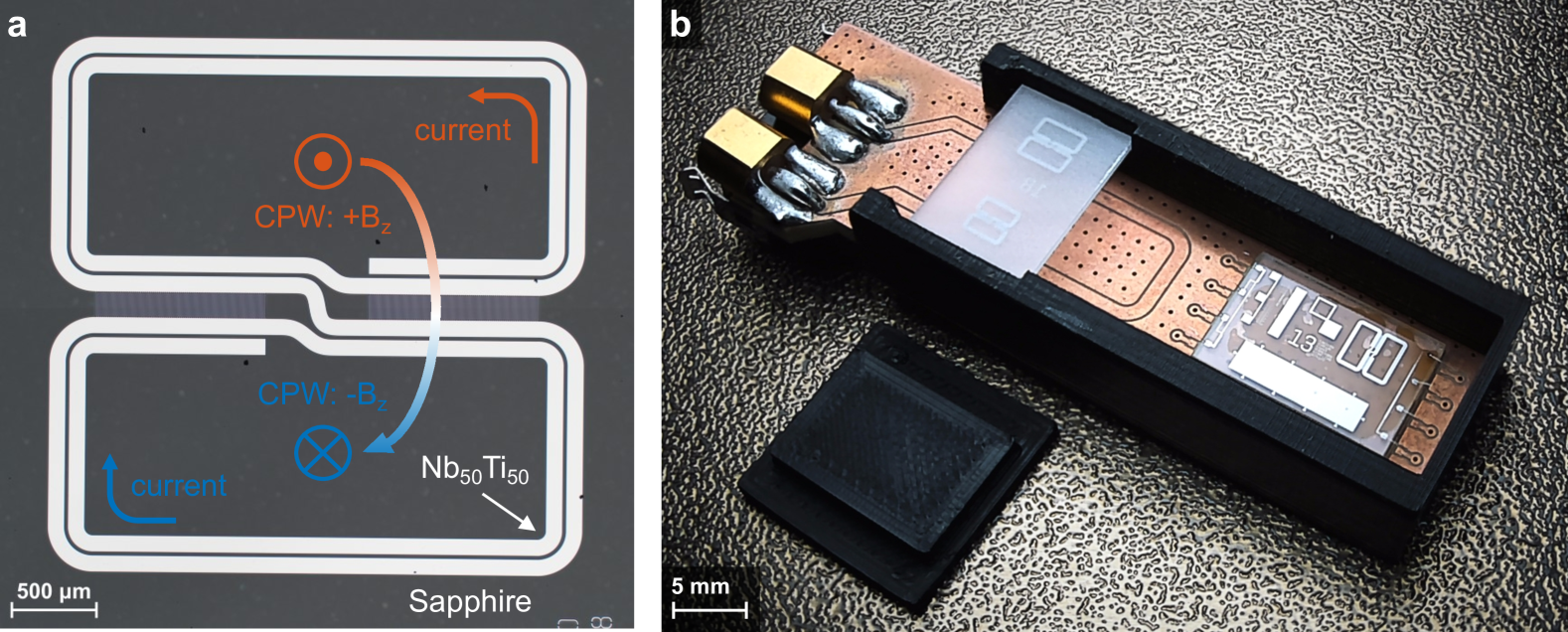
Among different planar geometries, S-shaped split ring resonators (S-SRRs) have been reported as ideal candidates for providing an optimal electromagnetic coupling with microwave coplanar waveguides (CPWs),[46, 47, 48] due to the possibility of exciting two counter-twisted inductive loops with antisymmetric magnetic field configurations [see Fig. 1]. In such a perspective, Nb50Ti50 S-SRRs are patterned on thick sapphire wafers, recurring to a combination of direct laser writing (DLW) photolithography and SF6/CHF3-based plasma etching. More details about the micro-fabrication of the thin-film resonators are reported in the supplementary material. The S-SRR geometry consists of 2-turns top and bottom loops ( ). The inductive stripe shows length and width values, respectively, equal to and . An inter-line gap of separates each turn, while two interdigitated capacitors (IDCs), made up of fingers (length: , width: , gap: ), are located between the two loops. Such additional capacitors are intended to maintain the compactness of the device, while lowering down its resonance frequency and limiting, therefore, the degradation of the quality factor induced by the increase of the superconducting surface resistance.[31, 30, 49]
COMSOL Multiphysics® finite element method (FEM) simulations are performed to optimize the S-SRR geometry for coupling inductively to a standard Cu grounded CPW (GCPW) and resonating approximatively around (see the supplementary material). The chips are coupled face-down to a GCPW by means of a 3D-printed polylactide (PLA) support, allowing to precisely place the S-SRRs with the two inductive loops centered on top of the transmission line gaps, as shown in Fig. 1. In such a configuration, the critical coupling parameter turns out to be the distance between the chip and the printed circuit board (PCB). In order to provide an optimal coupling, several tests are carried out in liquid He on the thick resonator, increasing from up to : as reported in the supplementary material, a distance value of is chosen, as it allows to excite the devices with approximately 50% of the transmitted power, still preserving loaded quality factor values larger than 104.
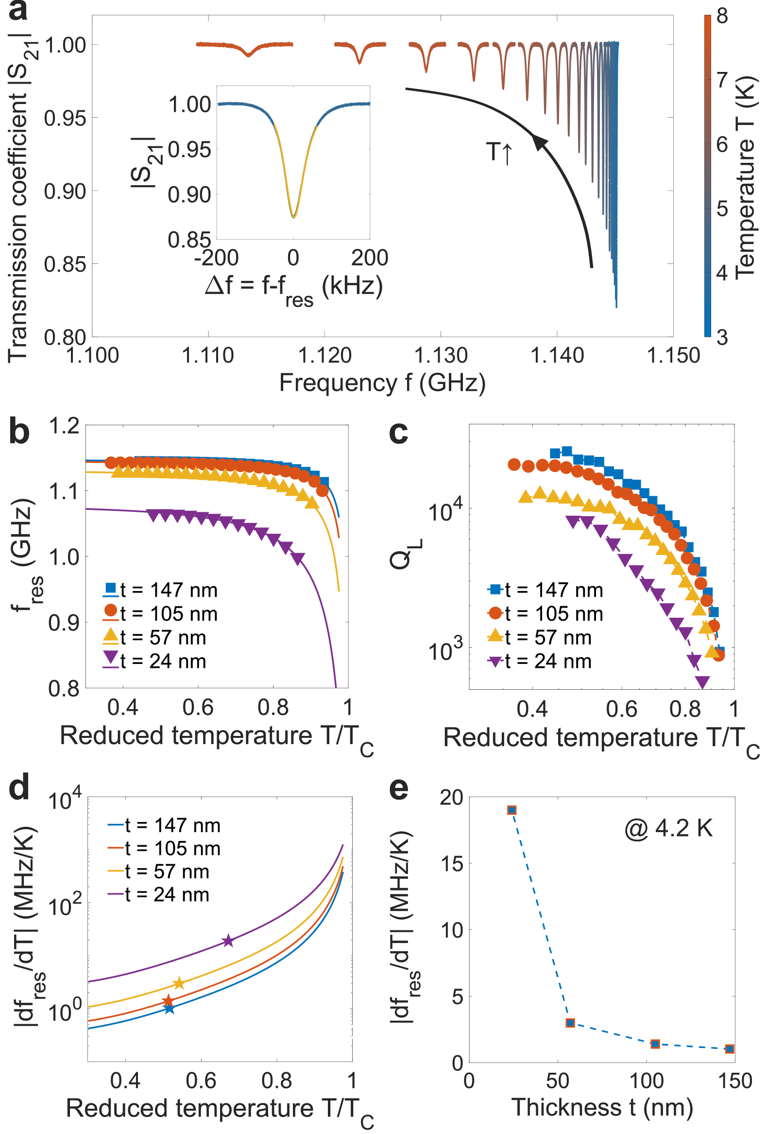
In order to investigate the temperature response of the resonators for different thicknesses, the S-SRRs are cooled down, in zero-field conditions, to temperatures as low as , by means of the variable temperature insert (VTI) of a dry superconducting cryomagnet. A 2-port vector network analyzer (VNA), directly connected in transmission to the PCB, is exploited to excite each device with a power of , allowing to record the S-parameters of the system. The temperature monitoring and control is achieved through the use of two CERNOX® thermometers and two heaters (see the supplementary material). In Fig. 2 we report the typical spectral response below . The effect of the microwave lines is eliminated by acquiring frequency scans at a temperature slightly above the superconducting transition and subtracting such backgrounds, in the complex domain, to the corresponding resonance signals.[50, 51] The values of the resonance frequency and the loaded quality factor are, then, extracted through a fit to a skewed-Lorentzian curve[52] (typically for ). The temperature response of the different S-SRRs is compared in Fig. 2, with the data-points being fitted to the model from Eq. 1. The resonance frequency of each device decreases as the temperature approaches the critical transition, consistently with the increase of the kinetic inductance term .[29] Moreover, an overall shift towards lower frequencies for is observed, which can probably be attributed to the increase of the geometric inductance , induced by the smaller cross-section of the thinner films. As described by Table 1, the increase in the term is well reflected by the evolution of such fitting parameter, as well as the critical temperature follows the saturation trend reported in literature for thicker films[29, 53]. Additionally, the loaded quality factor , even though showing values as high as 2.5104, is found to experience a decrease with respect to the reduction of the S-SRRs thickness, most probably due to the larger microwave resistance of the thinner films [see Fig. 2]. The temperature sensitivity of each resonator is also estimated, by means of the analytical model. The result is reported in Fig. 2 together with the evidence of the higher overall sensitivity for the devices characterized by larger values of kinetic inductance. In particular, an almost 20-fold larger sensitivity value of , is achieved, with respect to the thick S-SRR, for the thick one, at .
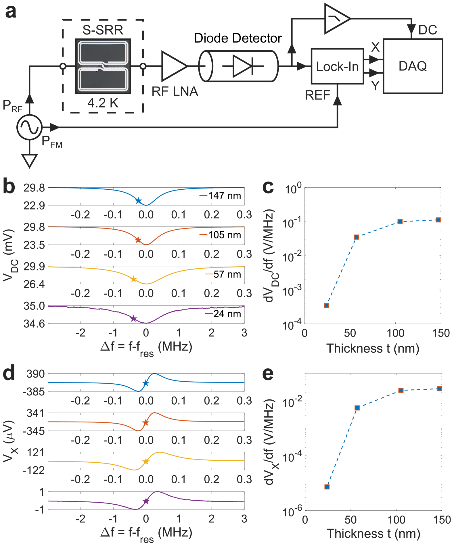
The temperature resolution of such superconducting devices is estimated at in a LHe dewar, in order to eliminate all sources of environmental noise related to temperature and remanent magnetic field fluctuations of the VTI chamber. Additionally, a more complex experimental setup, based on a frequency modulation (FM) lock-in detection scheme, is implemented [see Fig. 3]. A microwave signal generator is exploited to excite the S-SRRs with a power, frequency-modulated at with a deviation of . The choice of these three values is justified in the supplementary material. The microwave transmitted signal is amplified and converted into a DC value proportional to its amplitude with a microwave diode detector. The different components of the signal are then split, with the DC one further amplified, and the AC one detected by means of a lock-in amplifier, with a equivalent noise bandwidth (i.e. time constant). Finally, both DC, in-phase (X) and quadrature (Y) components are simultaneously acquired by a data acquisition (DAQ) board with a integration time (more details are presented in the supplementary material). Such a characterization setup is preferred to more conventional schemes, relying on VNAs[25, 43, 26] and homodyne readout systems[54, 55], to investigate the possible application of signal modulation techniques for reducing the influence of the instrumentation noise at lower frequencies. In Fig. 3 we report the frequency response of the DC component of the resonance signal. The dependance of the loaded quality factor on the film thickness, already observed in the previous variable-temperature experiments, affects the slope of the resonance curves. In particular, when thinning down the Nb50Ti50 film from to , we observe a reduction of by a factor of 20 and a reduction of the slope by a factor of 300 (from to ). Such a strong reduction of also impacts the response of the resonators in terms of the signal X component [see Fig. 3], where limiting values of and define the maximum slope conditions for the thickest and thinnest devices respectively.
The temperature resolution, or noise equivalent temperature (), expressed in , is defined as
| (2a) | |||
| (2b) |
where is the noise spectral density (in ), while is the temperature responsivity of the device (in ) as the product between the slope of the sensing signal (i.e either DC or X) and the temperature sensitivity of the resonance frequency. The low-frequency NSDs, below , are extracted by applying the fast Fourier transform (FFT) on a time monitoring of both the DC and X signals, with lock-in and DAQ integration times. Fig. 4 shows the frequency spectrum for the thick S-SRR, estimated by means of Eq. 2. The associated to the DC signal clearly shows a behavior below , which might be associated to the electronic noise coming from the setup instrumentation. In particular, a temperature resolution of about is achieved for such a signal at . The FM transfer of the sensing signal above the corner frequency, minimizes the influence of the instrumentation noise and allows to improve the temperature resolution of the device almost by a factor 10, with a around for the X signal at . The higher temperature sensitivity of thinner devices is counterbalanced by the degradation of the quality factor (i.e. curve slope ). As previously discussed, these two effects contribute in originating an optimum condition for the best temperature resolution. Considering the X signal evaluated at , a minimum of , among the investigated film thicknesses, is obtained for the thick resonator [see Fig. 4].
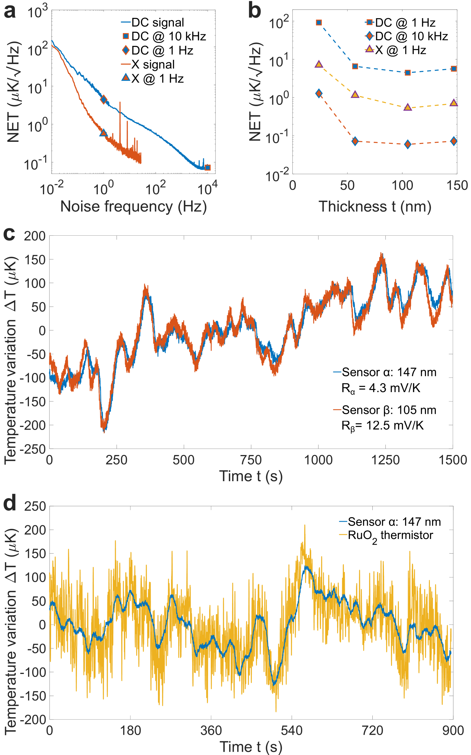
The temperature resolution below seems to be limited by low-frequency fluctuations in the order of , as shown in Fig. 4. The origin of such fluctuations is investigated by means of an experiment where two resonators are simultaneously measured (the and the thick ones). As fully described in the supplementary material, the two S-SRRs are individually excited by the same GCPW at their corresponding resonance frequencies (i.e. and , respectively) by two distinct microwave generators, modulating their excitations by two distinct modulation frequencies (i.e. and , respectively). Two lock-in amplifiers are used to perform the FM synchronous demodulation. Once normalized to the respective temperature responsivities , the responses of the two sensors show an almost identical time evolution, indicating that such low-frequency fluctuations might originate from a global common physical stimulus rather than from a noise source intrinsic to each sensor. Additionally, the coincidence of the two temperature estimations, originating from two sensors having significantly different responsivities, suggests the signal variations are associated to temperature-related phenomena. These hypotheses are confirmed by a final experiment, where the temperature inside the LHe dewar is simultaneously monitored by means of the thick S-SRR and a commercial sensor relying on a different physical principle, in particular a RuO2 thermistor[56]. As shown in Fig. 4, the thermistor response follows the resonator, especially over the largest fluctuations around . The technical details concerning this experiment are reported in the supplementary material.
In conclusion, we have fabricated and tested a set of temperature-sensitive Nb50Ti50 superconducting S-SRRs, generally showing for , in order to investigate the influence of the thin-film thickness on the resonance frequency shifts induced by the change of their kinetic inductance . In particular, the thinnest device exhibits the highest temperature sensitivity of , due to its larger value of surface kinetic inductance. However, the significant reduction in the loaded quality factor for thinner films entails a reduction of the maximum slope for the sensing DC and X curves, inducing an optimum condition at intermediate thickness values, when evaluating the temperature resolution of the devices. In this perspective, we have exploited frequency modulation and lock-in detection to assess the possibility to reach a sub- temperature resolution for such devices. The possibility to excite different resonators with the same microwave transmission line, while simultaneously tracking their temperature responses, have also been successfully demonstrated. Noise equivalent temperatures as low as are reported at in liquid He for a thick S-SRR. We believe that such superconducting devices, eventually benefiting from higher kinetic inductance films and entailing multiplexed readout schemes, could find applications in the measurement of distributed on-chip cryogenic temperatures.
SUPPLEMENTARY MATERIAL
The supplementary material contains additional information about the following topics:
-
S1.
Microfabrication process flow and SEM/AFM characterization of the patterned S-SRRs;
-
S2.
FEM microwave simulation of the resonance mode for the S-SRR geometry;
-
S3.
Experimental determination of the S-SRR-to-GCPW coupling distance in a LHe dewar;
-
S4.
VTI temperature calibration of the S-SRRs;
-
S5.
Determination of the modulation , and parameters in a LHe dewar;
-
S6.
Simultaneous temperature monitoring in a LHe dewar, by means of two different S-SRRs;
-
S7.
Simultaneous temperature monitoring in a LHe dewar, by means of an S-SRR and a RuO2 thermistor.
ACKNOWLEDGEMENTS
The authors thank the EPFL Center of Micro/Nanotechnology (CMi), in particular Cyrille Hibert, Julien Dorsaz, Niccolò Piacentini, Joffrey Pernollet and Adrien Toros, for the facility support provided during the microfabrication processing. We would also like to acknowledge Nergiz Sahin-Solmaz and Biranche Tandon for the fruitful discussions. This work has received funding from the Swiss National Science Foundation (SNSF), under the AMBIZIONE program (Project "Cryogenic Thermometry based on Superconducting Microwave Resonators", grant agreement No. PZ00P2_193361).
DATA AVAILABILITY
The data that support the findings of this study are available from the corresponding author upon reasonable request.
CREDITS
The following article has been submitted to Applied Physics Letters. After it is published, it will be found at Link.
REFERENCES
References
- Audley, Kelley, and Rawley [1993] M. D. Audley, R. L. Kelley, and G. L. Rawley, “A prototype kinetic inductance thermometer for X-ray calorimetry,” J. Low. Temp. Phys. 93, 245–250 (1993).
- Day et al. [2003] P. K. Day, H. G. LeDuc, B. A. Mazin, A. Vayonakis, and J. Zmuidzinas, “A broadband superconducting detector suitable for use in large arrays,” Nature 425, 817–821 (2003).
- Maloney et al. [2010] P. R. Maloney, N. G. Czakon, P. K. Day, T. P. Downes, R. Duan, J. Gao, J. Glenn, S. R. Golwala, M. I. Hollister, H. G. LeDuc, B. A. Mazin, S. G. McHugh, O. Noroozian, H. T. Nguyen, J. Sayers, J. A. Schlaerth, S. Siegel, J. E. Vaillancourt, A. Vayonakis, P. Wilson, and J. Zmuidzinas, “MUSIC for sub/millimeter astrophysics,” in Millimeter, Submillimeter, and Far-Infrared Detectors and Instrumentation for Astronomy V, Vol. 7741 (2010) p. 77410F.
- Austermann et al. [2018] J. E. Austermann, J. A. Beall, S. A. Bryan, B. Dober, J. Gao, G. Hilton, J. Hubmayr, P. Mauskopf, C. M. McKenney, S. M. Simon, J. N. Ullom, M. R. Vissers, and G. W. Wilson, “Millimeter-wave polarimeters using kinetic inductance detectors for TolTEC and beyond,” J. Low. Temp. Phys. 193, 120–127 (2018).
- Dibert et al. [2022] K. Dibert, P. Barry, Z. Pan, A. Anderson, B. Benson, C. Chang, K. Karkare, J. Li, T. Natoli, M. Rouble, E. Shirokoff, A. Stark, and the South Pole Telescope Collaboration, “Development of MKIDs for measurement of the cosmic microwave background with the South Pole Telescope,” J. Low. Temp. Phys. 209, 363–371 (2022).
- Wallraff et al. [2004] A. Wallraff, D. I. Schuster, A. Blais, L. Frunzio, R.-S. Huang, J. Majer, S. Kumar, S. M. Girvin, and R. J. Schoelkopf, “Strong coupling of a single photon to a superconducting qubit using circuit quantum electrodynamics,” Nature 431, 162––167 (2004).
- Göppl et al. [2008] M. Göppl, A. Fragner, M. Baur, R. Bianchetti, S. Filipp, J. M. Fink, P. J. Leek, G. Puebla, L. Steffen, and A. Wallraff, “Coplanar waveguide resonators for circuit quantum electrodynamics,” J. Appl. Phys. 104, 113904 (2008).
- Scarlino et al. [2019] P. Scarlino, D. J. van Woerkom, A. Stockklauser, J. V. Koski, M. C. Collodo, S. Gasparinetti, C. Reichl, W. Wegscheider, T. Ihn, K. Ensslin, and A. Wallraff, “All-microwave control and dispersive readout of gate-defined quantum dot qubits in circuit quantum electrodynamics,” Phys. Rev. Lett. 122, 206802 (2019).
- Kjaergaard et al. [2020] M. Kjaergaard, M. E. Schwartz, J. Braumüller, P. Krantz, J. I.-J. Wang, S. Gustavsson, and W. D. Oliver, “Superconducting qubits: current state of play,” Annu. Rev. Condens. Matter Phys. 11, 369–395 (2020).
- Koch et al. [2007] J. Koch, T. M. Yu, J. Gambetta, A. A. Houck, D. I. Schuster, J. Majer, A. Blais, M. H. Devoret, S. M. Girvin, and R. J. Schoelkopf, “Charge-insensitive qubit design derived from the Cooper pair box,” Phys. Rev. A 76, 042319 (2007).
- Schreier et al. [2008] J. A. Schreier, A. A. Houck, J. Koch, D. I. Schuster, B. R. Johnson, J. M. Chow, J. M. Gambetta, J. Majer, L. Frunzio, M. H. Devoret, S. M. Girvin, and R. J. Schoelkopf, “Suppressing charge noise decoherence in superconducting charge qubits,” Phys. Rev. B 77, 180502 (2008).
- Barends et al. [2014] R. Barends, J. Kelly, A. Megrant, A. Veitia, D. Sank, E. Jeffrey, T. C. White, J. Mutus, A. G. Fowler, B. Campbell, Y. Chen, Z. Chen, B. Chiaro, A. Dunsworth, C. Neill, P. O’Malley, P. Roushan, A. Vainsencher, J. Wenner, A. N. Korotkov, A. N. Cleland, and J. M. Martinis, “Superconducting quantum circuits at the surface code threshold for fault tolerance,” Nature 508, 500–503 (2014).
- Vissers et al. [2016] M. R. Vissers, R. P. Erickson, H.-S. Ku, L. Vale, X. Wu, G. C. Hilton, and D. P. Pappas, “Low-noise kinetic inductance traveling-wave amplifier using three-wave mixing,” Appl. Phys. Lett. 108, 012601 (2016).
- Aumentado [2020] J. Aumentado, “Superconducting parametric amplifiers: the state of the art in Josephson parametric amplifiers,” IEEE Microw. Mag. 21, 45–59 (2020).
- Frasca et al. [2024] S. Frasca, C. Roy, G. Beaulieu, and P. Scarlino, “Three-wave-mixing quantum-limited kinetic inductance parametric amplifier operating at 6 T near 1 K,” Phys. Rev. Appl. 21, 024011 (2024).
- Bienfait et al. [2016] A. Bienfait, J. J. Pla, Y. Kubo, M. Stern, X. Zhou, C. C. Lo, C. D. Weis, T. Schenkel, M. L. W. Thewalt, D. Vion, D. Esteve, B. Julsgaard, K. Mølmer, J. J. L. Morton, and P. Bertet, “Reaching the quantum limit of sensitivity in electron spin resonance,” Nat. Nanotechnol. 11, 253–257 (2016).
- Ranjan et al. [2020] V. Ranjan, S. Probst, B. Albanese, T. Schenkel, D. Vion, D. Esteve, J. J. L. Morton, and P. Bertet, “Electron spin resonance spectroscopy with femtoliter detection volume,” Appl. Phys. Lett. 116, 184002 (2020).
- Artzi et al. [2021] Y. Artzi, Y. Yishay, M. Fanciulli, M. Jbara, and A. Blank, “Superconducting micro-resonators for electron spin resonance - the good, the bad, and the future,” J. Mag. Res. 334, 107102 (2021).
- Akhmetzyanov et al. [2023] D. Akhmetzyanov, T. W. Borneman, I. Taminiau, S. Sadeghi, H. R. Mohebbi, and D. G. Cory, “Electron spin resonance spectroscopy using a Nb superconducting resonator,” Appl. Phys. Lett. 123, 224002 (2023).
- Courts and Swinehart [2003] S. S. Courts and P. R. Swinehart, “Review of Cernox™ (Zirconium Oxy-Nitride) Thin-Film Resistance Temperature Sensors,” AIP Conf. Proc. 684, 393–398 (2003).
- Myers, Li, and Csáthy [2021] S. A. Myers, H. Li, and G. A. Csáthy, “A ruthenium oxide thermometer for dilution refrigerators operating down to 5 mK,” Cryogenics 119, 103367 (2021).
- Holmes and Courts [1992] D. S. Holmes and S. S. Courts, “Resolution and accuracy of cryogenic temperature measurements,” Temperature: Its Measurement and Control in Science and Industry 6, 1225–1230 (1992).
- Yeager and Courts [2001] C. J. Yeager and S. S. Courts, “A review of cryogenic thermometry and common temperature sensors,” IEEE Sens. J. 1, 352–360 (2001).
- Noah et al. [2024] G. M. Noah, T. H. Swift, M. de Kruijf, A. Gomez-Saiz, J. J. L. Morton, and M. F. Gonzalez-Zalba, “CMOS on-chip thermometry at deep cryogenic temperatures,” Appl. Phys. Rev. 11, 021414 (2024).
- Wheeler et al. [2020] J. Wheeler, M. R. Vissers, M. Malnou, J. Hubmayr, J. N. Ullom, and J. Gao, “Sub-kelvin thermometer for on-chip measurements of microwave devices utilizing two-level systems in superconducting microresonators,” Appl. Phys. Lett. 117, 192601 (2020).
- Yu et al. [2022] H. Yu, L. Jing, T. Hua, and W. Xu, “Temperature and power characteristics of quarter-wavelength superconducting coplanar waveguide resonator,” SN Appl. Sci. 4, 67 (2022).
- Nulens et al. [2023] L. Nulens, N. Lejeune, J. Caeyers, S. Marinković, I. Cools, H. Dausy, S. Basov, B. Raes, M. J. Van Bael, A. Geresdi, A. V. Silhanek, and J. Van de Vondel, “Catastrophic magnetic flux avalanches in NbTiN superconducting resonators,” Commun. Phys. 6, 267 (2023).
- Gorter and Casimir [1934] C. J. Gorter and H. Casimir, “On supraconductivity I,” Physica 1, 306–320 (1934).
- Watanabe, Yoshida, and Kohjiro [1994] K. Watanabe, K. Yoshida, and T. A. Kohjiro, “Kinetic inductance of superconducting coplanar waveguides,” Jpn. J. Appl. Phys. 33, 5708 (1994).
- Hein [2001] M. A. Hein, “Microwave properties of superconductors,” in Microwave superconductivity, edited by H. Weinstock and M. Nisenoff (Springer Netherlands, Dordrecht, 2001) pp. 21–53.
- Tinkham [2004] M. Tinkham, Introduction to superconductivity, 2nd ed. (Dover, Mineola, N.Y., 2004).
- Annunziata et al. [2010] A. J. Annunziata, D. F. Santavicca, L. Frunzio, G. Catelani, M. J. Rooks, A. Frydman, and D. E. Prober, “Tunable superconducting nanoinductors,” Nanotechnol. 21, 445202 (2010).
- Bychkov, Herzog, and Khukhareva [1981] Y. F. Bychkov, R. Herzog, and I. S. Khukhareva, “Thermal conductivity and electrical resistivity of NbTi alloys at low temperatures,” Cryogenics 21, 741–745 (1981).
- Bottura [2000] L. Bottura, “A practical fit for the critical surface of NbTi,” IEEE Trans. Appl. Supercond. 10, 1054–1057 (2000).
- Ghigo et al. [2023] G. Ghigo, D. Torsello, L. Gozzelino, M. Fracasso, M. Bartoli, C. Pira, D. Ford, G. Marconato, M. Fretto, I. De Carlo, N. Pompeo, and E. Silva, “Vortex dynamics in NbTi films at high frequency and high DC magnetic fields,” Sci. Rep. 13, 9315 (2023).
- Russo et al. [2023] R. Russo, A. Chatel, N. Sahin Solmaz, R. Farsi, H. Furci, J. Brugger, and G. Boero, “Fabrication and characterization of NbTi microwave superconducting resonators,” Micro Nano Eng. 19, 100203 (2023).
- Benvenuti et al. [1991] C. Benvenuti, S. Calatroni, M. Hauer, M. Minestrini, G. Orlandi, and W. Weingarten, “(NbTi)N and NbTi coatings for superconducting accelerating cavities,,” in 5th Workshop on Radio-frequency Superconductivity (1991) pp. 518–526.
- Charifoulline [2006] Z. Charifoulline, “Residual resistivity ratio (RRR) measurements of LHC superconducting NbTi cable strands,” IEEE Trans. Appl. Supercond. 16, 1188–1191 (2006).
- Zhang et al. [2019] P. Zhang, J. Li, G. Q., Y. Zhu, K. Yan, R. Wang, K. Zhang, X. Liu, and Y. Feng, “Chapter 15 - NbTi superconducting wires and applications,” in Titanium for consumer applications (Elsevier, 2019) pp. 279–296.
- Buckley, Agnew, and Pells [1994] S. N. Buckley, P. Agnew, and G. P. Pells, “Cryogenic dielectric properties of sapphire at 2.45 GHz,” J. Phys. D: Appl. Phys. 27, 2203 (1994).
- Krupka et al. [1999] J. Krupka, K. Derzakowski, M. Tobar, J. Hartnett, and R. G. Geyer, “Complex permittivity of some ultralow loss dielectric crystals at cryogenic temperatures,” Meas. Sci. Technol. 10, 387 (1999).
- Pogue et al. [2012] N. Pogue, P. McIntyre, A. Sattarov, and C. Reece, “Measurement of the dielectric properties of high-purity sapphire at 1.865 GHZ from 2-10 Kelvin,” AIP Conf. Proc. 1434, 945–952 (2012).
- Yu et al. [2021] C. X. Yu, S. Zihlmann, G. Troncoso Fernández-Bada, J.-L. Thomassin, F. Gustavo, E. Dumur, and R. Maurand, “Magnetic field resilient high kinetic inductance superconducting niobium nitride coplanar waveguide resonators,” Appl. Phys. Lett. 118, 054001 (2021).
- Parker et al. [2022] D. J. Parker, M. Savytskyi, W. Vine, A. Laucht, T. Duty, M. Morello, A. L. Grimsmo, and J. J. Pla, “Degenerate parametric amplification via three-wave mixing using kinetic inductance,” Phys. Rev. Appl. 17, 034064 (2022).
- Frasca et al. [2023] S. Frasca, I. N. Arabadzhiev, S. Y. B. de Puechredon, F. Oppliger, V. Jouanny, R. Musio, M. Scigliuzzo, F. Minganti, P. Scarlino, and E. Charbon, “NbN films with high kinetic inductance for high-quality compact superconducting resonators,” Phys. Rev. Appl. 20, 044021 (2023).
- Horestani et al. [2014] A. K. Horestani, M. Durán-Sindreu, J. Naqui, C. Fumeaux, and F. Martín, “Coplanar waveguides loaded with S-Shaped Split-Ring Resonators: modeling and application to compact microwave filters,” IEEE Antennas Wirel. Propag. Lett. 13, 1349–1352 (2014).
- Herrojo et al. [2016] C. Herrojo, J. Naqui, F. Paredes, and F. Martín, “Spectral signature barcodes based on S-Shaped Split Ring Resonators (S-SRRs),” EPJ Appl. Metamater. 3, 1 (2016).
- Horestani et al. [2019] A. K. Horestani, N. Varmazyar, F. Sadeghikia, M. T. Noghani, Z. Shaterian, and F. Martín, “On the applications of S-Shaped Split Ring Resonators (S-SRR) in sensors, filters, and antennas,” in 2019 International Conference on Electromagnetics in Advanced Applications (ICEAA) (2019) pp. 0485–0488.
- Mansour [2002] R. R. Mansour, “Microwave superconductivity,” IEEE Trans. Microw. Theory Tech. 50, 750–759 (2002).
- Hafner, Dressel, and Scheffler [2014] D. Hafner, M. Dressel, and M. Scheffler, “Surface-resistance measurements using superconducting stripline resonators,” Rev. Sci. Instrum. 85, 014702 (2014).
- Rausch et al. [2018] D. S. Rausch, M. Thiemann, M. Dressel, D. Bothner, D. Koelle, R. Kleiner, and M. Scheffler, “Superconducting coplanar microwave resonators with operating frequencies up to 50 GHz,” J. Phys. D: Appl. Phys. 51, 465301 (2018).
- Gao [2008] J. Gao, The physics of superconducting microwave resonators, PhD thesis, California Institute of Technology (2008).
- Takeda and Nishigaki [1999] M. Takeda and K. Nishigaki, “Magnetic field dependence of critical current density of NbTi thin films as a parameter of angle,” in Advances in Superconductivity XI (1999) pp. 533–536.
- Gao et al. [2007] J. Gao, J. Zmuidzinas, B. A. Mazin, H. G. LeDuc, and P. K. Day, “Noise properties of superconducting coplanar waveguide microwave resonators,” Appl. Phys. Lett. 90, 102507 (2007).
- Kumar et al. [2008] S. Kumar, J. Gao, J. Zmuidzinas, B. A. Mazin, H. G. LeDuc, and P. K. Day, “Temperature dependence of the frequency and noise of superconducting coplanar waveguide resonators,” Appl. Phys. Lett. 92, 123503 (2008).
- Ihas, Frederick, and McFarland [1998] G. G. Ihas, L. Frederick, and J. P. McFarland, “Low temperature thermometry in high magnetic fields,” J. Low Temp. Phys. 113, 63–968 (1998).