Electric Field Distortions in Surface Ion Traps with Integrated Nanophotonics
Abstract
The integration of photonic components into surface ion traps provides a scalable approach for trapped-ion quantum computing, sensing, and metrology, enabling compact systems with enhanced stability and precision. However, the introduction of optical apertures in the trap electrodes can distort the trapping electric field. This can lead to excess micromotion (EMM) and ion displacement which degrade the performance of quantum logic operations and optical clocks. In this work, we systematically investigate the electric field distortion in a surface ion trap with integrated waveguides and grating couplers using Finite Element Method (FEM) simulations. We analyze methods to reduce these distortions by exploiting symmetries and transparent conductive oxide materials.
-
February 2025
1 Introduction
Ion traps are a key technology for trapped ion based quantum computers, quantum simulators, quantum sensors, and quantum metrology [1, 2, 3, 4]. Currently, the number of ions for these applications is limited by the trap technology and the laser optics that is needed for laser cooling, state control, and spectroscopy [5, 6]. Integrating optics monolithically into ion traps is a viable way to make ion traps scalable to store larger numbers of qubits, to reduce the size of the experimental setup, and at the same time enhance the pointing stability [7, 8, 9, 10, 11, 12, 13, 14, 15, 16]. The stability and compactness make them particularly suitable for portable quantum sensors.
Recent advances in the fabrication of nanophotonics, especially for the blue and UV wavelength range [17, 18], pave the way for the integration of all wavelengths needed to control many ion species. Optically integrated ion traps with waveguides and grating outcouplers [19] to deliver light to the ions have been demonstrated for single-ion addressing [11], excitation of optical clock transitions [11, 14, 15, 16], and multi-ion quantum logic operations [12, 13]. For some demonstrators increased heating rates have been measured [12, 14, 13].
In this work, we systematically investigate, using Finite Element Method (FEM) simulations, how the integration of nanophotonics with grating outcouplers distorts the trapping electric field of a surface ion trap. If the amplitude of the trapping RF field cannot be zeroed at the position of the ion due to this distortion, the residual RF field amplitude leads to excess micromotion (EMM). In an anharmonic trapping potential, EMM causes heating of the ion’s secular motion [20, 21]. In a harmonic trapping potential, the gradient of a residual RF field may result in increased heating rates [22, 23] and heating during shuttling operations [13]. EMM also contributes to frequency shifts, such as time dilation shift and AC Stark shift, which often limit the accuracy of trapped ion based optical clocks [24]. Finally, the distortion can lead to ion displacement from the target position, causing the outcoupled beam to be misaligned with the ion.
In Section 2, we introduce the electrode geometry of the surface ion trap with apertures for grating couplers and the simulation setup for analyzing the RF field distortion. Section 3 examines the design constraints imposed by the grating couplers. In Section 4, the simulation results of the RF field distortion caused by the aperture are presented. Approaches to mitigate the distortion through the application of symmetry principles and the use of transparent conductive oxide materials are then examined. In Section 4.4.2 and 4.4.3, the possible phase shift of the RF field are also discussed. Section 5 concludes by summarizing the effects of the aperture, offering design suggestions, and outlining future perspectives to mitigate distortion.
2 Electrode Geometry and Simulation Setup
For the discussions in this paper, we use a design of a surface ion trap from reference [25]. We modified the width of the center DC electrodes and RF electrodes to confine Yb+ ions at a height of 100 m above the surface on the trap axis which is defined as the central axis of the trap in z-direction at the target ion height. Figure 1 shows a top view of the electrode geometry.
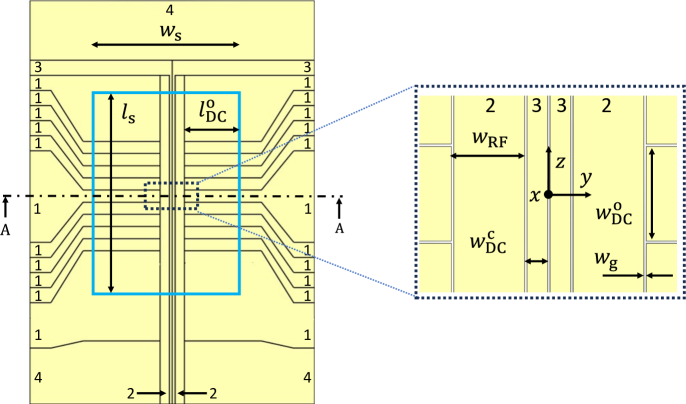
The height of 100 µm is selected to balance the trade-off between mitigating surface-induced heating [26, 27] and maintaining sufficient trapping depth for stable ion confinement. The trapping field is generated by the application of a RF (radio frequency) potential and DC (direct current) potentials to the corresponding electrodes. Given a RF amplitude of V and a RF frequency of MHz, we obtain a secular frequency of MHz and a trapping depth of 103.01 meV for a 172Yb+ ion. The relevant dimensions of the electrodes are detailed in Table 1.
| Symbol | Value | Dimension |
|---|---|---|
| 5 mm | length of the simulation region | |
| 2.4 mm | width of the simulation region | |
| 1 mm | length of the outer DC electrode | |
| 200 m | width of the outer DC electrode | |
| 150 m | width of the RF electrode | |
| 44.3 m | width of the center DC electrode | |
| 5 m | width of the gap between electrodes |
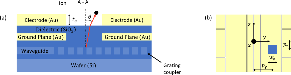
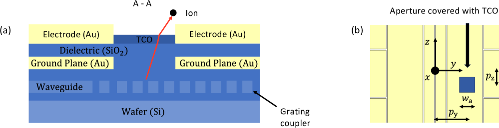
To integrate optical components into the surface trap, we adapted the layer stack-up from reference [12] in the design as depicted in figure 2. A waveguide layer with grating outcouplers is implemented beneath the electrodes. Light is coupled into this layer, guided, and subsequently coupled out vertically by grating outcouplers through apertures in the gold electrodes.
The discontinuity arising from the aperture can introduce a distortion of the trapping field. We investigate the distortion of the trapping RF field using FEM simulations with the commercial software COMSOL Multiphysics 5.6. All simulations utilize square-shaped apertures. The target ion position for a single ion is 100 m directly above the trap center. The ion’s position in the radial direction (in x-y plane), which is perpendicular to the trap axis, is determined by the minimum of the radial RF field in this plane, where . This position is influenced by the electrode geometry and is independent on the magnitude of the RF field. Due to the finite length of the trap, a residual RF field exists along the trap axis. This residual field scales with the magnitude of the applied RF field. Accordingly, in the following discussion, we consider distortions in the radial and axial directions separately. In the radial direction, we analyze the displacement of the minimum from the target ion position, while in the axial direction, we examine the residual RF field along the trap axis. To simplify the simulation of the trapping field, it is initially sufficient to consider the RF field at a fixed phase, which reduces the problem to an electrostatic analysis [28]. For the simulations presented in the following sections, we set V and keep all V unless otherwise stated.
3 Design constraints imposed by grating couplers
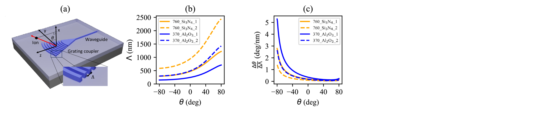
The grating couplers constrain the position and the geometry of the apertures in the trap electrodes. The light from the waveguide is coupled out at an angle by a grating coupler when the Bragg condition,
| (1) |
is satisfied, where is the effective refractive index of the grating, is the diffraction order, is the wavelength and is the period of the grating. Figure 3(a) illustrates the structure of a grating coupler. A backward grating coupler emits in the direction opposite to the propagation of the guided light, resulting in a negative diffraction angle , while a forward grating coupler diffracts the guided light with a positive diffraction angle . As illustrated in figures 3(b) and (c), the grating period decreases as transitions from positive to negative values, while the absolute angle-to-period sensitivity increases. Additionally, shorter wavelengths require smaller grating periods and exhibit higher angle-to-period sensitivity. Another consideration for trap design is that, backward grating couplers emit only first-order diffraction, while forward grating couplers can generate both first and higher-order diffracted beams. For instance, for a Si3N4 forward grating coupler with a thickness of 200 nm, the second-order beam is outcoupled if °. These higher order beams can cause unwanted stray light in the ion trap.
4 Results
In this section, we first discuss the RF field distortion resulting from a single aperture in different types of trap electrodes. Next, we examine how the position and geometry of an aperture, specifically in a RF electrode, affect this distortion. Following this, we investigate methods to reduce the distortion by utilizing symmetry and applying transparent conductive oxide materials. Throughout the discussion, the configuration without any aperture in the trap electrodes is treated as the reference configuration, providing a baseline to evaluate the effects of apertures on the RF field distortion.
4.1 Effect of a single aperture in the RF electrode, the center DC electrode, or the outer DC electrode
We begin by investigating the electric field distortion caused by a square-shaped aperture with width = 30 m positioned in either the RF electrode, center DC electrode, or outer DC electrode (figure 4). These positions correspond to outcoupling angles ranging from to , encompassing the range of angles demonstrated in previously reported ion traps with integrated waveguides and grating couplers [11, 14, 15, 16, 12, 13].
Shift of the RF field minimum in radial direction
The unperturbed radial RF electric field () in x-y plane for the reference configuration is illustrated in figure 5(a). When an aperture with a size
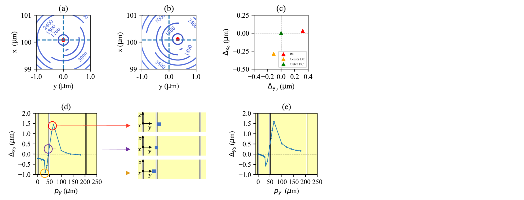
of = 30 m is present in the RF electrode, see figure 4(a), the radial electric field is shifted in x-y plane as illustrated in figure 5(b). The radial field minimum is displaced by 320 nm from the target ion position in y-direction and 30 nm in x-direction.
Figure 5(c) provides a summary of the minimum displacements in both x and y-directions for an aperture in the RF electrode, the center DC electrode, and the outer DC electrode. When the aperture is in the outer DC electrode, the minimum experiences a less significant displacement compared to the RF or the center DC electrode. When an aperture is located in the RF electrode, the minimum mainly shifts in positive y-direction. In contrast, when the aperture is placed in the center DC electrode, the displacement reverses its direction, and the shift in x-direction becomes more prominent.
We resolve the transition of the displacement as the aperture is moved from the RF electrode to the center DC electrode, depicted in figure 5 (d-e). The displacement reaches its absolute maximum when the aperture is located such that one side of the aperture coincides with the edge of the electrode. A zero displacement occurs when the aperture is positioned in the gap between electrodes due to a sign change in the displacement. As the aperture moves closer to the trap center, the displacement magnitude decreases. When the aperture is directly beneath the target ion position, the displacement magnitude in x-direction reaches a minimum of 200 nm, while in y-direction it vanishes due to the trap’s symmetry with respect to the z-axis.
Residual RF field on the trap axis
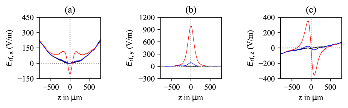
In the axial direction we evaluate the RF field along the trap axis as shown in figure 6. The residual RF field along the trap axis, resulting from the finite length of the trap, is shown by the black dashed line in figure 6. The x-component exhibits a weak parabolic increase, reaching an amplitude of 7.8 V/m and a gradient of 82 at z = 100 m. The amplitude of the y-component is zero along the entire trap axis due to the symmetry of the ion trap with respect to the z-axis. Meanwhile, the z-component maintains a constant gradient of approximately 65 across the trap axis, with its amplitude remaining zero at z = 0.
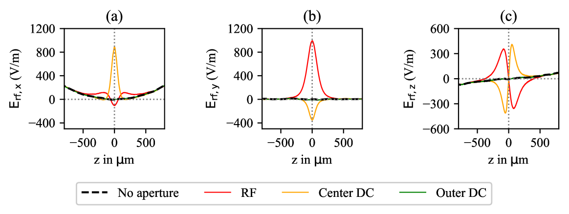
When an aperture is placed in the RF electrode, the residual RF field increases, particularly in the y- and z-components. The y-component (figure 6(b), red line) has a peak amplitude of 994 V/m at z = 0 and a gradient of 5.5 at the FWHM. The z-component (figure 6(c), red line) has a symmetric dispersive lineshape around z = 0 with a gradient of about 4.3 at z = 0. In contrast, an aperture in the center DC electrode mainly affects the x- and z-components. The x-component of the residual field (figure 6(a), orange line) has a peak amplitude of 887 V/m at z = 0 and a gradient of 8.5 at the FWHM. The z-component (figure 6(c), orange line) exhibits again a symmetric dispersive lineshape with a gradient of 7.8 at z = 0.
The differences in the radial components and at the target ion position (z = 0) explain the behavior of the displacement of the shown in figure 5(c). At the target ion position, for an aperture in the RF electrode dominates over , while for an aperture in the center DC electrode, becomes dominant. Additionally, both and switch signs depending on the aperture’s location. This explains why the minimum shifts positively, with the displacement more prominent in y-direction, when the aperture is in the RF electrode. For the case the aperture is in the center DC electrode, the displacement reverses direction, with x-direction shift becoming more pronounced.
To summarise the comparison of the three electrode types, placing the aperture in the outer DC electrode minimizes its effect on the trapping RF field due to the greater distance from the ion. However, this placement requires a large angle () of the outcoupled beam. According to the Bragg condition for backward grating couplers, larger outcoupling angles correspond to higher angle-to-period sensitivity, making them more sensitive to fabrication tolerances. For example, a 200 nm thick Si3N4 backward grating coupler at a wavelength of 760 nm exhibits an angle-to-period sensitivity of 1.4°/nm at °, see figure 3(b). Given a typical fabrication tolerance of 5 nm, this results in an angular deviation of . Combined with the increased distance from the target ion position, this deviation leads to significant beam misalignment of the laser beam to the ion. Using forward grating couplers alleviates this issue by having smaller angle-to-period sensitivity at the same angle, which are less sensitive to fabrication tolerances. However, forward grating couplers operated at large angles generate higher-order beams, as shown in figure 3. These unintended beams contribute to stray light and optical cross-talk, introducing errors that degrade the performance of atomic clocks and quantum logic operations. Although the apertures in the center DC and RF electrodes displace the ion in opposing directions due to the sign change and the varying dominance of distorted RF field components, their effects on the trapping field are comparable. Therefore, in the subsequent sections, we focus on the aperture in the RF electrode.
4.2 Effect of aperture position and geometry
4.2.1 Effect of aperture position
In this section, we examine how the field distortion scales with the position of the aperture in the RF electrode. We first vary the position of an aperture in z-direction
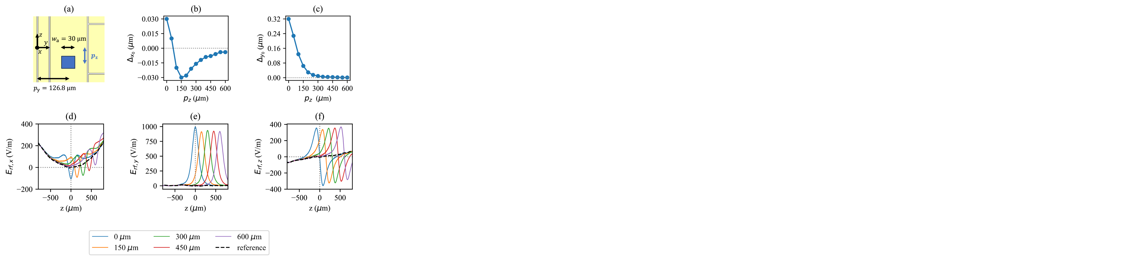
in the RF electrode while keeping = 30 m and = 126.8 m (centered in the RF electrode), as shown in figure 7. Figures 7(b) and (c) present the impact on the displacement of the minimum in x-y plane by varying from 0 m to 600 m.
The displacement of the minimum in x-direction ()
shifts from positive to negative as increases from 0 to 150 m, with the displacement vanishing at = 75 m. As the aperture is placed farther from the trap center, the displacement approaches zero. In contrast, the displacement in y-direction () follows a monotonic trend, decreasing steadily and approaching zero as increases.
The analysis along the trap axis (figures 7(d)-(f)) demonstrates that the RF field maintains its characteristic peak shapes similar to that shown by the red line in figure 6 while undergoing a spatial shift that corresponds to the aperture’s position. When the aperture is moved farther away from the trap center, the amplitudes and gradients of the RF field at the target ion position converge to the case without any aperture (black dashed line), since the influence of the aperture on the RF field at the target ion position decreases.
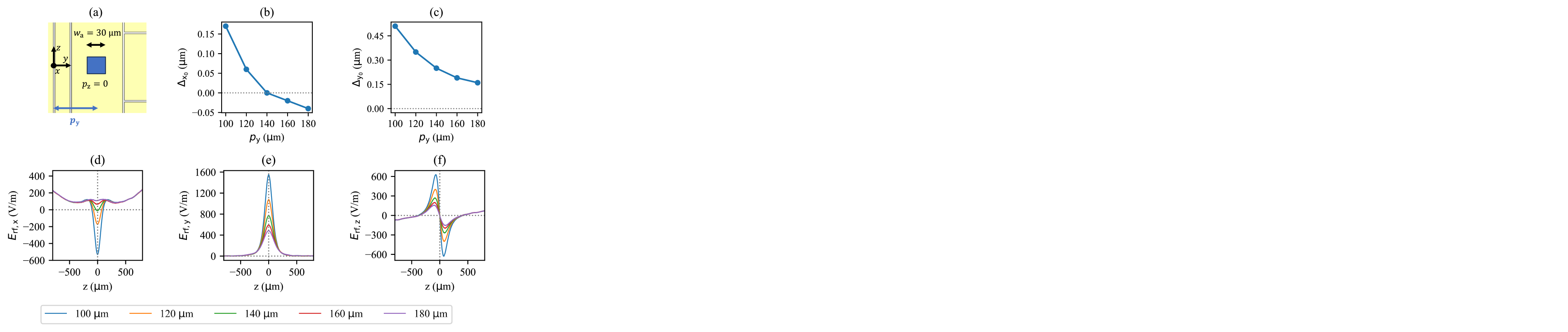
We then vary the position of an aperture in y-direction () in the RF electrode while keeping = 30 m and = 0 m (on the y-axis), as shown in figure 8. Figures 8(b) and (c) illustrate the effect on the displacement of the minimum in x-y plane by varying from 100 m to 180 m. The displacement of the minimum in x-direction () crosses from positive to negative as increases, with the displacement vanishing at = 140 m, while the displacement in y-direction () follows a monotonic downward trend, approaching zero as increases. Along the trap axis, as shown in figures 8(d)-(f), the peaks in the x- and y-components of the residual field remain centered at z = 0 and increase in magnitude as decreases. At = 100 m, attains an amplitude of approximately 500 V/m at z = 0 with a gradient of 5.2 at the FWHM, while achieves a higher amplitude of approximately 1500 V/m at z = 0 with a steeper gradient of 9.7 at the FWHM. The z-component
maintains its dispersive lineshape with a gradient at increasing significantly as decreases, reaching 9.1 at .
To summarize the effect of the aperture position, simulations indicate that placing the aperture farther from the trap center reduces RF field distortion at the target ion position, as expected. However, this geometric relationship creates a trade-off: greater distances require larger outcoupling angles, which in turn demand wider apertures.
4.2.2 Effect of aperture size
The required aperture size for the outcoupled beam depends on the ion height, the angle of the outcoupled beam, the required beam waist at the target ion position and the fabrication tolerances. The ion traps with integrated waveguides and grating couplers shown so far in reference [11, 14, 15, 16, 12, 13] have aperture sizes ranging from 10 m to 35 m, with ion heights varying from 20 m to 55 m. In our study, due to our greater ion height of 100 m, we examine RF field distortion by varying aperture width across a broader range from 10 m to 100 m while maintaining a fixed position in the RF electrode, as
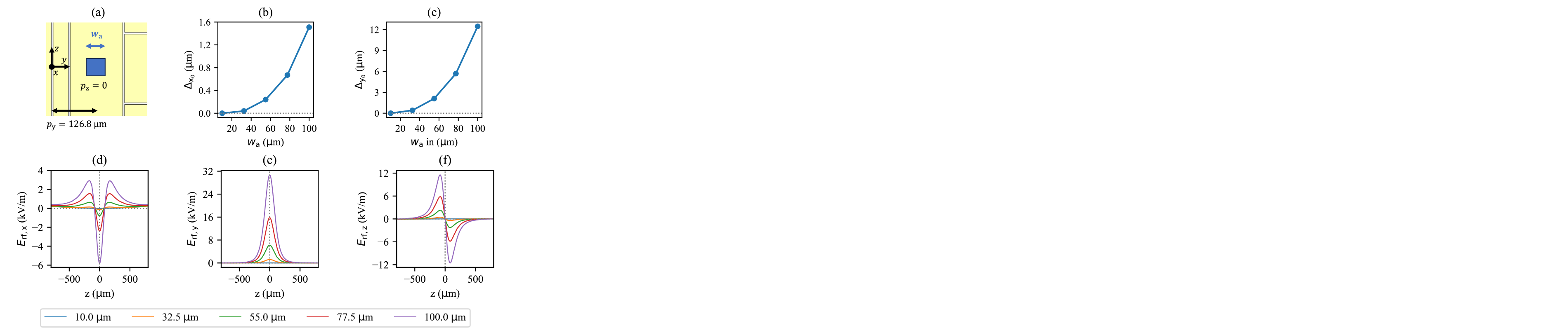
shown in figure 9. Increasing the aperture size from 10 m to 100 m causes a displacement of the minimum in x-y plane by up to 1.6 m in x-direction and up to 12 m in y-direction. Along the trap axis, the peaks of the x- and y-components of the residual field remain centered at z = 0 and become significantly deeper as increases. The x-component reaches an amplitude of approximately 6 kV/m at z = 0 with a strong gradient of 64.2 at the FWHM, while the y-component reaches about 30 kV/m at z = 0 with a gradient of 163.3 at the FWHM. The z-component maintains its characteristic dispersive lineshape with the gradient at z = 0 increasing significantly as increases, reaching 139 for = 100 m.
In comparison to variations in location, altering the size of the aperture has a more pronounced effect on the electric field distortion. A larger distance of the aperture from the trap center reduces distortion but requires a larger aperture, which in turn introduces additional distortion. Therefore, a careful balance must be struck between the distance and the size of the aperture.
4.2.3 Effect of electrode thickness
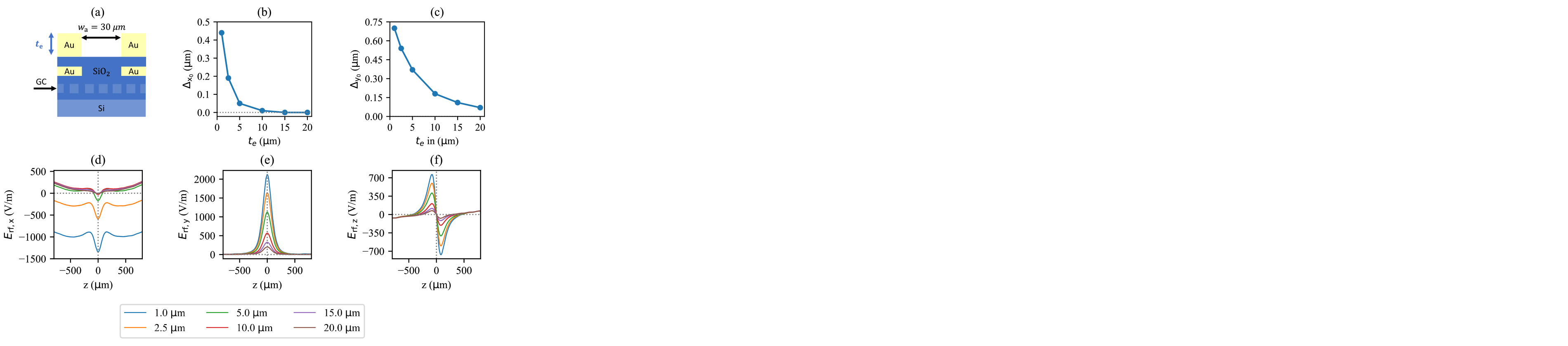
Next, we study the effect of the electrode thickness on the field distortion as presented in figure 10. Our results demonstrate that increasing electrode thickness reduces both the displacement of the minimum in x-y plane and the residual RF field along the trap axis. This improvement is due to the reduction of the edge effects. Edge effects arise when the geometry of the electrode, such as sharp edges or boundaries, introduces non-uniformities in the electric field, especially near the edges. The aperture in a thinner electrode has a more pronounced field distortion at its edges, because the field lines are less confined and can spread outward more easily, leading to larger variations in the trapping field. This behavior is similar to that seen in larger capacitors, where the influence of edge effects is diminished as the length of the capacitor (or in our case, the thickness of the electrode) increases.
4.3 Effect of symmetry
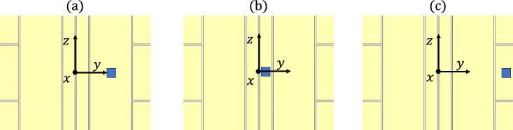
When a single aperture is positioned off the symmetry axes (either y or z), as illustrated in figure 11(a), the minimum in x-y plane is displaced from its target position. The asymmetry also leads to residual RF field amplitude and gradients in all three components at the target ion position.
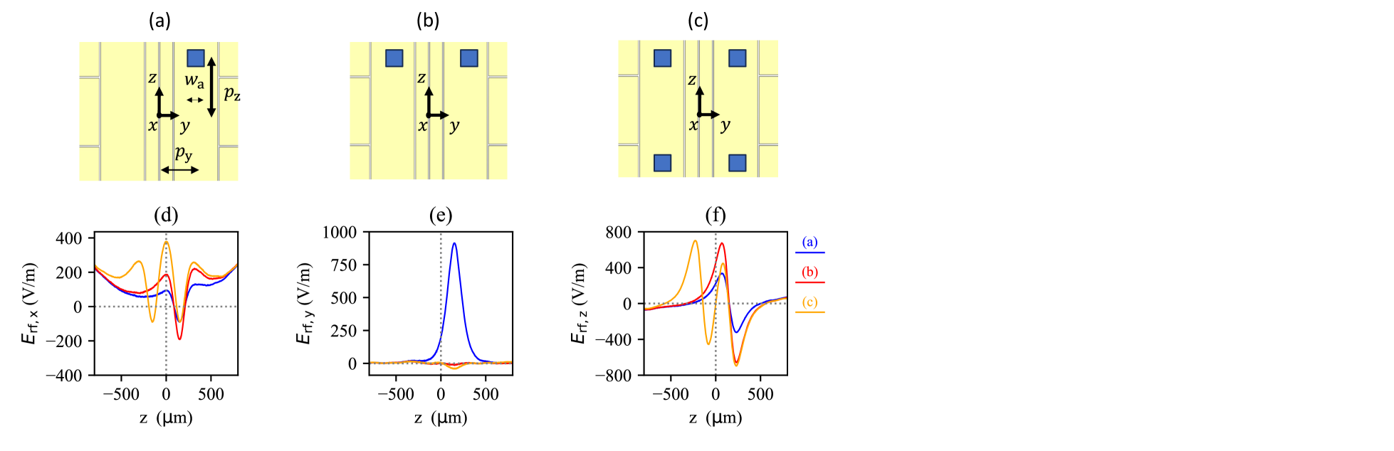
To address the displacement in the radial direction, we first introduce an additional aperture placed symmetrically with respect to the z-axis, as shown in figure 11(b). The analysis along the trap axis (figures 11(d)-(f), red line) demonstrates that this z-symmetry cancels the y-component of the RF field along the entire trap axis, while simultaneously enhancing the peaks of the x- and z-components.
Next, to compensate the residual RF amplitude in the z-component at the target ion position (z = 0), we introduce two additional apertures to create y-symmetry, as depicted in figure 11(c). The analysis along the trap axis (figures 11(d)-(f), orange line) shows that while vanishes at z = 0 as expected, the introduction of the extra apertures creates additional peaks in the field. Furthermore, the x-component exhibits a more complex lineshape with additional peaks and a non-vanishing field amplitude at z = 0. Since surface ion traps are inherently two-dimensional, exploiting x-symmetry for further compensation is not feasible, meaning that the x-component cannot be fully mitigated in this configuration.
4.4 Effect of using transparent conductive oxide coating
Transparent conductive oxides (TCOs) have the advantage of being both conductive and transparent [29], which can be applied as thin film coatings to cover the aperture, shown in figure 12. These thin films are electrically connected to the electrodes, thus sharing their potential while allowing outcoupled light to pass through. In addition, the TCO covers the dielectric area that could potentially charge up due to laser-induced charging [30, 31] and detrimentally affect the electric field at the ion location. However, a trade-off between conductivity and transparency typically limits the thickness of TCO to about a few tens of nanometers [32], which is significantly thinner than the gold layers used for the surface electrode. One commonly used TCO material is Indium Tin Oxide (ITO), which has a conductivity on the order of S/m [29, 32, 33, 34, 35] and typically has a thickness of approximately 50 nm. In all following simulations, the thickness of TCO () is set to 50 nm.
4.4.1 Effect of modified topography of the electrode
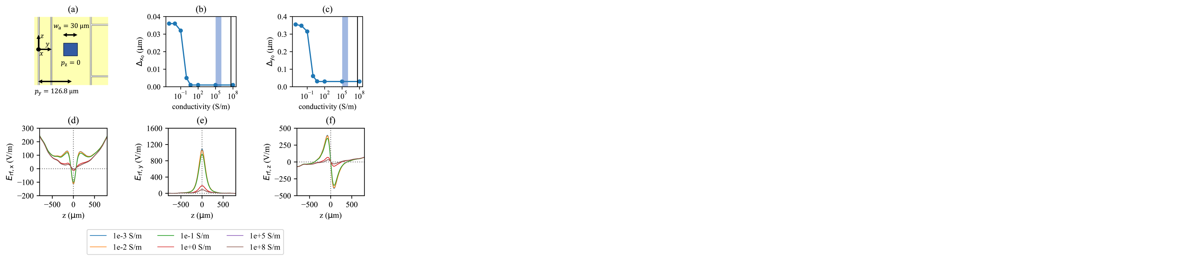
To account for the thickness difference in the trap electrode at the outcoupling aperture, we initially assume an idealized TCO layer with a conductivity equivalent to gold (4.5 × S/m), thereby ensuring that the layer shares the same electrical potential as the gold electrode.
The simulation results (see figure 13) indicate that, although the RF field along the trap axis are substantially reduced when TCO is applied (blue line) in comparison to the case without TCO (red line), a small residual RF field remains in comparison to the reference configuration (black). In the radial direction, the minimum in x-y plane exhibits a residual displacement of approximately 30 nm in y-direction and no displacement in x-direction when the aperture is covered with TCO. Although the displacements are significantly smaller than in the case without the TCO coating (30 nm in x-direction and 320 nm in y-direction as shown in figure 5(c)), they do not vanish entirely.
4.4.2 Effect of varying the conductivity of TCO
The conductivity of TCO is strongly influenced by its material composition and manufacturing process. To assess the effect of the TCO conductivity on RF field distortion, we vary the conductivity of the TCO layer and model the RF field by taking into account the current flow through both the gold electrode and the TCO. This simulation cannot be treated statically, therefore we use the electric current module in COMSOL. A voltage source with a frequency of 16 MHz and an amplitude of 100 V is applied to the RF electrodes. All other DC electrodes are grounded. This method captures both the phase and potential distortions in the electrode, from which the RF field at the target ion position is calculated.
In x-y plane, the displacement of the minimum decreases in both x- and y-directions as the conductivity of TCO increases, as shown in figure 14. The blue band indicates the region of typical conductivities of ITO and the black line indicates the conductivity of gold. When the conductivity of TCO matches that of gold ( S/m), the displacement in x-direction vanishes, while a residual displacement of 30 nm remains in y-direction, which is consistent with results from the electrostatic simulation in Section 4.4.1. A similar trend is observed in the axial direction as well. As the conductivity of the TCO increases to match that of gold, the RF field along the trap axis converges to the results shown by the blue line in figure 13 in Section 4.4.1.
4.4.3 Effect of the RF phase shift
The aperture in the RF electrode not only distorts the potential of the electrode, but also introduces a phase delay due to the differences in conductivity and thickness between gold and TCO. Such phase difference between the two RF electrodes can cause a non-zero minimum, resulting in excess micromotion that can not be compensated [21].
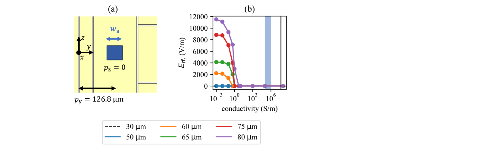
Figure 15 shows the residual amplitude of at its minimum as a function of the TCO conductivity for varying aperture widths . The residual amplitude exhibits distinct behavior across different conductivity regimes. At low conductivities (below 1 S/m) with 50 m, exhibits a significant residual amplitude at its minimum. This arises from the mismatch in conductivity and thickness between the gold and TCO coatings, which induces a phase delay in the RF electrode and results in a non-vanishing field amplitude at the minimum. As the conductivity decreases further to S/m, where the aperture effectively behaves as if it had no TCO coating, the residual amplitude converges to a maximum. This indicates that the cut-through in the RF electrode created by the aperture introduces strong phase distortions (for 50 m), resulting in a residual minimum that can not be fully compensated. Conversely, increasing TCO conductivity reduces the residual field amplitude. When the conductivity reaches the value of commonly used ITO or matches that of gold, the residual amplitude vanishes for all aperture widths. This indicates that the phase delay due to thickness differences between the TCO and gold is negligible.
To summarize the effect of TCO, our findings indicate that the effect of the conductivity of the TCO on the RF field can be neglected over a large range from 10 S/m to S/m. This can be explained by modeling the TCO covering the aperture and the gold on its sides as impedances connected in parallel. In this model, the gold provides a highly conductive path with negligible resistance compared to the TCO. As the gold dominates the total impedance, the TCO’s conductivity has minimal impact on RF field if it is S/m. The conductivity and the thickness of the commonly used ITO layers are adequate to mitigate significant RF field distortion without introducing a phase shift in the RF electrode. However, the topography of the surface electrodes with apertures prevents a complete elimination of the RF field distortion.
5 Conclusion and Outlook
In this paper, we present a comprehensive analysis of the effects on the trapping field of a photonic-integrated surface ion trap caused by apertures for vertically outcoupled laser beams from waveguides. We find that placing apertures in the outer DC electrode is the optimal strategy to avoid significant trapping field distortion. However, this requires larger outcoupling angles. For backward grating couplers, larger angles necessitate smaller grating periods and have higher angle-to-period sensitivity, making them highly sensitive to fabrication tolerances. In the case of forward grating couplers, for larger angles higher-order diffraction are coupled out. These effects become more pronounced at shorter wavelengths. For instance, given a typical fabrication tolerance of 5 nm, a 120 nm thick Al2O3 backward grating coupler at a wavelength of 370 nm exhibits an angle-to-period sensitivity of 2.7°/nm at °, leading to an angular deviation of approximately 13.5°. Such a grating coupler requires a feature size of approximately 70 nm, which is critical for foundries [36].
When the aperture is located in the RF electrode, a trade-off emerges between the distance from the trap center and the size of the aperture. As the distance increases, the distortion of the trapping field leads to a smaller displacement of the minimum. For distances from m to m in the RF electrode, the displacement reduces from m to 150 nm in the y-direction and m to 50 nm in the x-direction. For a shift of the aperture position in the RF electrode in the z-direction, a similar behavior is observed with a displacement on the same scale. However, the distortion and the resulting displacement also depend on the aperture size. While the displacement is m for a square-shaped aperture of width m at = 126.8 m and = 0 m, for a larger aperture with m at the same position the ion is displaced by m and m. This large displacement is due to the highly distorted field, with the y-component exhibiting a peak amplitude of 30 kV/m and a gradient of 164 V/mm2 at the target ion position. Importantly, the aperture should not be placed at the edge of the gap between the center DC and RF electrodes, as this results in a larger ion displacement of 1.5 m in both directions compared to when the aperture is fully surrounded by the metal electrode. When the aperture is positioned in the center DC electrode, the ion displacement can be minimized to 150 nm and can be zeroed by placing the aperture directly at the trap center.
With a fixed aperture width, increasing the thickness of the electrode from 1 m to 20 m can reduce field distortions by two orders of magnitude, due to the reduction of the edge effect. However, care must be taken to ensure that the electrode does not obstruct the outcoupled laser beam, unless a technique is developed to shape the metal layer of the electrode at the angle of the outcoupled beam.
Arranging apertures symmetrically provides an effective strategy for compensating the displacement of the minimum and the phase difference between the RF electrodes. Nevertheless, this approach introduces stronger residual RF fields along the trap axis, if additional apertures are required or if the aperture size must be increased to maintain symmetry. Independent of the presence of an aperture in an electrode, it is not possible to fully compensate the out-of-plane component (x) of the RF field at the target ion position due to the inherently two-dimensional geometry of planar surface traps.
The application of TCO coatings on apertures significantly reduces the potential and phase distortions on the electrodes, thereby strongly reducing RF field distortions at the target ion position, e.g. from V/m to V/m. Only small residual RF field components remain due to the topography of the modified surface. Future technological developments could focus on leveling the topography of surface traps to reach a flat surface with TCO coating.
References
References
- [1] Bruzewicz C D, Chiaverini J, McConnell R and Sage J M 2019 Trapped-ion quantum computing: Progress and challenges Appl. Phys. Rev. 6 021314
- [2] Blatt R and Roos C F 2012 Quantum simulations with trapped ions Nature Physics 8 277–284
- [3] Degen C L, Reinhard F and Cappellaro P 2017 Quantum sensing Rev. Mod. Phys. 89(3) 035002 URL https://link.aps.org/doi/10.1103/RevModPhys.89.035002
- [4] Giovannetti V, Lloyd S and Maccone L 2004 Quantum-enhanced measurements: Beating the standard quantum limit Science 306 1330–1336 (Preprint arXiv:https://www.science.org/doi/pdf/10.1126/science.1104149) URL https://www.science.org/doi/abs/10.1126/science.1104149
- [5] Moses S A, Baldwin C H, Allman M S, Ancona R, Ascarrunz L, Barnes C, Bartolotta J, Bjork B, Blanchard P, Bohn M, Bohnet J G, Brown N C, Burdick N Q, Burton W C, Campbell S L, Campora J P, Carron C, Chambers J, Chan J W, Chen Y H, Chernoguzov A, Chertkov E, Colina J, Curtis J P, Daniel R, DeCross M, Deen D, Delaney C, Dreiling J M, Ertsgaard C T, Esposito J, Estey B, Fabrikant M, Figgatt C, Foltz C, Foss-Feig M, Francois D, Gaebler J P, Gatterman T M, Gilbreth C N, Giles J, Glynn E, Hall A, Hankin A M, Hansen A, Hayes D, Higashi B, Hoffman I M, Horning B, Hout J J, Jacobs R, Johansen J, Jones L, Karcz J, Klein T, Lauria P, Lee P, Liefer D, Lu S T, Lucchetti D, Lytle C, Malm A, Matheny M, Mathewson B, Mayer K, Miller D B, Mills M, Neyenhuis B, Nugent L, Olson S, Parks J, Price G N, Price Z, Pugh M, Ransford A, Reed A P, Roman C, Rowe M, Ryan-Anderson C, Sanders S, Sedlacek J, Shevchuk P, Siegfried P, Skripka T, Spaun B, Sprenkle R T, Stutz R P, Swallows M, Tobey R I, Tran A, Tran T, Vogt E, Volin C, Walker J, Zolot A M and Pino J M 2023 A race-track trapped-ion quantum processor Phys. Rev. X 13(4) 041052 URL https://link.aps.org/doi/10.1103/PhysRevX.13.041052
- [6] Pogorelov I, Feldker T, Marciniak C D, Postler L, Jacob G, Krieglsteiner O, Podlesnic V, Meth M, Negnevitsky V, Stadler M, Höfer B, Wächter C, Lakhmanskiy K, Blatt R, Schindler P and Monz T 2021 Compact ion-trap quantum computing demonstrator PRX Quantum 2(2) 020343 URL https://link.aps.org/doi/10.1103/PRXQuantum.2.020343
- [7] Zesar A, Wahl J, Castro S C, Schüppert K, Colombe Y, Auchter S, Glantschnig M, Rössler C, Lamprecht B, Hurdax P, Schmauser M, Valentini M, Schindler P, Monz T, Gordillo O J, Melloni A and Krenn J 2024 Industrial ion trap chips with integrated optics The 25th European Conference on Integrated Optics ed Witzens J, Poon J, Zimmermann L and Freude W (Cham: Springer Nature Switzerland) pp 222–229 ISBN 978-3-031-63378-2
- [8] Sotirova A S, Sun B, Leppard J D et al 2024 Low cross-talk optical addressing of trapped-ion qubits using a novel integrated photonic chip Light: Science & Applications 13 199
- [9] Day M L, Choonee K, Chaboyer Z, Gross S, Withford M J, Sinclair A G and Marshall G D A micro-optical module for multi-wavelength addressing of trapped ions 6 024007 URL https://dx.doi.org/10.1088/2058-9565/abdf38
- [10] Ghadimi M, Blüms V, Norton B G and et al 2017 Scalable ion–photon quantum interface based on integrated diffractive mirrors npj Quantum Information 3 4
- [11] Mehta K K, Bruzewicz C D, McConnell R, Ram R J, Sage J M and Chiaverini J 2016 Integrated optical addressing of an ion qubit Nature Nanotechnology 11 1066–1070
- [12] Mehta K K, Zhang C, Malinowski M, Nguyen T L, Stadler M and Home J P 2020 Integrated optical multi-ion quantum logic Nature 586 533–537
- [13] Mordini C, Vasquez A R, Motohashi Y, Müller M, Malinowski M, Zhang C, Mehta K K, Kienzler D and Home J P 2024 Multi-zone trapped-ion qubit control in an integrated photonics qccd device (Preprint arXiv:2401.18056) URL https://arxiv.org/abs/2401.18056
- [14] Niffenegger R J, Stuart J, Sorace-Agaskar C, Kharas D, Bramhavar S, Bruzewicz C D, Loh W, Maxson R T, McConnell R, Reens D, West G N, Sage J M and Chiaverini J 2020 Integrated multi-wavelength control of an ion qubit Nature 586 538–542
- [15] Ivory M, Setzer W J, Karl N, McGuinness H, DeRose C, Blain M, Stick D, Gehl M and Parazzoli L P 2021 Integrated optical addressing of a trapped ytterbium ion Phys. Rev. X 11(4) 041033 URL https://link.aps.org/doi/10.1103/PhysRevX.11.041033
- [16] Kwon J, Setzer W J, Gehl M, Karl N, Van Der Wall J, Law R, Blain M G, Stick D and McGuinness H J 2024 Multi-site integrated optical addressing of trapped ions Nature Communications 15 3709
- [17] West G N, Loh W, Kharas D, Sorace-Agaskar C, Mehta K K, Sage J, Chiaverini J and Ram R J 2019 Low-loss integrated photonics for the blue and ultraviolet regime APL Photonics 4 026101 URL https://doi.org/10.1063/1.5052502
- [18] Hendriks W A P M, Dijkstra M, Mardani S, Hegeman I and Garcia-Blanco S M 2023 Low-loss photonic integrated circuits for UV applications Integrated Optics: Devices, Materials, and Technologies XXVII vol 12424 ed García-Blanco S M and Cheben P International Society for Optics and Photonics (SPIE) p 1242402 URL https://doi.org/10.1117/12.2657143
- [19] Beck G J, Home J P and Mehta K K 2024 Grating design methodology for tailored free-space beam-forming Journal of Lightwave Technology 42 4939–4951
- [20] Wineland D J, Monroe C R, Itano W M, Leibfried D, King B E and Meekhof D M 1997 Experimental issues in coherent quantum-state manipulation of trapped atomic ions Journal of Research of the National Institute of Standards and Technology 103 259 – 328 URL https://api.semanticscholar.org/CorpusID:210657
- [21] Berkeland D J, Miller J D, Bergquist J C, Itano W M and Wineland D J Minimization of ion micromotion in a Paul trap 83 5025–5033 ISSN 0021-8979 (Preprint arXiv:https://pubs.aip.org/aip/jap/article-pdf/83/10/5025/18699946/5025_1_online.pdf) URL https://doi.org/10.1063/1.367318
- [22] Kalincev D, Dreissen L S, Kulosa A P, Yeh C H, Fürst H A and Mehlstäubler T E 2021 Motional heating of spatially extended ion crystals Quantum Science and Technology 6 034003 URL https://dx.doi.org/10.1088/2058-9565/abee99
- [23] Blakestad R B, Ospelkaus C, VanDevender A P, Amini J M, Britton J, Leibfried D and Wineland D J 2009 High-fidelity transport of trapped-ion qubits through an -junction trap array Phys. Rev. Lett. 102(15) 153002 URL https://link.aps.org/doi/10.1103/PhysRevLett.102.153002
- [24] Keller J, Burgermeister T, Kalincev D, Didier A, Kulosa A P, Nordmann T, Kiethe J and Mehlstäubler T E 2019 Controlling systematic frequency uncertainties at the level in linear coulomb crystals Phys. Rev. A 99(1) 013405 URL https://link.aps.org/doi/10.1103/PhysRevA.99.013405
- [25] Allcock D T C, Sherman J A, Stacey D N, Burrell A H, Curtis M J, Imreh G, Linke N M, Szwer D J, Webster S C, Steane A M and Lucas D M 2010 Implementation of a symmetric surface-electrode ion trap with field compensation using a modulated raman effect New Journal of Physics 12 053026 URL https://dx.doi.org/10.1088/1367-2630/12/5/053026
- [26] Epstein R J, Seidelin S, Leibfried D, Wesenberg J H, Bollinger J J, Amini J M, Blakestad R B, Britton J, Home J P, Itano W M, Jost J D, Knill E, Langer C, Ozeri R, Shiga N and Wineland D J 2007 Simplified motional heating rate measurements of trapped ions Phys. Rev. A 76(3) 033411 URL https://link.aps.org/doi/10.1103/PhysRevA.76.033411
- [27] Deslauriers L, Olmschenk S, Stick D, Hensinger W K, Sterk J and Monroe C 2006 Scaling and suppression of anomalous heating in ion traps Phys. Rev. Lett. 97(10) 103007 URL https://link.aps.org/doi/10.1103/PhysRevLett.97.103007
- [28] Herschbach N, Pyka K, Keller J and Mehlstäubler T E 2012 Linear paul trap design for an optical clock with coulomb crystals Applied Physics B 107 891–906 ISSN 1432-0649 URL https://doi.org/10.1007/s00340-011-4790-y
- [29] Stadler A 2012 Transparent conducting oxides—an up-to-date overview Materials 5 661–683 ISSN 1996-1944 URL https://www.mdpi.com/1996-1944/5/4/661
- [30] Wang S X, Hao Low G, Lachenmyer N S, Ge Y, Herskind P F and Chuang I L 2011 Laser-induced charging of microfabricated ion traps Journal of Applied Physics 110 104901 ISSN 0021-8979 (Preprint arXiv:https://pubs.aip.org/aip/jap/article-pdf/doi/10.1063/1.3662118/15083503/104901_1_online.pdf) URL https://doi.org/10.1063/1.3662118
- [31] Ong F R, Schüppert K, Jobez P, Teller M, Ames B, Fioretto D A, Friebe K, Lee M, Colombe Y, Blatt R and Northup T E 2020 Probing surface charge densities on optical fibers with a trapped ion New Journal of Physics 22 063018 URL https://dx.doi.org/10.1088/1367-2630/ab8af9
- [32] Jansson E, Scheuer V, Jordan E, Kostourou K and Mehlstäubler T E 2024 Indium tin oxide combined with anti-reflective coatings with high transmittance for wavelengths ¡ 400 nm (Preprint arXiv:2411.10361) URL https://arxiv.org/abs/2411.10361
- [33] Kim C, Park J W, Kim J, Hong S J and Lee M J 2017 A highly efficient indium tin oxide nanoparticles (ito-nps) transparent heater based on solution-process optimized with oxygen vacancy control Journal of Alloys and Compounds 726 712–719
- [34] Kim D, Han Y, Cho J S and Koh S K 2000 Low temperature deposition of ito thin films by ion beam sputtering Thin Solid Films 377 81–86
- [35] Hao L, Diao X, Xu H, Gu B and Wang T 2008 Thickness dependence of structural, electrical and optical properties of indium tin oxide (ito) films deposited on pet substrates Applied surface science 254 3504–3508
- [36] Siew S Y, Li B, Gao F, Zheng H Y, Zhang W, Guo P, Xie S W, Song A, Dong B, Luo L W, Li C, Luo X and Lo G Q 2021 Review of silicon photonics technology and platform development J. Lightwave Technol. 39 4374–4389 URL https://opg.optica.org/jlt/abstract.cfm?URI=jlt-39-13-4374