Ultrafast decoupling of polarization and strain in ferroelectric
Abstract
A fundamental understanding of the interplay between lattice structure, polarization and electrons is pivotal to the optical control of ferroelectrics. The interaction between light and matter enables the remote and wireless control of the ferroelectric polarization on the picosecond timescale, while inducing strain, i.e., lattice deformation. At equilibrium, the ferroelectric polarization is proportional to the strain, and is typically assumed to be so also out of equilibrium. Decoupling the polarization from the strain would remove the constraint of sample design and provide an effective knob to manipulate the polarization by light. Here, upon an above-bandgap laser excitation of the prototypical ferroelectric BaTiO3, we induce and measure an ultrafast decoupling between polarization and strain that begins within , by softening Ti-O bonds via charge transfer, and lasts for several tens of picoseconds. We show that the ferroelectric polarization out of equilibrium is mainly determined by photoexcited electrons, instead of the strain. This excited state could serve as a starting point to achieve stable and reversible polarization switching via THz light. Our results demonstrate a light-induced transient and reversible control of the ferroelectric polarization and offer a pathway to control by light both electric and magnetic degrees of freedom in multiferroics.
Ferroelectric materials are characterized by many properties, including piezoelectricity and pyroelectricity, besides ferroelectricity, which make them attractive for a wide range of applications, such as nonvolatile memories, transistors, sensors, and actuators[1, 2]. The key property of a ferroelectric material is the ability to switch its spontaneous polarization in response to an external electric field. This is typically achieved by a static or pulsed electric field with the consequent limitations given by the need for complex circuitry and switching times of hundreds of picoseconds to nanoseconds[3]. These challenges can be overcome by optical control of the ferroelectric polarization. Light-matter interaction enables remote and wireless control of the ferroelectric polarization on the picosecond timescale[3]. Moreover, since all ferroelectrics are also piezoelectrics, the ferroelectric polarization is strongly coupled to the strain, i.e., the lattice deformation[4]. Optical control of polarization and strain has been achieved in several cases. For example, in multilayers of ferroelectric and electrode thin films, an optical laser was used to excite the metal (or semiconductor) layer and indirectly the ferroelectric material, leading to a transient modification of the strain[5, 6, 7, 8], or the polarization by charge redistribution at the interface[9]. In other studies, light was absorbed directly by the ferroelectric material, inducing changes in the spontaneous polarization[10, 11] or lattice strain in clamped[12, 13, 14, 15, 16, 17, 18] or freestanding[19] ferroelectric thin films. THz light was employed to rotate[20] or even transiently reverse the orientation of the spontaneous polarization [21]. In all these studies so far, either the polarization or the strain was measured, and a direct proportionality between spontaneous polarization and strain was typically assumed[22]. This proportionality is based on the piezoelectric effect, which is well captured by the Landau-Ginzburg-Devonshire theory when the lattice distortion is along the polarization axis[23]. While this assumption is valid under equilibrium conditions, as demonstrated experimentally, e.g. in Refs.[24, 25], it may not hold under out-of-equilibrium conditions following light-matter interaction. Decoupling the polarization from the strain would remove the constraint of sample design to achieve specific properties [24, 26], and, at the same time, would provide a more effective and ultrafast knob to manipulate the polarization by light.
To explore this scenario, we probe the out-of-plane strain and the spontaneous polarization of the prototypical ferroelectric BaTiO3 upon above-bandgap absorption of ultrashort UV light pulses (Figure 1a). A fundamental understanding of the relationship between strain and ferroelectric polarization out of equilibrium requires their investigation on their natural timescale encompassing to several tens of . We employ a combination of time-resolved X-ray diffraction (tr-XRD), time-resolved optical second harmonic generation (tr-SHG), and time-resolved optical reflectivity (tr-refl) to obtain the magnitudes and the separate dynamics of the out-of-plane lattice parameter, the spontaneous polarization, and the photoexcited carrier density, respectively[27], with a time resolution of . In this paper, we will show the mechanisms that govern the structure and polarization changes in a ferroelectric material and their complex relationship out of equilibrium in the presence of photoexcited electrons and lattice deformation. In particular, since the strain wave propagates at the speed of sound, whereas electronic interactions are much faster, we induce and measure an ultrafast decoupling between polarization and strain, which we assign to the photoexcited electrons. First, we present the lattice response to the absorption of UV laser pulses and the corresponding data modeling. Next, we present tr-SHG and tr-refl data. Finally, we bring together all the results and discuss the underlying physical mechanisms in the context of hitherto known phenomena taking place in ferroelectric materials.
Results
Photoinduced structural dynamics
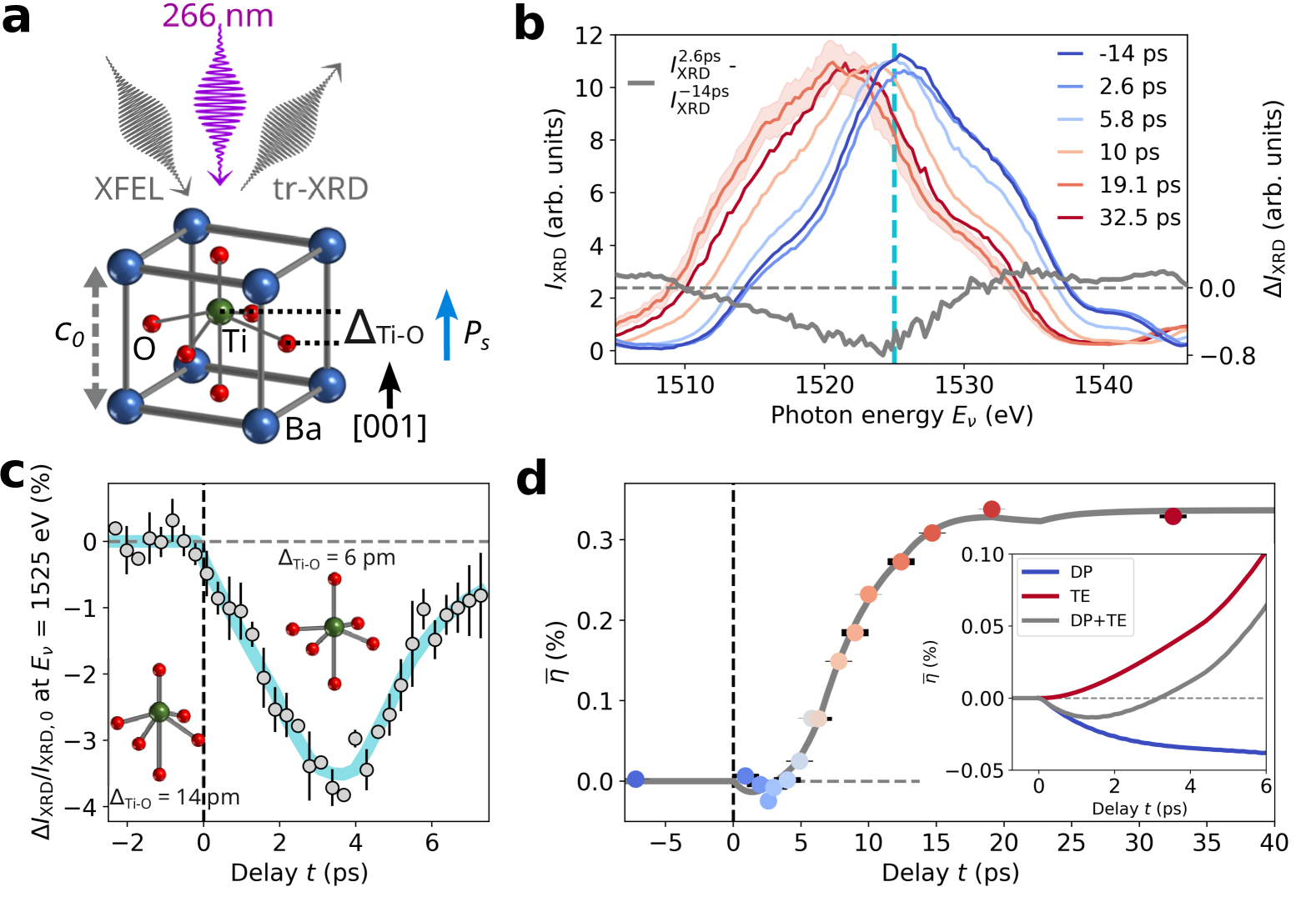
Our sample consists of a coherently strained, monodomain BaTiO3 (BTO) thin film, grown on a GdScO3 (GSO) substrate, with a SrRuO3 (SRO) bottom electrode sandwiched in between (see Methods). Under a compressive strain of imposed by the substrate, the BTO film shows an out-of-plane ferroelectric polarization pointing toward the sample surface (Figure 1a). The sample is excited above the BTO band gap [28] using laser pulses at an incident pump laser fluence of . Time-resolved X-ray diffraction of the (001) Bragg reflection is employed to probe the lattice response of our ferroelectric thin film along the out-of-plane direction. The lattice deformations along the in-plane directions on the picosecond timescale are negligible, given the large ratio between photoexcited area ( ) and BTO film thickness .
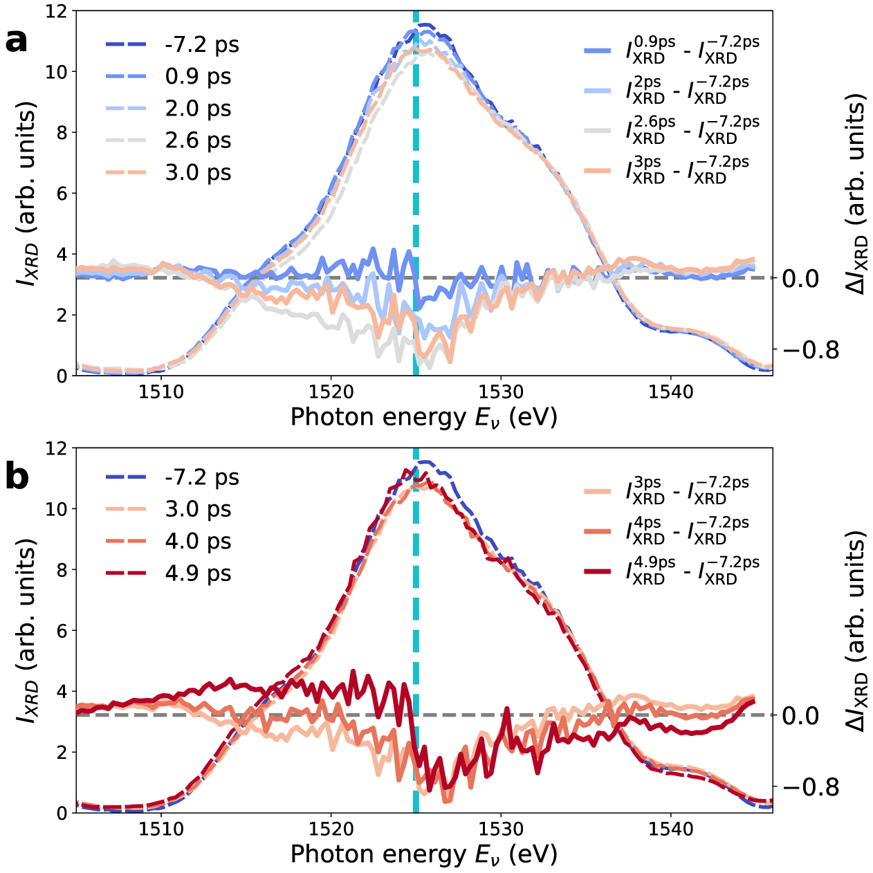
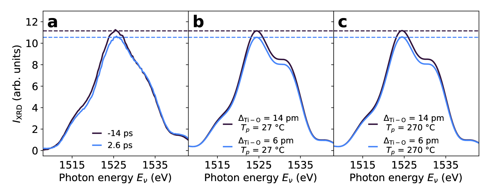
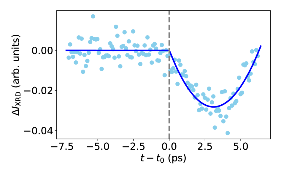
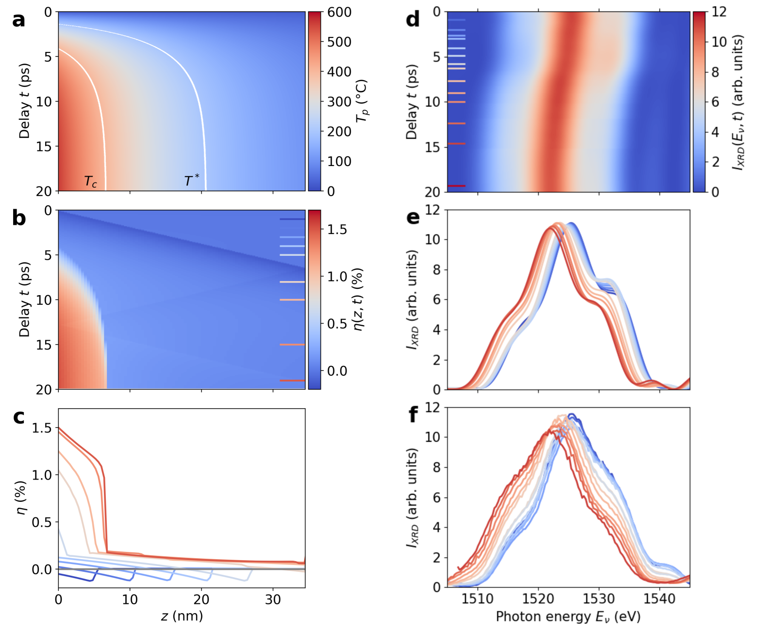
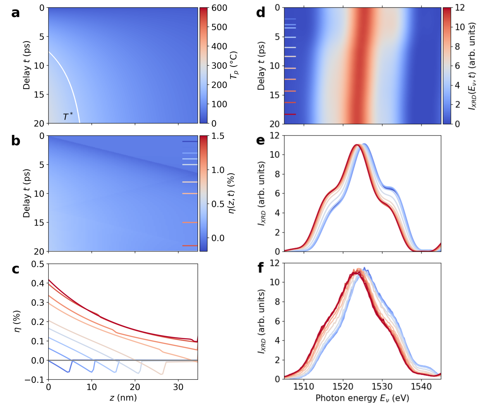
We observe an initial reduction of the tetragonal distortion, which goes hand in hand with lattice compression, then followed by lattice expansion. In particular, Figure 1b shows the (001) diffraction intensity of BTO as a function of the photon energy and at different pump-probe delays from to . At we observe the following changes to the Bragg peak as compared to the ground state (at ): a decrease in the diffraction intensity near the peak center, and a shift to higher photon energy, which implies a decrease in the out-of-plane lattice parameter , i.e., lattice compression (see gray curve in Figure 1b). To further explore this initial structural dynamics, we measure the delay dependence of , which quantifies the relative change of at the photon energy of the BTO peak with respect to the equilibrium value at negative delays. We observe a maximum diffraction intensity drop of at , with up to recovery to the equilibrium value at (Figure 1c and Figure S5). We assign the initial drop and recovery in diffraction intensity to the displacements of atoms within the BTO unit cell (inset of Figure 1c). Specifically, simulations based on the dynamical theory of diffraction (Figure S6) exclude the Debye-Waller effect and show that a decrease in the displacement between the Ti atom and the center of the O octahedron by can model the measured maximum change in peak diffraction intensity.
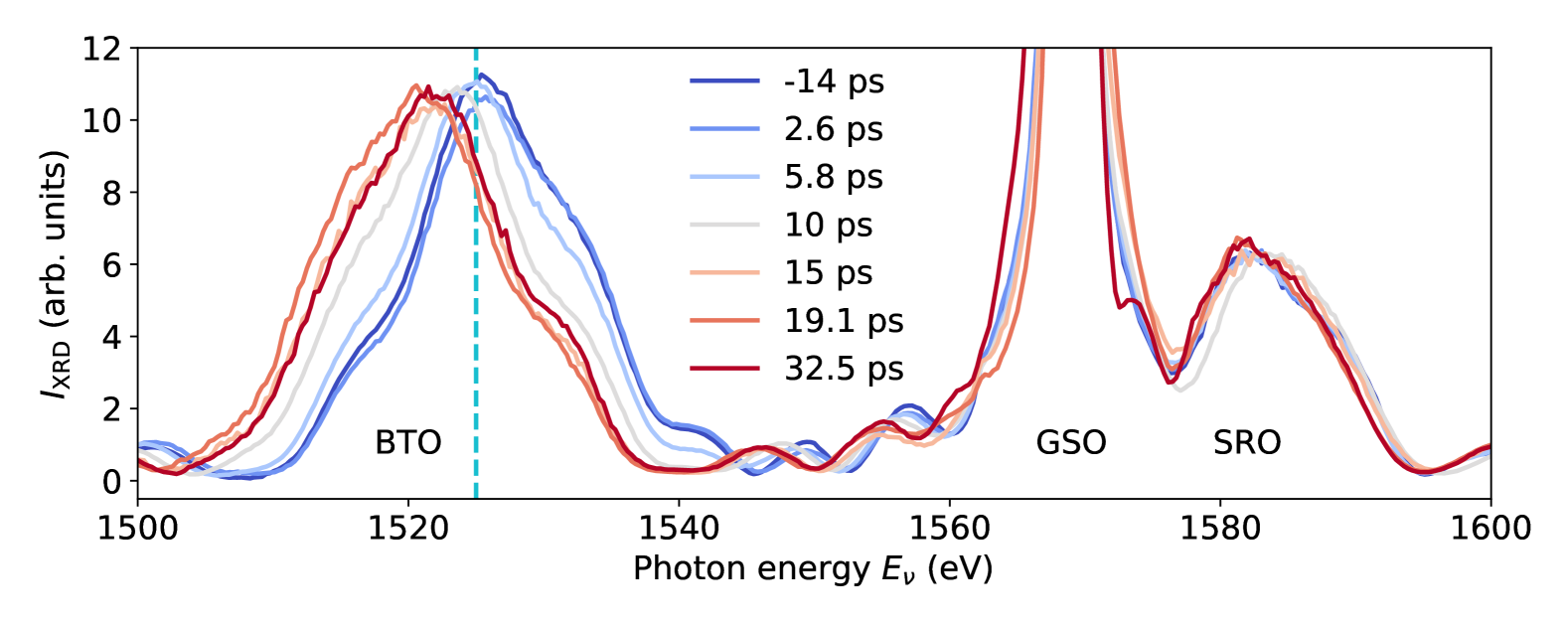
We focus next on the BTO (001) Bragg peak measured at longer time delays (Figure 1b). We observe that at are shifted toward lower photon energies, i.e., larger out-of-plane lattice parameters , with respect to at smaller delays . This can be clearly seen from the plot of the BTO out-of-plane strain , averaged over (Figure 1d). Here, , with and representing the average at a given and , respectively (see Methods). In Figure 1d, we find that: (i) the maximum compression of occurs at , (ii) increases linearly at a rate of in the range , and (iii) settles at at .
The model fitting data in Figure 1d is presented in the following. When a photon with energy is absorbed in BTO, electrons are photoexcited from the O 2p-derived valence band to the Ti 3d-derived conduction band [29, 30, 31]. The thermalization of photoexcited electrons leads to an increase in the electron temperature (), and to changes in the electronic system that can be modeled by the variation of the bandgap as a function of the electronic pressure () [4]. In turn, a modified electron system affects the interatomic potential, resulting in atomic motions and contributing to the deformation potential stress . Subsequently, photoexcited electrons transfer part of their excess energy () to the phonon system via electron-phonon scattering, increasing the phonon temperature () on the picosecond timescale. This, in turn, induces a lattice expansion dependent on the BTO linear expansion coefficient (), and contributes to the thermoelastic stress . The total stress[4, 32] generates a strain wave that propagates through the material of mass density at the longitudinal speed of sound . We solve analytically the two-temperature model (Supplementary Note 7) and the lattice strain wave equation (Supplementary Note 8) to obtain . Finally, we calculate the strain , averaged over , to fit the experimental data in Figure 1d. The main outcome of our fit model is a negative of the order of , in agreement with first-principles calculations[33], with a resulting bandgap decrease of about (Supplementary Note 10). The negative causes lattice compression within the first , when dominates over (inset of Figure 1d). Conversely, at larger time delays (), increases (Figure S17b) and the thermoelastic term becomes the dominant one, leading to lattice expansion (Figure S23).
Photoinduced ferroelectric polarization and electron dynamics
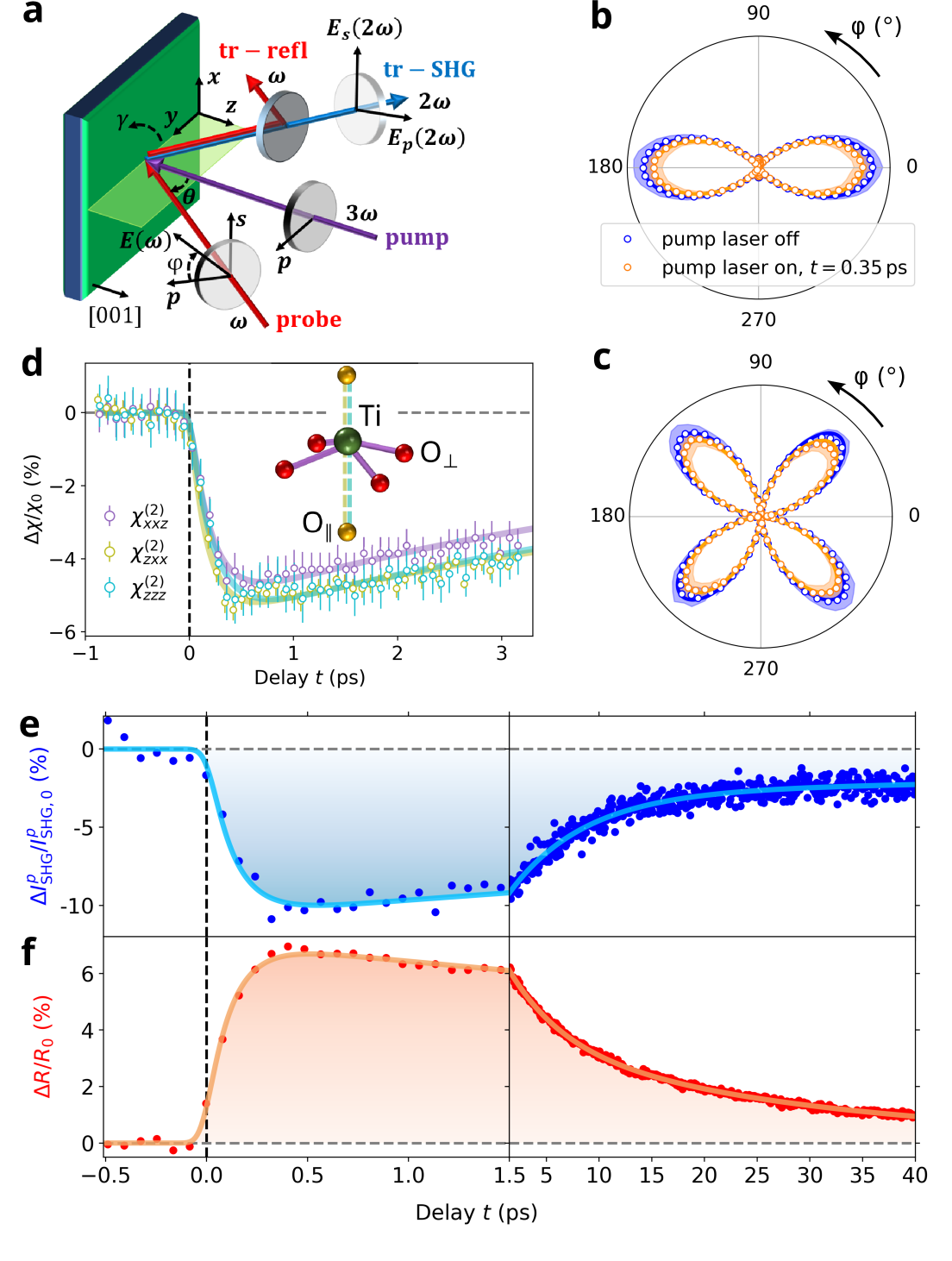
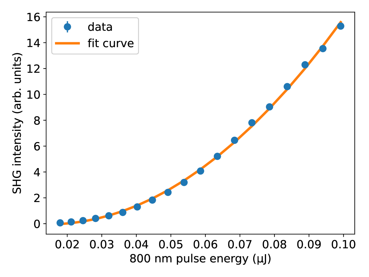
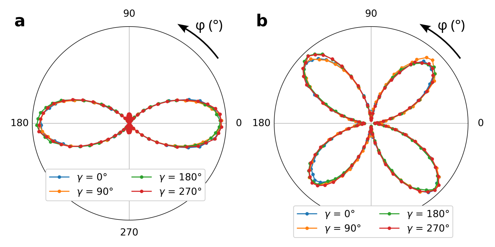
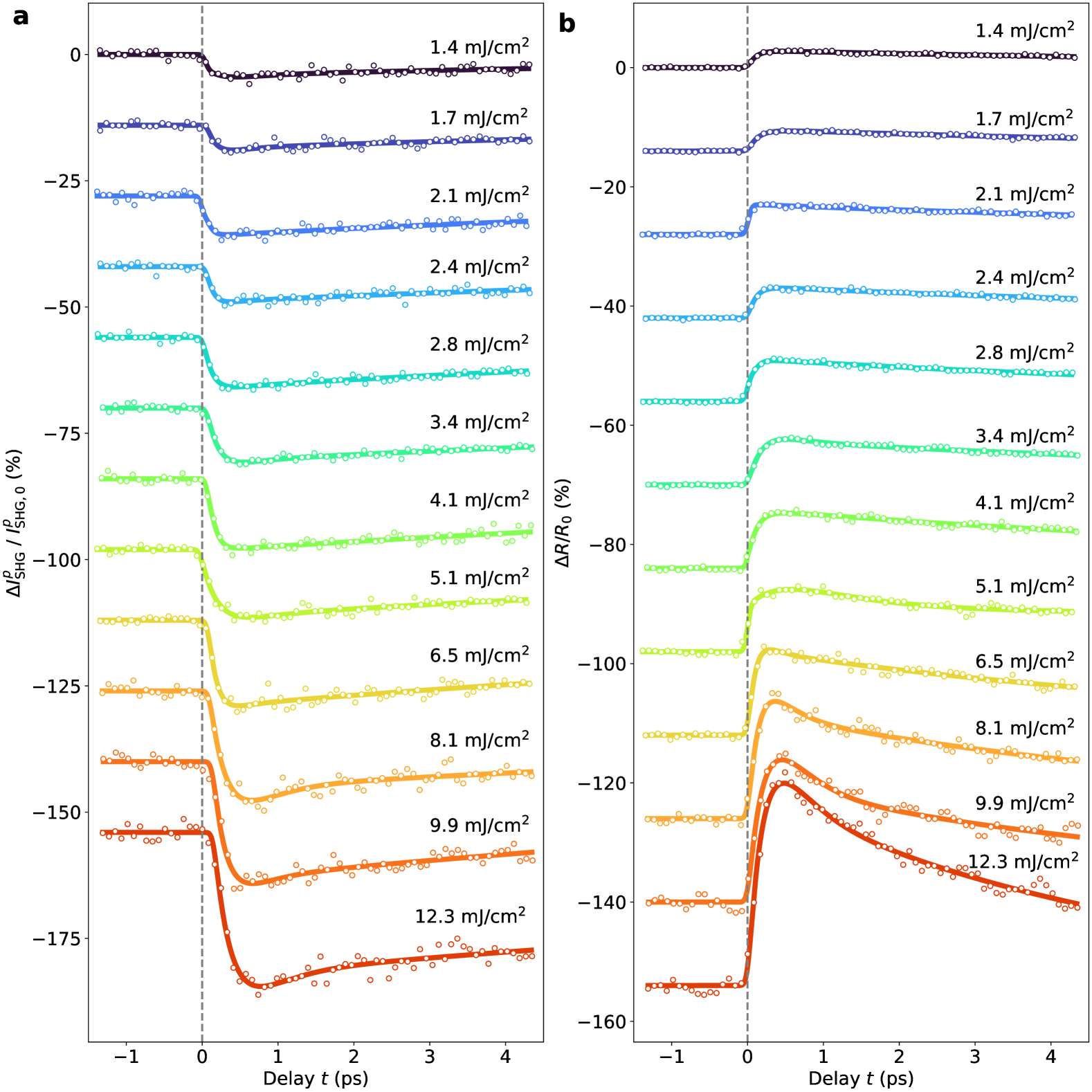
We turn now to investigating the dynamics of the ferroelectric polarization and of the photoexcited carriers [34, 35, 36, 37, 38], upon excitation of the BTO film by the same pump laser with fluence . Therefore, we perform tr-SHG experiments [39, 27] and simultaneously tr-refl in reflection geometry (Figure 2a). From SHG polarimetry, i.e., the dependence of SHG intensity on the polarization angle of the probe beam , we learn about the optical tensor elements of a material, and thus its symmetry[39]. By selecting either horizontal () or vertical () polarization of the SHG beam, we measure and , shown in Figures 2b and c (blue points) together with the respective fit curves (see Methods), which are based on the 4mm point group symmetry with the following nonzero tensor elements: , , and .
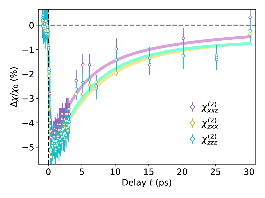
We observe a reduction of the BTO tetragonality, upon laser excitation, from the time evolution of , , and in the delay range . While the 4mm symmetry is preserved also after the pump excitation (orange points in Figures 2b-c), a laser-induced change in tetragonality is observed. To visualize it, we display the relative change of , , and as a function of delay (Figure 2d for and Figure S13 for ). The three tensor elements show similar dynamics, characterized by a fast fall time with the maximum drop after and two exponential recovery time constants of and . Interestingly, the tensor elements representative of the electric dipole along the out-of-plane direction ( and ) show a nearly identical time dependence and a larger relative change than , which refers to the in-plane electric dipole along the direction . The difference between (or ) and reaches after and decreases in a few tens of picoseconds (Figure S13). A purely thermal effect [40] would cause a uniform change of all tensor elements , whereas the measured different dynamics of indicates a time-dependent lattice distortion of non-thermal origin. In fact, TD-DFT calculations[29, 30] show that upon charge transfer, the Ti- bonds between Ti and apical atoms (parallel to ) are weakened more than Ti- bonds between Ti and basal atoms (perpendicular to ), with a resulting reduction of the tetragonal distortion (inset of Figure 2d). Consequently, it is intuitive to expect a larger amplitude of the induced electric dipole along the Ti- direction () with respect to the Ti- direction (in the plane), as experimentally demonstrated by our data.
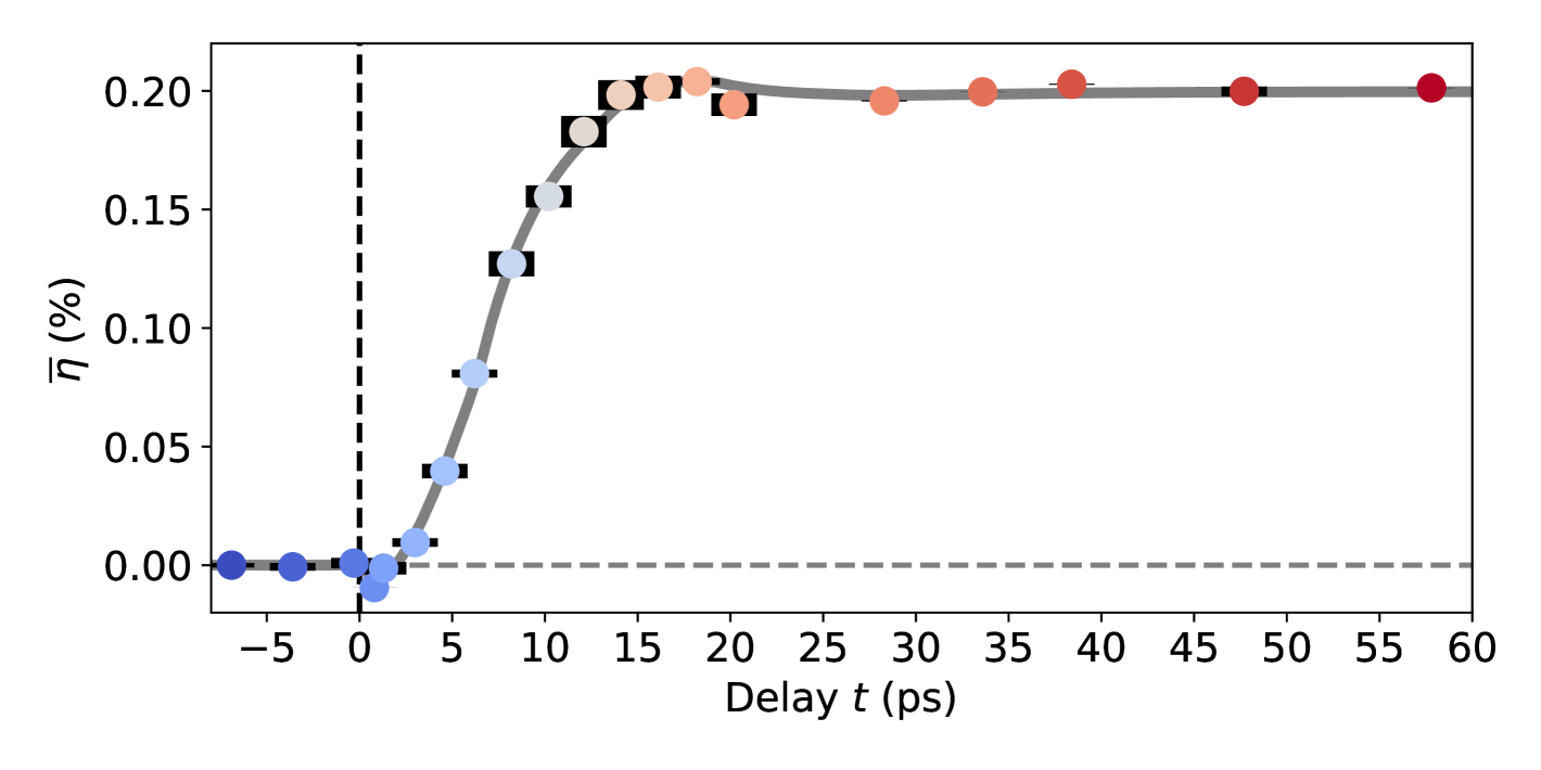
The proportionality gives direct access to the magnitude of the spontaneous polarization [39]. To this end, we measure the relative change as a function of pump-probe delay (Figure 2e), with the polarization of the probe beam fixed to the maximum of at (Figure 2b). Simultaneously, we measure the relative change in reflectivity as a function of pump-probe delay (Figure 2f). The data in Figure 2e [f] are well reproduced by a fit function consisting of the sum of three exponential decay terms, with fall [rise] time , and recovery times and , convoluted with a Gaussian function representing the experimental temporal resolution (Supplementary Note 2). The initial drop in SHG intensity by within is followed by and recovery times, resulting in a drop at (Figure 2e). At the same time, we observe a fast increase in reflectivity by within , followed by two recovery times, and (Figure 2f).
In both tr-SHG and tr-refl data, the time needed to reach the maximum relative change () might be due to the thermalization of photoexcited electrons via electron-electron scattering. Subsequently, thermalized electrons, which are higher in the conduction band, move to the bottom of the conduction band, transferring energy to the phonon system, and recombining with holes in the valence band via electron-phonon scattering[41, 4, 37] or radiatively[42]. These processes are characterized by the recovery times and . Both and recovery constants of are larger than those of because the dynamics of the spontaneous polarization results from the convolution of the faster dynamics of photoexcited carriers (seen by tr-refl) and the slower dynamics of atoms.
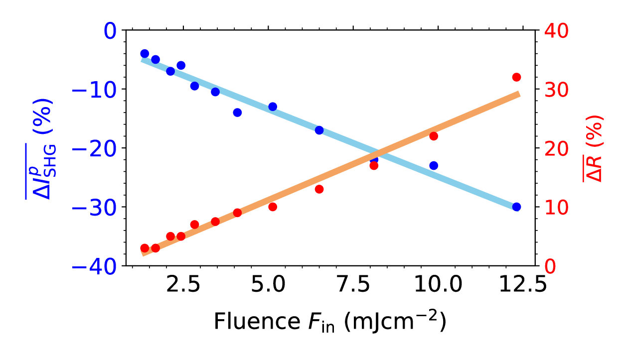
To interpret the SHG intensity drop and the reflectivity increase, it is useful to express the spontaneous polarization as[22, 43]: , where is the volume of the unit cell, is the Born effective charge and is the out-of-plane displacement of atom . The above-bandgap photoexcitation transfers electrons from the O 2p-derived valence band to the Ti 3d-derived conduction band of BTO. This charge transfer from O to Ti atoms reduces the corresponding charges . We attribute changes in to changes in photoexcited carrier density [35, 36, 37], thus contributing to , while results from changes in both and . After , before atomic movements can occur, the increase in carrier density is responsible for the measured decrease in and increase in , shown in Figures 2e-f. This interpretation is corroborated by the increase of the maximum relative change of both and with pump fluence (Figure S14 and Figure S15).
Discussion
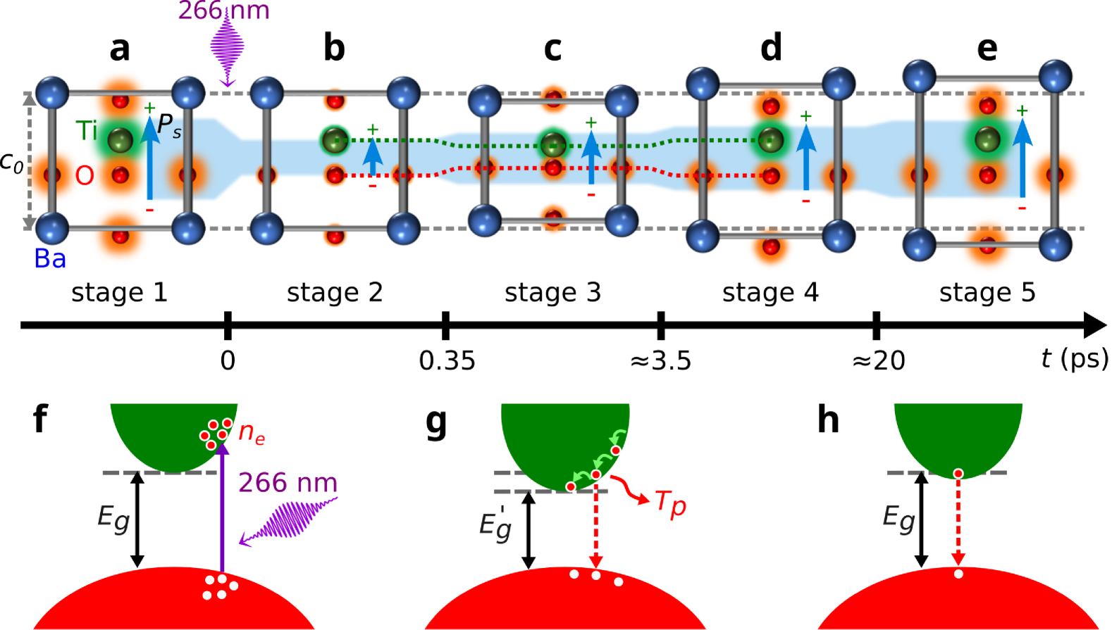
We present here a unified picture in five stages of the lattice, polarization, and electron dynamics data presented above. Our observations are summarized in Figures 3a-e, and the physical mechanisms involved are sketched in Figures 3f-h. Before the arrival of the pump laser, the BTO is characterized by an out-of-plane polarization with given Born effective charges at each atomic site (stage 1, Figure 3a). Upon absorption of the pump laser at , electrons move from the occupied O-derived valence band to the unoccupied Ti-derived conduction band (Figure 3f). Within we observe the maximum increase in the photoexcited carrier density , as indicated by the increase in . This charge transfer reduces the Born effective charges at Ti and O atoms, thereby decreasing the spontaneous polarization , as indicated by the decrease in (stage 2, Figure 3b). A smaller is also consistent with a larger screening of long-range Coulomb interactions, which favor off-center atomic displacements and thus are responsible for the polar order. This effect is modeled by DFT calculations[44, 45], showing that an increase in photoexcited carriers in the conduction band of BTO indeed tends to induce a phase transition from the ferroelectric to the paraelectric phase. Moreover, TD-DFT calculations[29, 30] predict that such photoinduced change of BTO electronic structure weakens more significantly Ti-O∥ bonds, parallel to , as compared to Ti-O⟂ bonds, perpendicular to . We demonstrate this effect experimentally by measuring a larger change of the out-of-plane tensor elements (, ) as compared to the in-plane tensor element (). In stage 2, in contrast to the maximum change in carrier density and polarization , the lattice remains unperturbed: this marks the onset of the decoupling between polarization and strain. At these early time delays, the bulk photovoltaic effect (BPVE) [12] and the Schottky interface effect [11] could potentially play a role, but we explain in the following why they are not dominant in our experiments.
First, in photoexcited ferroelectric materials it is common to observe the BPVE, i.e., the generation of photovoltage under light illumination [46, 47, 48]. The BPVE occurs under two conditions: the presence of a noncentrosymmetrical crystal and the excitation of nonthermalized electrons [46]. In our system both conditions are satisfied shortly after , i.e., before hot electron thermalization takes place (Figure 3f). In BTO, if the light polarization is perpendicular to the spontaneous polarization , the induced photovoltage is parallel to [49, 50]. This enhances and induces, via the inverse piezoelectric effect, lattice expansion, similarly to what was observed in BiFeO3 [51]. However, in our study, although the polarization of the pump laser is perpendicular to (Figure 2a), within , when electrons are non-thermal and BFVE could potentially play a role, we see a decrease in (Figure 2e). Hence, we conclude that BPVE is not a dominant effect in our experiments. In fact, this observation can be explained by the wavelength dependence of the BPVE, which shows a maximum when the photon energy is close to , as observed, e.g., in Refs. [12, 52]. In contrast, in BTO at the contribution of BVPE is negligible, as observed in experiments [49, 50] and calculations [47].
Second, ferroelectric thin films grown on a metal substrate form a Schottky interface, where the electron-hole pairs generated by light absorption are separated by the built-in voltage of the Schottky barrier and cause a power-independent enhancement of the polarization for pointing up (toward the surface) [11]. This effect can be excluded as responsible for our experimental observations because: (i) although our sample has pointing up (Figure S3), we see a decrease in , and (ii) the measured change in linearly depends on the incident fluence (Figure S14). In fact, the Schottky interface effect is expected to play a significant role for films of thickness or thinner [11], and to be negligible in our case due to the three-fold greater film thickness.
In the delay range (stage 3, Figure 3c), we observe polarization and strain following opposite trends. In fact, while the displacement between Ti and the center of the O octahedron as well as the strain decreases, starts to increase. This is attributed to the initial recombination of photoexcited carriers, suggested by the incipient recovery in . At this stage, we also observe lattice compression caused by the negative parameter via the deformation potential. Our observation is in line with theory [53, 45, 30] predicting a reduced bandgap due to the presence of photoinduced carrier density (Figure 3g). Moreover, lattice contraction via the inverse piezoelectric effect is also consistent with an overall reduced caused by photoexcited carriers [54].
In the delay range (stage 4, Figure 3d), the relative displacement between Ti and O atoms tends to restore the ground state with a larger . At the same time, the relaxation of photocarriers to the top of the conduction band and their recombination result in a further increase of the Born effective charges, and an energy transfer to the phonon temperature (Figure 3g), which, in turn, leads to lattice expansion. The latter effects persist up to .
At (stage 5, Figure 3e), together with a further relaxation of the electronic system toward equilibrium, we observe a saturation of the BTO average strain. This results in a metastable state with a slightly reduced and a significantly increased out-of-plane strain with respect to the ground state. The reduced is attributed to the presence of residual photoexcited carriers in the conduction band (Figure 3h), while the increased out-of-plane strain is due to the thermoelastic contribution. We exclude the depolarization field screening as the main driving effect for the transient tensile strain seen in our experiments, because it would lead to the typical saturation of the strain with increasing pump fluence [55]. For example, in PbTiO3 [12] the metastable lattice strain reaches saturation with laser fluences of . Conversely, in our study, we employ two orders of magnitude larger pump fluence and still the metastable strain scales approximately linearly with the pump fluence (Figure 1d and Figure S18). In addition, on the timescale, the deformation potential plays a minor role (Figure S23), thus its influence on the bandgap is expected to be marginal. Interestingly, although the out-of-plane lattice parameter is larger than in the ground state (), the polarization is still smaller compared to equilibrium. This underscores the persistence of the decoupling between polarization and strain. Quantitatively, we estimate that in stage 5 the contribution of photoexcited electrons to has larger magnitude than the structural contribution from the strain (Supplementary Note 11).
In summary, we demonstrate that, with an above-bandgap laser excitation, an ultrafast decoupling of spontaneous polarization and strain can be achieved and measured. We assign this effect to the dominant contribution of photoexcited electrons in determining the spontaneous polarization when the system is out of equilibrium, and show that for an accurate description and fundamental understanding of a ferroelectric material in a photoexcited state, it is essential to combine multiple techniques that address the dynamical evolution of the various degrees of freedom, i.e., lattice, ferroelectric polarization, and electrons. The decoupling of polarization from the strain offers the opportunity to change paradigm from strain engineering [56] to light-induced polarization engineering, thereby lifting the constraint of selecting among a limited number of substrates [24] or designing freestanding membranes [26] to tune the spontaneous polarization. Moreover, by softening the Ti-O∥ bonds, we bring BTO to an excited state, where it could be further modified by light to achieve stable and reversible polarization switching at lower fluences than otherwise needed when starting from the ground state [21]. Finally, the transient and reversible control of the spontaneous polarization, shown in this study, offers a pathway to control by light both electric and magnetic degrees of freedom in multiferroic materials.
Methods
Sample preparation and characterization
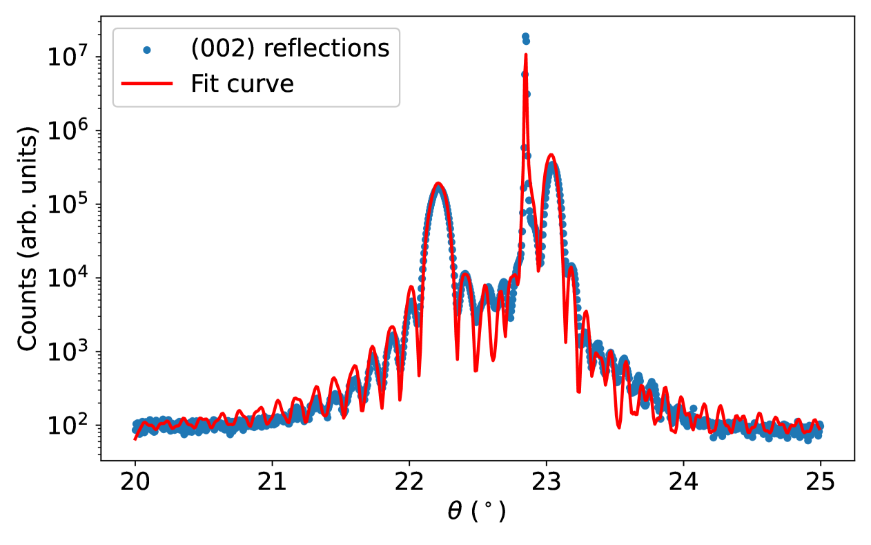
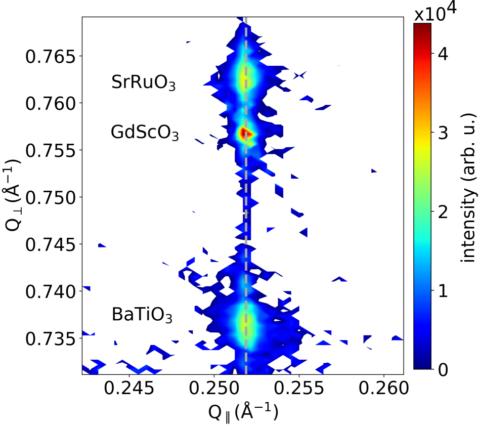
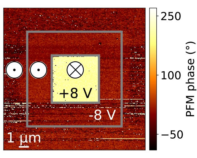
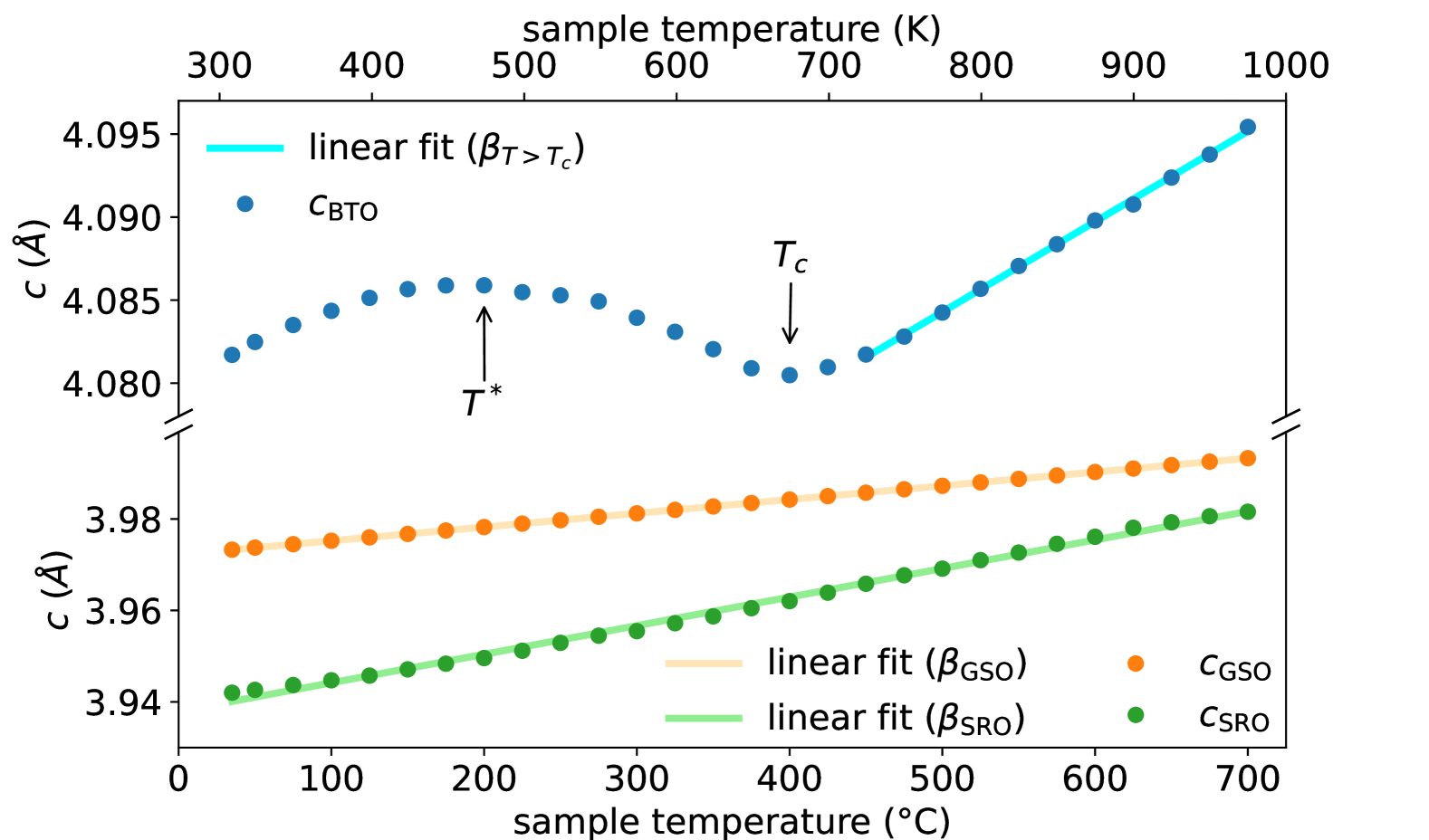
The epitaxial bilayers BTO/SRO were grown on a GSO substrate using pulsed laser deposition. The ceramic targets of SRO and BTO were away from the substrate and ablated using a KrF excimer laser (, fluence , repetition rate). The deposition of SRO and BTO layers was conducted in O2 atmosphere with pressure pO2 = 100 mTorr and deposition temperatures of and , respectively. Sample cooling with the rate of was conducted in the environment of saturated O2 (pO2 = mTorr) to prevent the formation of oxygen vacancies. The thicknesses of BTO and SRO layers, and are extracted from a - scan of the as-grown sample around the (002) reflections (Figure S1), while the GSO substrate is thick. We determine the out-of-plane lattice parameters , , and by means of the reciprocal space map shown in Figure S2. The in-plane lattice parameter , common to BTO, SRO and GSO, indicates that both BTO and SRO thin films are coherently strained to the substrate. Furthermore, the absence of satellite peaks in Figure S2 suggests the existence of a BTO monodomain. We determine that the spontaneous polarization of the as-grown sample points upward (toward the surface) by means of piezoresponse force microscopy (Figure S3). The linear expansion coefficients of BTO above , of SRO and GSO in the temperature range are determined by - scans as a function of sample temperature (Figure S4).
Time-resolved X-ray diffraction
Time-resolved X-ray diffraction experiments were performed at the Spectroscopy and Coherent Scattering instrument (SCS) of the European X-Ray Free-Electron Laser Facility (EuXFEL), using an optical laser (OL) as pump and the XFEL as probe. The XFEL pulse pattern consisted of pulse trains at a repetition rate of , with pulses per train at the intratrain repetition rate of . The full width at half maximum (FWHM) of the XFEL spectrum was . To reduce the energy bandwidth, the XFEL beam was monochromatized using a variable line spacing grating with lines/mm in the first diffraction order and exit slits with a gap of , providing an energy resolution of . The nominal pulse duration of the XFEL pulses was , with pulse stretching at the monochromator grating of (FWHM). The XFEL pulses, with initial energy of per pulse, were then attenuated by transmission through a gas attenuator (GATT), consisting of a volume containing gas at a variable pressure. In order to prevent detector saturation, the transmission of the GATT was set to have per pulse at the sample. The XFEL pulse energy was measured by an X-ray gas monitor detector (XGM), located upstream of the sample, just before the Kirkpatrick-Baez (KB) mirrors. The latter were used to focus the XFEL beam at the sample to a spot size of (determined by knife edge scans), where is defined as the distance from the beam axis where the intensity drops to of the value on the beam axis. The angle of incidence (defined from the sample surface) of XFEL and OL beams at the sample was and , respectively. The intensity of each XFEL pulse diffracted by the sample was measured by a Si avalanche photodiode (APD, model SAR3000G1X, Laser Components), converted to a voltage pulse and digitized. To prevent the pump laser intensity from reaching the APD, the latter was equipped with a filter made of Ti, deposited on polyimide.
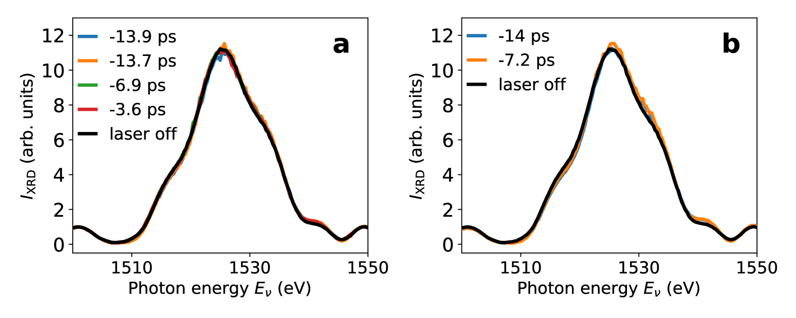
The pump laser had a central wavelength of , the same pulse pattern as the XFEL with pulse duration of , and beam size , determined by knife edge scans. The transmittance profile of the laser in our BTO/SRO/GSO sample is reported in Supplementary Note 6.1. The incident pump laser fluence at the sample was , and we verified that diffraction curves measured at negative delays coincide with those measured without the pump laser (Figure S7). This confirms the reversibility of the pump effect induced by UV laser light. The temporal overlap between XFEL and OL was determined as detailed in Figure S8. The diffracted intensity of the XFEL pulses in a train was averaged and the corresponding time delay of the OL was corrected by the respective bunch arrival monitor (BAM) value, obtaining a time resolution (Supplementary Note 4). Data measured with incident pump laser fluence of are reported in Supplementary Note 8 and Supplementary Note 9.
In general, two kinds of tr-XRD experiments were performed: photon energy scans at a fixed pump-probe delays (Figure 1b and Figure S5), and time delay scans at a fixed photon energy (Figure 1c and Figure S8). The energy scans were carried out by a simultaneous movement of the monochromator grating and the undulators gap, such to have always the peak of the XFEL spectrum at the desired photon energy. From the energy scans at different , the out-of-plane lattice parameters and are calculated as the center-of-mass of the BTO diffraction intensity and refer to the average over (). Specifically, the BTO average out-of-plane parameters is calculated from the corresponding (001) Bragg peaks using the Bragg condition , where is the average of energy values, around the (001) BTO peak, weighted by . Energy scans at different pump-probe delays over the photon energy range covering also GSO (001) and SRO (001) Bragg peaks are reported in Figure S9.
Time-resolved SHG and reflectivity
Time-resolved Second Harmonic Generation and time-resolved reflectivity experiments were performed at the SCS instrument of the EuXFEL using the same optical laser employed for tr-XRD experiments and the same pulse pattern. A sketch of the setup is shown in Figure 2a. The probe beam at frequency (red arrow) impinges on the sample at angle (defined from the normal to the surface) with polarization defined by the angle and varied by rotating a half waveplate. The angle [] refers to [] polarized light. The pump beam at frequency (purple arrow) impinges on the sample at normal incidence with polarization. The probe beam is then reflected by the sample and a dichroic mirror before reaching a Si photodiode. The latter is used to measure tr-refl of our sample. The beam at frequency (blue arrow) is the SHG signal generated in the BTO sample (Figure S11). This SHG beam is transmitted through the dichroic mirror and Glan polarizer, which is set to select either the or component of the electric field, corresponding to the -out or -out configuration, respectively. Finally, the SHG beam is filtered by a bandpass filter before reaching a photomultiplier (model H10721-210-Y004, Hamamatsu). The azimuthal rotation of the sample around the axis is defined by the angle . The independence of both polar plots of and from confirms the out-of-plane nature of the spontaneous polarization of our BTO sample (Figure S12). Both Si photodiode and photomultiplier measure respectively the reflectivity and SHG signal of each OL pulse in the train. The pulse duration of the probe and pump beams were approximately and , providing a time resolution of . The beam sizes of and beams, determined by knife edge scans, were and , respectively. The penetration depths of , and laser beams in BTO are reported in Supplementary Note 6.2. While the fluence of the probe beam was kept at , the fluence of the pump beam was set to for the data displayed in Figure 2. tr-SHG and tr-refl data with fluences between and are reported in Figure S14 and Figure S15.
In general, given the incoming electric field with components and at frequency along and directions, the electric dipole polarization induced in the material at frequency along the direction is , where is the second-order susceptibility, i.e., a third rank tensor reflecting the symmetry of the material. Each direction , , can be , or , or directions (Figure 2a). By selecting or polarization of the SHG beam, we measure or , which, for a BTO single crystal with 4mm point group symmetry, can be expressed as[39, 11]:
| (1) |
| (2) |
The resulting ratios of the tensor elements in Figure 2b-c, and , reflect a thin film under tensile out-of-plane stress[57]. The good quality of the fit curves in Figure 2b-c confirms that our BTO thin film has 4mm point group symmetry. The minor discrepancies between data and fit model might be due to the fact that our BTO thin film is coherently strained to the substrate, and this leads to the appearance of additional minor nonzero tensor elements [58].
Data availability
Data recorded for the experiment at the European XFEL are available at doi:10.22003/XFEL.EU-DATA-003481-00. Source data are provided with this paper. Further experimental data as well as the simulation data that support the findings of this study are available from the corresponding author upon reasonable request.
Code availability
Codes generated during the current study are available from the corresponding author on reasonable request.
Acknowledgements
We acknowledge the European XFEL in Schenefeld, Germany, for provision of the XFEL beamtime at the SCS scientific instrument and would like to thank the staff for their assistance. D.P. acknowledges funding from ’la Caixa’ Foundation fellowship (ID 100010434) and the Spanish Ministry of Industry, Economy and Competitiveness (MINECO), grant no PID2019-109931GB-I00. The ICN2 is funded by the CERCA programme/Generalitat de Catalunya and by the Severo Ochoa Centres of Excellence Programme, funded by the Spanish Research Agency (AEI, CEX2021-001214-S). T.C.A. acknowledges funding from the Heisenberg Resonant Inelastic X-ray Scattering (hRIXS) Consortium. We thank D. Hickin for support with the automation of tr-SHG measurements. We thank A. Reich and J.T. Delitz for the design of mechanical components used in tr-XRD experiments. We are grateful to M. Altarelli for careful reading of the manuscript.
Author contributions
G.Merc., with input from L.P.H., G.C., I.A.V., J.Z. and T.L.L., conceived the experiments. G.C. and I.S., with input from G.Merc., designed the sample. J.M.C.R manufactured the sample and D.P. characterized it with - scan, RSM and PFM. L.P.H, D.P., G.N.H., R.C., L.M., M.T., S.G., T.C.A., G.Merz., S.P., J.Sc., Z.Y., I.A.V. and G.Merc. performed tr-XRD experiments. C.C. developed an online analysis tool to visualize tr-XRD data in real time. G.Merc. and L.P.H. performed tr-SHG and tr-refl experiments. J.Sa. performed - measurements at different sample temperatures. L.P.H. and G.Merc. analyzed all the data. L.P.H. modeled tr-XRD and tr-SHG data. G.Merc., A.S., K.R. and I.A.V. supervised the project. G.Merc. wrote the manuscript, drafted by L.P.H., and with input from all authors. All authors provided critical feedback and helped shape the research, analysis and manuscript.
Ethics declarations
The authors declare no competing interests.
Supplementary Information for:
Ultrafast decoupling of polarization and strain in ferroelectric
Supplementary Note 1 Sample characterization
Supplementary Note 2 Fit function of tr-XRD, tr-SHG and tr-refl delay scans
The function used to fit the delay scans presented in this work is:
| (S1) |
Equation (S1) is the convolution of the sum of three exponential decays , with the Gaussian function , where and is the time resolution (FWHM) of our experiment (Supplementary Note 4). The resulting fit function can be written as:
| (S2) |
with the time constants , , , and and the amplitudes , , and as fit parameters.
Supplementary Note 3 XRD data
Supplementary Note 4 Bunch arrival time monitor and time resolution of tr-XRD experiments
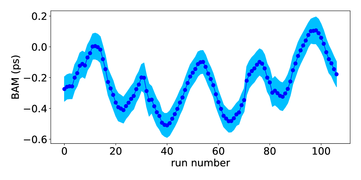
The bunch arrival time monitor (BAM) at the European XFEL tracks the arrival time of electron bunches in each pulse train, providing invaluable information to improve the time resolution of pump-probe experiments [62, 63]. The BAM measures the electron bunch arrival time with respect to the master clock that is also used to synchronize the pump laser. We employ the most downstream BAM, located at the end of the accelerator tunnel ( from the laser gun) and about upstream of the interaction point at the sample position. In previous time-resolved experiments at the SCS Instrument, it has been observed that the time drifts measured by the BAM are amplified by at the interaction point [64]. In practice, this translates in a further correction of up to few tens of femtoseconds. In our experiments, the exact amplification coefficient is not known, thus we assume a direct proportionality between BAM and at the experiment, where indicates the temporal overlap between XFEL and optical laser. This assumption is justified by the dynamics of tr-XRD experiments taking place on the picosecond timescale (Figure 1).
We measure a standard deviation of the BAM within a pulse train of , and a standard deviation of the BAM from train to train of . Most importantly, slow drifts of the arrival time of FEL pulses over the course of hours are present and shown in Figure S10 for each recorded run. This indicates that without BAM correction, the time resolution of our experiments might be limited up to , if we average non-consecutive runs. To improve our time resolution, the time delays of our data, indicating the relative time between FEL and optical laser pulses, are corrected for each pulse train according to the average BAM value of the respective pulse train. Thus, the resulting expected time resolution is . This assumes an FEL pulse duration of , including the nominal pulse duration [65] and the pulse stretching at the monochromator of (FWHM) [66], a pulse-to-pulse jitter in the train of , an optical laser pulse duration of and temporal jitter of .
Supplementary Note 5 SHG and reflectivity data
Supplementary Note 6 Sample properties
Supplementary Note 6.1 Transmittance profile of beam in BTO/SRO/GSO
The transmittance of the beam in our BTO/SRO/GSO sample, displayed in Figure S16, is calculated as:
| (S3) |
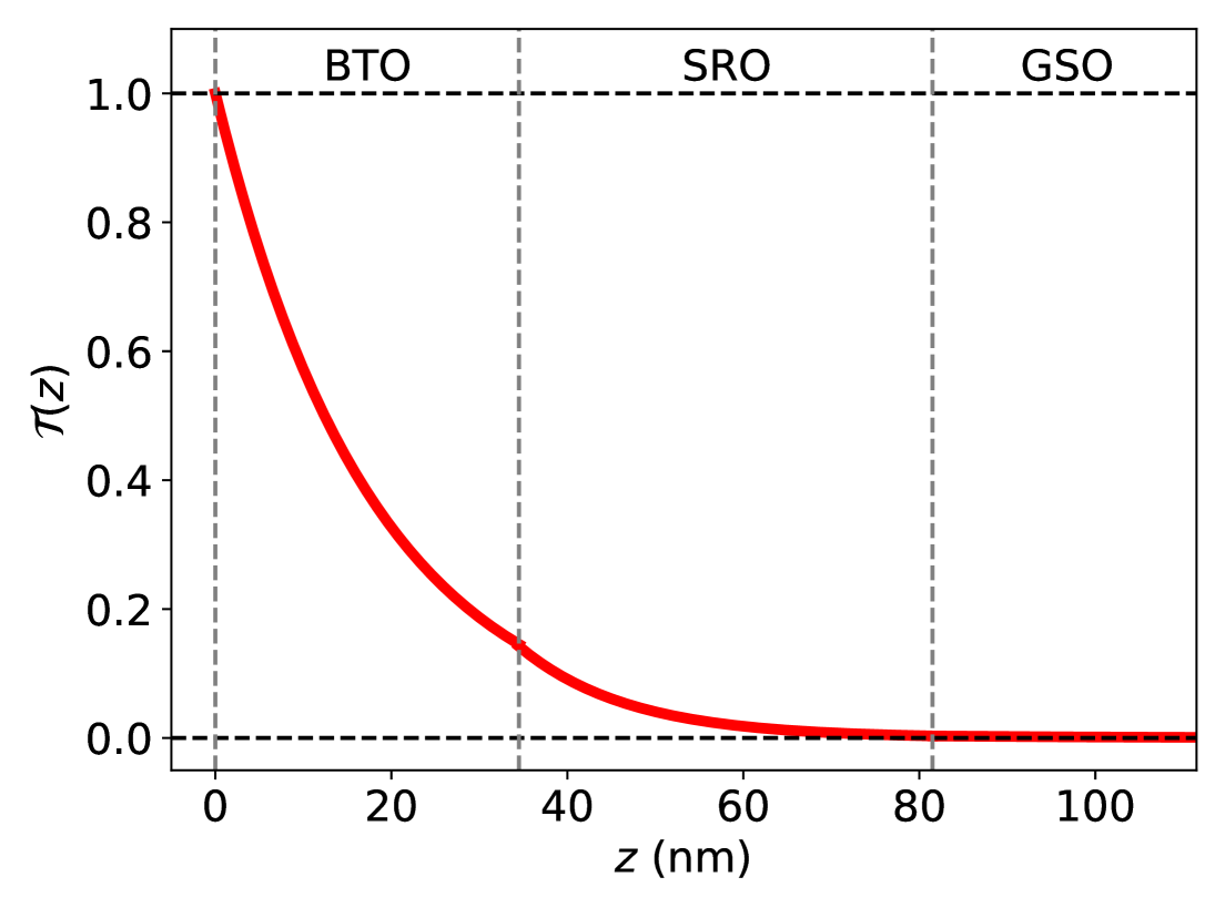
The penetration depths , and are calculated as detailed in Supplementary Note 6.2. The reflections at the air-BTO, BTO-SRO, and SRO-GSO interfaces (Table S2) are determined by using Snell’s law and the Fresnel equation for -polarized light . Here, and are the real part of at the two sides of the interface, while and are the angles of the incident and the transmitted beam with respect to the surface normal, with . The index of refraction of SRO and GSO are calculated from Ref. [68], as detailed in Supplementary Note 6.2, while the index of refraction of the BTO thin film is determined from ellipsometry data at in Ref. [28].
Given the parameters above (summarized in Table S2), the absorbed fluences in the BTO and SRO thin films are calculated as:
| (S4) |
| (S5) |
and are reported in Table S1.
| () | () | () |
|---|---|---|
| 1.4 | ||
| 2.7 |
Supplementary Note 6.2 Penetration depths
The absorption coefficient of the pump laser in our BTO thin film is determined based on the study of as a function of strain in Ref. [28]. For a compressive strain of , the penetration depth is . The penetration depths in the SRO thin film and in the GSO substrate are determined from the respective dielectric constants and , reported in Ref. [68]. Specifically, , where is the wavelength of the pump laser, and is the imaginary part of the complex index of refraction , with , , and . The penetration depth of and in BTO, and , are obtained from the equations above, calculating the complex dielectric function as , where , with and reported in Ref. [28]. Due to the large penetration depths and , we probe the entire BTO thickness ().
| constants | unit | BTO | SRO | GSO |
|---|---|---|---|---|
| - | ||||
| [69] | [70] | |||
| [69] | [70] | |||
| [71] | ||||
| [72] | ||||
| () | ||||
| [73] | [69] | [70] | ||
| [73] | [69] | [70] | ||
| [71] | ||||
| [71] | - | 0.3 | ||
| [41] | ||||
| - |
Supplementary Note 7 Two-temperature model
Electron and phonon temperatures, and , result from the analytical solution of the two-temperature model (2TM), consisting of the following coupled equations [74]:
| (S6) | ||||
where and are volumetric heat capacities, respectively, and is the electron-phonon coupling. The source term represents the absorbed power density () of the pump laser in our sample as a function of and . It is defined as , where is the pump absorbed fluence (Supplementary Note 6.1), is the penetration depth (Supplementary Note 6.2), is the angle of the transmitted optical beam with respect to the surface normal, and is the optical laser pulse duration (Supplementary Note 4).
In general, equation (S6) contains also the diffusion terms and , where and are carrier and thermal conductivity, respectively. In the particular case of BTO, carrier and thermal diffusion terms can be neglected because the parameters and are relatively small. Here, the electron diffusion coefficient is calculated from the Einstein relation , where is the BTO electron mobility [75], is the Boltzmann constant, is the sample temperature and is the electron charge, while the BTO thermal diffusivity [73] is .
We turn now to discuss the volumetric heat capacities and . Electron and phonon volumetric heat capacities of SRO and GSO are taken from Refs. [69, 70], assuming . This assumption is justified by the fact that in GSO the transmittance of the beam is essentially , while in the SRO thin film only of the incident fluence is absorbed. For the absorbed fluence (Supplementary Note 6.1), the maximum temperature increase [41] in SRO is , with a consequent increase of of only . Conversely, increases by , but the absolute value remains one order of magnitude smaller than . The volumetric heat capacity as a function of is reported in Ref. [76]. Given the weak temperature dependence for , we consider and calculate and , for and (Supplementary Note 6.1), respectively. Due to the weak dependence on , the average of between and yields the self-consistent result of [76]. Finally, to estimate , we rely on the available data from other titanates, e.g. SrTiO3 [77] and CaTiO3 [78], and observe that they have an average ratio for the ranges considered here. This yields . Although is a temperature-dependent quantity, for simplicity, we assume it to be constant here. For completeness, all the physical constants employed in the solution of the 2TM are reported in Table S2.
We focus now on the analytical solution of the 2TM. The second equation of equation (S6) can be written as:
| (S7) |
which is then inserted in the first equation of (S6) and yields the following second order differential equation of :
| (S8) |
Given the following initial and boundary conditions: , , , we can derive the lattice temperature as an analytical solution of equation (S8):
| (S9) |
where , , and . Substituting equation (S9) in equation (S7) we obtain the electron temperature :
| (S10) |
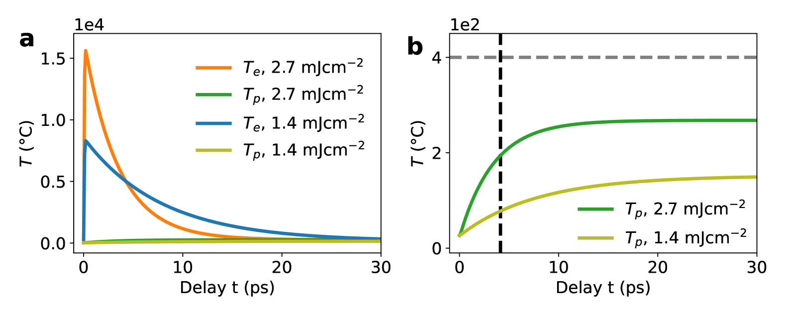
The dependence of and (averaged over ) on the delay is reported in Figure S17 for the two incident pump fluences and and the corresponding fit parameter (Table S3), while Figure S22a and Figure S21a report the 2D maps of as a function of delay and depth at the respective fluences.
Supplementary Note 8 Strain model
The total stress experienced by our sample upon optical laser excitation can be written as [32, 4]:
| (S11) |
where is the Young’s modulus, is the mass density and is the longitudinal speed of sound (Table S2). The first term in equation (S11) indicates the direct relationship between the stress , a force that induces a deformation of the material, and the strain that represents the resulting deformation of the material. The stress causes the generation of a strain wave that propagates through the material and across the interface to the layer below. In equation (S11), indicates the variation of the bandgap as a function of the electronic pressure, and is the linear expansion coefficient.
Equation (S11) can be written more explicitly as [32]:
| (S12) |
where is the carrier density [4] (with unit ), is the bulk modulus (Table S2), is the sample temperature at equilibrium, and is the total energy density transferred from the optical photons to the electronic subsystem [4]. We consider here only the dependence of , and on the direction (sample depth). This one-dimensional approximation is justified by the large ratio between the laser excited area and the BTO thickness, leading to the film contraction/expansion only along the surface normal on the few tens of picoseconds timescale.
The relation between the stress and the atomic displacement is described by the following one-dimensional lattice strain wave equation [41]:
| (S13) |
which can be recast as a function of :
| (S14) |
Substituting equation (S12) in equation (S14) yields:
| (S15) |
Given the initial conditions [41] , , , equation (S15) provides the out-of-plane strain profile by solving the following analytical integrals [79]:
| (S16) |
where . Electron and phonon temperatures, and , are determined using the 2TM (Supplementary Note 7).
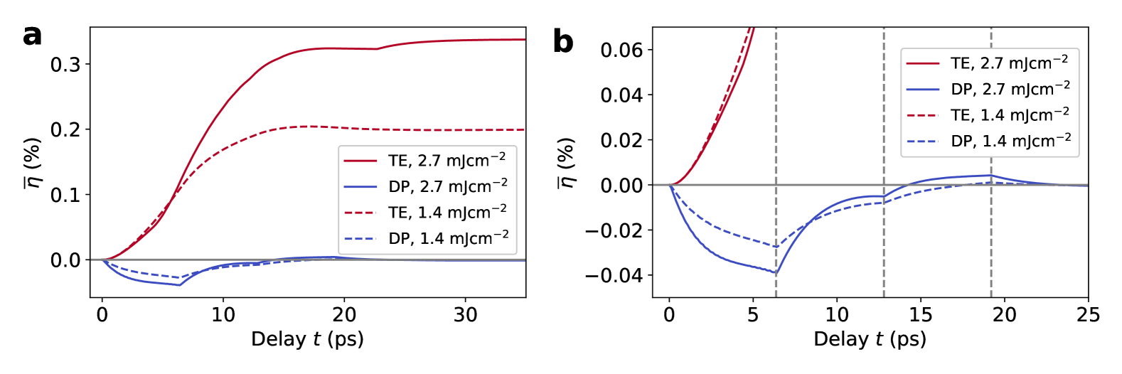
Since the optical pump laser is absorbed mostly in the BTO thin film, but partially also in the SRO layer, there will be two strain waves originating at the vacuum/BTO and the BTO/SRO interfaces. These strain waves propagate through the sample and reflect at each interface, with acoustic reflection coefficients (Table S2). The almost identical acoustic impedance of SRO and GSO, leads to a at the SRO/GSO interface. Conversely, the strain wave undergoes a reflection at the BTO/SRO interface and reflection at the interface with vacuum, given the acoustic impedance (Table S2). The superposition of the generated and reflected strain waves yields a total strain wave , which is then averaged over the BTO film thickness to obtain . This quantity is used to fit the experimental average strain data obtained from tr-XRD measurements for (Figure 1d) and for (Figure S18), with the resulting fit parameters (, , and ) reported in Table S3. The parameter has been discussed in the main text, we focus here on the discussion of , and fit results, while the calculations based on our strain model are presented in Supplementary Note 8.
| () | () | () | g () |
|---|---|---|---|
| 1.4 | |||
| 2.7 |
The linear expansion coefficient is the fit parameter referring to the average in the range , with Curie temperature . While for , the linear expansion coefficient is constant and positive (), it is positive for , and negative for (Figure S4). In our sample, the temperature below at which changes sign is (Figure S4). Based on our model, in the metastable state (), only of the BTO film is at for , while of the BTO film is at for (Figure S19). As a result, in the latter case the portion of the sample at is larger than in the former case, thus is expected to be smaller, as shown by our fit results (Table S3). At the same time, for both fluences, the larger portion of the sample () is at , hence is expected to be positive, as obtained by our fit results.
The electron-phonon coupling of the 2TM (Supplementary Note 7) is a temperature dependent quantity, however for simplicity in our model it is assumed to be constant, similarly to most current investigations of short-pulse laser excitation [80]. In general, the dependence of on is related to the electron density of states, and, if the band electrons are below the Fermi level without crossing it (as in BTO), increases with . In particular, within the free electron gas model [80], is linearly dependent on the electron density . This approximation is expected to be valid for relatively low electron temperatures [81], as in our case. In fact, the resulting fit parameters (Table S3) scale approximately as the peak electron density given by [4] (Figure S20). Specifically, and for and , respectively. For comparison, the electron density in copper, with one electron per atom in the conduction band (), is , where is the mass density [82], is the Avogadro’s number [83], and is the atomic mass [82]. The absolute value of the fit parameters are of similar order of magnitude as for [37] and other perovskites [84]. Moreover, it is worth noting that the obtained electron densities and the fit values are more than one order of magnitude smaller than the corresponding parameters in metals [85, 86, 80], e.g., the electron-phonon coupling in Cu [80] is .
Supplementary Note 9 Temperature, strain and diffraction curve calculations
Given the fit parameters in Table S3, we calculate the lattice temperature in the BTO thin film for (Figure S21a). Under this condition, of BTO reaches after , while for the sample remains always below (Figure S22a). Hence, a higher pump fluence leads to a larger portion of the BTO reaching higher temperatures and in shorter time. We note that when the pump photon energy is below or above the bandgap , peak power intensities in the range from to lead to a sample temperature increase below [12, 14, 15, 16, 19]. In our experiment, given the relatively high peak power intensity in the range , and the pump photon energy above the bandgap, sample heating is taken into account.
Figure S21b reports the strain map in the BTO film based on the results of and , with calculation details reported in Supplementary Note 8. Here, it can be clearly seen how the regions of the sample below [above] display smaller [larger] . In particular, for the average strain is negative, primarily due to the compressive strain from the deformation potential (Figure 1d). Moreover, the three straight profiles in the Figure S21b mark the front of the strain wave propagating in the BTO at the sound speed and then reflected at the interface with SRO and air.
A few selected strain profiles at fixed delays are highlighted in Figure S21c. Within the first after (Supplementary Note 4) the strain profile undergoes relatively large changes resulting from the varying and , and the corresponding DP and TE contributions (Figure S23). After the strain profile reaches a metastable state at least for the following few tens of picoseconds. The maximum average tensile strain of this metastable state is directly proportional to the incident pump fluence and it depends on the film thickness (Figure S21b-c and Figure S22b-c).
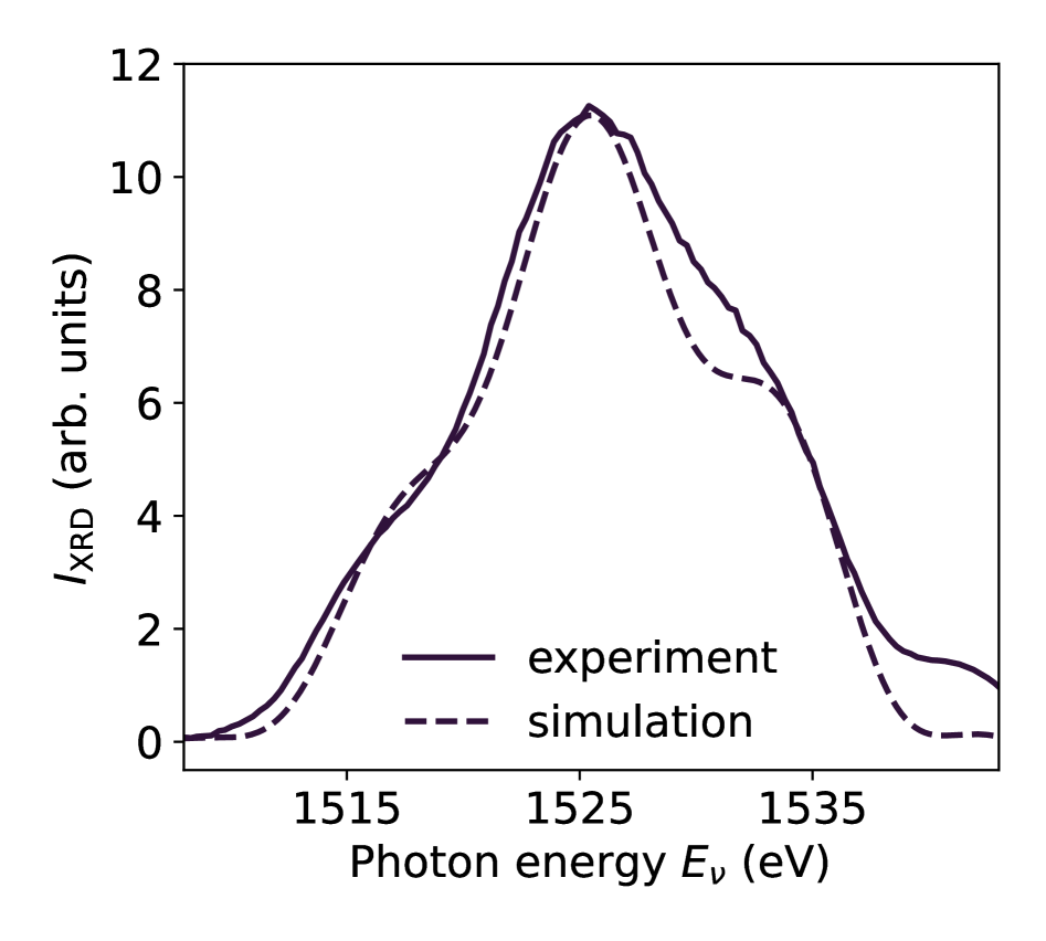
From , we calculated for each unit cell along and subsequently the diffraction profiles in the range (Figure S21d). A selection of diffraction curves at different (Figure S21e) are then compared to the experimental data (Figure S21f). The main features of the experimental data, i.e., the shift of the diffraction peak to smaller photon energies, the relative increase/decrease of the diffraction intensity on the low/high photon energy side, the larger broadening and smaller peak diffraction intensity as increases, are all well reproduced by our simulations. This strongly corroborates the validity of the model employed to describe our data. The initial shift to higher photon energy for is clearly shown by the increase of spectral weight around in Figure S21d. Conversely, for , the average positive strain explains the peak shift to lower photon energy, and the strain gradient is the reason for the change in spectral weight from the high to the low energy side. At the same time, a larger strain gradient leads to broader diffraction curves, and given the conservation of the total area under the curve, to a smaller peak intensity. Qualitatively, the simulated diffraction curves show sharper oscillations, related to the small film thickness, as compared to the experimental ones (Figure S21e-f). This is the consequence of a slightly larger broadening of the experimental curves that we assign to an initial strain profile , while we assume throughout the sample for the simulated curves (Figure S24). Finally, the discussion above regarding the incident pump fluence applies also to the lower fluence . Also in the latter case, we find an excellent agreement between experiments and simulations (Figure S22e-f).
Supplementary Note 10 Estimation of the bandgap decrease
To estimate the largest bandgap decrease, first we determine the photoinduced electronic pressure as [4], where [87] is the Grüneisen parameter, is the electronic heat capacity (Table S2), and is the largest increase in electronic temperature of the BTO film averaged over (Figure S17). Second, we express the bandgap variation as , where (Table S3).
Supplementary Note 11 Estimation of the electronic contribution to the ferroelectric polarization
To quantify the relative contribution of structural () and electronic () changes to the total polarization variation out of equilibrium , we first estimate , and then derive the relative magnitude of the electronic contribution . From polarization-electric field hysteresis loops on differently strained BTO thin films grown on a GSO substrate [26], the relative change of the polarization as a function of the strain was determined to be . In our data, at short time delays () the strain experiences a marginal change and is clearly dominated by the presence of photoexcited carriers in the conduction band (Figure 2e-f). At larger time delays (), reaches the saturation value of , which would correspond to an increase in polarization of (), assuming a polarization at equilibrium of as found for BTO/SRO/GSO [26]. In contrast, we measure an overall polarization change of (Figure 2e). As a result, it follows that the electronic contribution , responsible for the reduced polarization, has larger magnitude than the structural one even at ().
References
- [1] Martin, L. W. & Rappe, A. M. Thin-film ferroelectric materials and their applications. \JournalTitleNat. Rev. Mater. 2, 16087, DOI: 10.1038/natrevmats.2016.87 (2017).
- [2] Kim, I. & Lee, J. Ferroelectric Transistors for Memory and Neuromorphic Device Applications. \JournalTitleAdv. Mater. 35, 2206864, DOI: 10.1002/adma.202206864 (2023).
- [3] Guo, J. et al. Recent Progress in Optical Control of Ferroelectric Polarization. \JournalTitleAdv. Opt. Mater. 9, 2002146, DOI: 10.1002/adom.202002146 (2021).
- [4] Ruello, P. & Gusev, V. E. Physical mechanisms of coherent acoustic phonons generation by ultrafast laser action. \JournalTitleUltrasonics 56, 21–35, DOI: 10.1016/j.ultras.2014.06.004 (2015).
- [5] Korff Schmising, C. v. et al. Coupled Ultrafast Lattice and Polarization Dynamics in Ferroelectric Nanolayers. \JournalTitlePhys. Rev. Lett. 98, 257601, DOI: 10.1103/PhysRevLett.98.257601 (2007).
- [6] Schick, D. et al. Ultrafast lattice response of photoexcited thin films studied by X-ray diffraction. \JournalTitleStruct. dyn. 1, 064501, DOI: 10.1063/1.4901228 (2014).
- [7] Sheu, Y. M. et al. Using ultrashort optical pulses to couple ferroelectric and ferromagnetic order in an oxide heterostructure. \JournalTitleNat. Commun. 5, 1–6, DOI: 10.1038/ncomms6832 (2014).
- [8] Lee, H. J. et al. Structural Evidence for Ultrafast Polarization Rotation in Ferroelectric/Dielectric Superlattice Nanodomains. \JournalTitlePhys. Rev. X 11, 031031, DOI: 10.1103/PhysRevX.11.031031 (2021).
- [9] Li, T. et al. Optical control of polarization in ferroelectric heterostructures. \JournalTitleNat. Commun. 9, 3344, DOI: 10.1038/s41467-018-05640-4 (2018).
- [10] Ron, A. et al. Transforming a strain-stabilized ferroelectric into an intrinsic polar metal with light. \JournalTitlePhys. Rev. B 108, 224308, DOI: 10.1103/PhysRevB.108.224308 (2023).
- [11] Sarott, M. F. et al. Reversible Optical Control of Polarization in Epitaxial Ferroelectric Thin Films. \JournalTitleAdv. Mater. 36, 2312437, DOI: 10.1002/adma.202312437 (2024).
- [12] Daranciang, D. et al. Ultrafast Photovoltaic Response in Ferroelectric Nanolayers. \JournalTitlePhys. Rev. Lett. 108, 087601, DOI: 10.1103/PhysRevLett.108.087601 (2012).
- [13] Wen, H. et al. Electronic Origin of Ultrafast Photoinduced Strain in BiFeO3. \JournalTitlePhys. Rev. Lett. 110, 037601, DOI: 10.1103/PhysRevLett.110.037601 (2013).
- [14] Schick, D. et al. Localized Excited Charge Carriers Generate Ultrafast Inhomogeneous Strain in the Multiferroic BiFeO3. \JournalTitlePhys. Rev. Lett. 112, 097602, DOI: 10.1103/PhysRevLett.112.097602 (2014).
- [15] Matzen, S. et al. Tuning Ultrafast Photoinduced Strain in Ferroelectric-Based Devices. \JournalTitleAdv. Electron. Mater. 5, 1800709, DOI: 10.1002/aelm.201800709 (2019).
- [16] Ahn, Y. et al. Dynamic Tilting of Ferroelectric Domain Walls Caused by Optically Induced Electronic Screening. \JournalTitlePhys. Rev. Lett. 127, 097402, DOI: 10.1103/PhysRevLett.127.097402 (2021).
- [17] Sri Gyan, D. et al. Optically Induced Picosecond Lattice Compression in the Dielectric Component of a Strongly Coupled Ferroelectric/Dielectric Superlattice. \JournalTitleAdv. Electron. Mater. 8, 2101051, DOI: 10.1002/aelm.202101051 (2022).
- [18] Gu, R. et al. Temporal and spatial tracking of ultrafast light-induced strain and polarization modulation in a ferroelectric thin film. \JournalTitleSci. Adv. 9, DOI: 10.1126/sciadv.adi1160 (2023).
- [19] Ganguly, S. et al. Photostrictive Actuators Based on Freestanding Ferroelectric Membranes. \JournalTitleAdv. Mater. 36, 2310198, DOI: 10.1002/adma.202310198 (2024).
- [20] Chen, F. et al. Ultrafast terahertz-field-driven ionic response in ferroelectric BaTiO3. \JournalTitlePhys. Rev. B 94, 180104, DOI: 10.1103/PhysRevB.94.180104 (2016).
- [21] Mankowsky, R., von Hoegen, A., Först, M. & Cavalleri, A. Ultrafast Reversal of the Ferroelectric Polarization. \JournalTitlePhys. Rev. Lett. 118, 197601, DOI: 10.1103/PhysRevLett.118.197601 (2017).
- [22] Yang, Y., Paillard, C., Xu, B. & Bellaiche, L. Photostriction and elasto-optic response in multiferroics and ferroelectrics from first principles. \JournalTitleJ. Phys.: Condens. Matter 30, 073001, DOI: 10.1088/1361-648X/aaa51f (2018).
- [23] Devonshire, A. XCVI. Theory of barium titanate: Part I. \JournalTitleThe London, Edinburgh, and Dublin Philosophical Magazine and Journal of Science 40, 1040–1063, DOI: 10.1080/14786444908561372 (1949).
- [24] Choi, K. J. et al. Enhancement of Ferroelectricity in Strained BaTiO3 Thin Films. \JournalTitleScience 306, 1005–1009, DOI: 10.1126/science.1103218 (2004).
- [25] Dawber, M. et al. Tailoring the Properties of Artificially Layered Ferroelectric Superlattices. \JournalTitleAdv. Mater. 19, 4153–4159, DOI: 10.1002/adma.200700965 (2007).
- [26] Pesquera, D. et al. Beyond Substrates: Strain Engineering of Ferroelectric Membranes. \JournalTitleAdvanced Materials 32, 2003780, DOI: 10.1002/adma.202003780 (2020).
- [27] Zhang, Y. et al. Probing Ultrafast Dynamics of Ferroelectrics by Time-Resolved Pump-Probe Spectroscopy. \JournalTitleAdv. Sci. 8, 2102488, DOI: 10.1002/advs.202102488 (2021).
- [28] Chernova, E. et al. Strain-controlled optical absorption in epitaxial ferroelectric BaTiO films. \JournalTitleAppl. Phys. Lett. 106, 192903, DOI: 10.1063/1.4921083 (2015).
- [29] Lian, C., Ali, Z. A., Kwon, H. & Wong, B. M. Indirect but Efficient: Laser-Excited Electrons Can Drive Ultrafast Polarization Switching in Ferroelectric Materials. \JournalTitleJ. Phys. Chem. Lett. 10, 3402–3407, DOI: 10.1021/acs.jpclett.9b01046 (2019).
- [30] Chen, J., Hong, L., Huang, B. & Xiang, H. Ferroelectric switching assisted by laser illumination. \JournalTitlePhys. Rev. B 109, 094102, DOI: 10.1103/PhysRevB.109.094102 (2024).
- [31] Koleżyński, A. & Tkacz-Śmiech, K. From the Molecular Picture to the Band Structure of Cubic and Tetragonal Barium Titanate. \JournalTitleFerroelectrics 314, 123–134, DOI: 10.1080/00150190590926300 (2005).
- [32] Wright, O. B. & Gusev, V. E. Acoustic generation in crystalline silicon with femtosecond optical pulses. \JournalTitleAppl. Phys. Lett. 66, 1190–1192, DOI: 10.1063/1.113853 (1995).
- [33] Khenata, R. et al. First-principle calculations of structural, electronic and optical properties of BaTiO and BaZrO under hydrostatic pressure. \JournalTitleSolid State Commun. 136, 120–125, DOI: 10.1016/j.ssc.2005.04.004 (2005).
- [34] Chen, L. Y. et al. Ultrafast photoinduced mechanical strain in epitaxial BiFeO3 thin films. \JournalTitleAppl. Phys. Lett. 101, 041902, DOI: 10.1063/1.4734512 (2012).
- [35] Jin, Z. et al. Structural dependent ultrafast electron-phonon coupling in multiferroic BiFeO3 films. \JournalTitleAppl. Phys. Lett. 100, 071105, DOI: 10.1063/1.3685496 (2012).
- [36] Sheu, Y. M. et al. Ultrafast carrier dynamics and radiative recombination in multiferroic BiFeO3. \JournalTitleAppl. Phys. Lett. 100, 242904, DOI: 10.1063/1.4729423 (2012).
- [37] Wang, K. et al. Coupling Among Carriers and Phonons in Femtosecond Laser Pulses Excited SrRuO: A Promising Candidate for Optomechanical and Optoelectronic Applications. \JournalTitleACS Appl. Nano Mater. 2, 3882–3888, DOI: 10.1021/acsanm.9b00728 (2019).
- [38] Mudiyanselage, R. R. H. H. et al. Coherent acoustic phonons and ultrafast carrier dynamics in heteroepitaxial BaTiO3–BiFeO3 films and nanorods. \JournalTitleJ. Mater. Chem. C 7, 14212–14222, DOI: 10.1039/C9TC01584A (2019).
- [39] Denev, S. A., Lummen, T. T. A., Barnes, E., Kumar, A. & Gopalan, V. Probing Ferroelectrics Using Optical Second Harmonic Generation. \JournalTitleJ. Am. Ceram. Soc. 94, 2699–2727, DOI: 10.1111/j.1551-2916.2011.04740.x (2011).
- [40] Murgan, R., Tilley, D. R., Ishibashi, Y., Webb, J. F. & Osman, J. Calculation of nonlinear-susceptibility tensor components in ferroelectrics: cubic, tetragonal, and rhombohedral symmetries. \JournalTitleJ. Opt. Soc. Am. B 19, 2007, DOI: 10.1364/JOSAB.19.002007 (2002).
- [41] Thomsen, C., Grahn, H. T., Maris, H. J. & Tauc, J. Surface generation and detection of phonons by picosecond light pulses. \JournalTitlePhys. Rev. B 34, 4129–4138, DOI: 10.1103/PhysRevB.34.4129 (1986).
- [42] Young, E. S. K., Akimov, A. V., Campion, R. P., Kent, A. J. & Gusev, V. Picosecond strain pulses generated by a supersonically expanding electron-hole plasma in GaAs. \JournalTitlePhys. Rev. B 86, 155207, DOI: 10.1103/PhysRevB.86.155207 (2012).
- [43] Gattinoni, C. et al. Interface and surface stabilization of the polarization in ferroelectric thin films. \JournalTitlePNAS 117, 28589–28595, DOI: 10.1073/pnas.2007736117 (2020).
- [44] Wang, Y., Liu, X., Burton, J. D., Jaswal, S. S. & Tsymbal, E. Y. Ferroelectric Instability Under Screened Coulomb Interactions. \JournalTitlePhys. Rev. Lett. 109, 247601, DOI: 10.1103/PhysRevLett.109.247601 (2012).
- [45] Paillard, C., Torun, E., Wirtz, L., Íñiguez, J. & Bellaiche, L. Photoinduced Phase Transitions in Ferroelectrics. \JournalTitlePhys. Rev. Lett. 123, 087601, DOI: 10.1103/PhysRevLett.123.087601 (2019).
- [46] Fridkin, V. M. Bulk photovoltaic effect in noncentrosymmetric crystals. \JournalTitleCrystallogr. Rep. 46, 654–658, DOI: 10.1134/1.1387133 (2001).
- [47] Dai, Z. & Rappe, A. M. Recent progress in the theory of bulk photovoltaic effect. \JournalTitleChem. Phys. Rev. 4, 011303, DOI: 10.1063/5.0101513 (2023).
- [48] Matsuo, H. & Noguchi, Y. Bulk photovoltaic effect in ferroelectrics. \JournalTitleJpn. J. Appl. Phys. 63, 060101, DOI: 10.35848/1347-4065/ad442e (2024).
- [49] Koch, W. T. H., Munser, R., Ruppel, W. & Würfel, P. Bulk photovoltaic effect in BaTiO3. \JournalTitleSolid State Commun. 17, 847–850, DOI: 10.1016/0038-1098(75)90735-8 (1975).
- [50] Koch, W. T. H., Munser, R., Ruppel, W. & Würfel, P. Anomalous photovoltage in BaTiO3. \JournalTitleFerroelectrics 13, 305–307, DOI: 10.1080/00150197608236596 (1976).
- [51] Kundys, B., Viret, M., Colson, D. & Kundys, D. O. Light-induced size changes in BiFeO3 crystals. \JournalTitleNat. Mater. 9, 803–805, DOI: 10.1038/nmat2807 (2010).
- [52] Young, S. M. & Rappe, A. M. First Principles Calculation of the Shift Current Photovoltaic Effect in Ferroelectrics. \JournalTitlePhys. Rev. Lett. 109, 116601, DOI: 10.1103/PhysRevLett.109.116601 (2012).
- [53] Sanna, S., Thierfelder, C., Wippermann, S., Sinha, T. P. & Schmidt, W. G. Barium titanate ground- and excited-state properties from first-principles calculations. \JournalTitlePhys. Rev. B 83, 054112, DOI: 10.1103/PhysRevB.83.054112 (2011).
- [54] Paillard, C., Xu, B., Dkhil, B., Geneste, G. & Bellaiche, L. Photostriction in Ferroelectrics from Density Functional Theory. \JournalTitlePhys. Rev. Lett. 116, 247401, DOI: 10.1103/PhysRevLett.116.247401 (2016).
- [55] Wen, Y.-C. et al. Efficient generation of coherent acoustic phonons in (111) InGaAs/GaAs multiple quantum wells through piezoelectric effects. \JournalTitleApplied Physics Letters 90, 172102, DOI: 10.1063/1.2731441 (2007).
- [56] Li, T., Deng, S., Liu, H. & Chen, J. Insights into Strain Engineering: From Ferroelectrics to Related Functional Materials and Beyond. \JournalTitleChem. Rev. 124, 7045–7105, DOI: 10.1021/acs.chemrev.3c00767 (2024).
- [57] Zhao, T., Lu, H., Chen, F., Yang, G. & Chen, Z. Stress-induced enhancement of second-order nonlinear optical susceptibilities of barium titanate films. \JournalTitleJ. Appl. Phys. 87, 7448–7451, DOI: 10.1063/1.373008 (2000).
- [58] Jeong, J.-W., Shin, S.-C., Lyubchanskii, I. L. & Varyukhin, V. N. Strain-induced three-photon effects. \JournalTitlePhys. Rev. B 62, 13455–13463, DOI: 10.1103/PhysRevB.62.13455 (2000).
- [59] Birkholz, M. Thin Film Analysis by X-Ray Scattering (Wiley-VCH, Weinheim, 2005).
- [60] Young, R. A. & Wiles, D. B. Profile shape functions in Rietveld refinements. \JournalTitleJ. Appl. Crystallogr. 15, 430–438, DOI: https://doi.org/10.1107/S002188988201231X (1982).
- [61] Rodriguez, B. J., Callahan, C., Kalinin, S. V. & Proksch, R. Dual-frequency resonance-tracking atomic force microscopy. \JournalTitleNanotechnology 18, 475504, DOI: https://doi.org/10.1088/0957-4484/18/47/475504 (2007).
- [62] Löhl, F. et al. Electron Bunch Timing with Femtosecond Precision in a Superconducting Free-Electron Laser. \JournalTitlePhys. Rev. Lett. 104, 144801, DOI: 10.1103/PhysRevLett.104.144801 (2010).
- [63] Czwalinna, M. et al. Beam Arrival Stability at the European XFEL. \JournalTitleProceedings of the 12th International Particle Accelerator Conference IPAC2021 (2021).
- [64] Carley, R., Van Kuiken, B., Le Guyader, L., Mercurio, G. & Scherz, A. (eds.) SCS Instrument Review Report (European X-Ray Free-Electron Laser Facility GmbH, Schenefeld, 2022).
- [65] Schneidmiller, E. A. & Yurkov, M. V. Photon beam properties at the European XFEL (December 2010 revision). \JournalTitleTESLA-FEL 2010-06 127 (2010).
- [66] Gerasimova, N. et al. The soft X-ray monochromator at the SASE3 beamline of the European XFEL: from design to operation. \JournalTitleJ. Synchrotron Radiat. 29, 1299–1308, DOI: 10.1107/S1600577522007627 (2022).
- [67] Zhang, Y. et al. Characterization of domain distributions by second harmonic generation in ferroelectrics. \JournalTitleNpj Comput. Mater. 4, 39, DOI: 10.1038/s41524-018-0095-6 (2018).
- [68] Thompson, J. et al. Enhanced metallic properties of SrRuO thin films via kinetically controlled pulsed laser epitaxy. \JournalTitleAppl. Phys. Lett. 109, 161902, DOI: 10.1063/1.4964882 (2016).
- [69] Yamanaka, S. et al. Thermophysical properties of SrHfO3 and SrRuO3. \JournalTitleJ. Solid State Chem. 177, 3484–3489, DOI: 10.1016/j.jssc.2004.05.039 (2004).
- [70] Hidde, J., Guguschev, C., Ganschow, S. & Klimm, D. Thermal conductivity of rare-earth scandates in comparison to other oxidic substrate crystals. \JournalTitleJ. Alloys Compd. 738, 415–421, DOI: 10.1016/j.jallcom.2017.12.172 (2018).
- [71] de Jong, M. et al. Charting the complete elastic properties of inorganic crystalline compounds. \JournalTitleSci. Data 2, 150009, DOI: 10.1038/sdata.2015.9 (2015).
- [72] Mills, I., International Union of Pure and Applied Chemistry & International Union of Pure and Applied Chemistry (eds.) Quantities, units, and symbols in physical chemistry (1993), 2nd ed edn.
- [73] He, Y. Heat capacity, thermal conductivity, and thermal expansion of barium titanate-based ceramics. \JournalTitleThermochim. Acta 419, 135–141, DOI: 10.1016/j.tca.2004.02.008 (2004).
- [74] Anisimov, S. I., Kapeliovich, B. L. & Perelman, T. L. Electron emission from metal surfaces exposed to ultrashort laser pulses. \JournalTitleZh. Eksp. Teor. Fiz 66, 375–7 (1974).
- [75] Müller, A. & Härdtl, K. H. Ambipolar diffusion phenomena in BaTiO and SrTiO. \JournalTitleAppl. Phys. A 49, 75–82, DOI: 10.1007/BF00615468 (1989).
- [76] Wang, Z., Yang, M. & Zhang, H. Strain engineering on electrocaloric effect in PbTiO and BaTiO. \JournalTitleAdv. Compos. Hybrid Mater. 4, 1239–1247, DOI: 10.1007/s42114-021-00257-6 (2021).
- [77] de Ligny, D. & Richet, P. High-temperature heat capacity and thermal expansion of SrTiO3 and SrZrO3 perovskites. \JournalTitlePhys. Rev. B 53, 3013–3022, DOI: 10.1103/PhysRevB.53.3013 (1996).
- [78] Guyot, F., Richet, P., Courtial, P. & Gillet, P. High-temperature heat capacity and phase transitions of CaTiO perovskite. \JournalTitlePhys. Chem. Miner. 20 (1993).
- [79] Vladimirov, V. S. (ed.) A Collection of Problems on the Equations of Mathematical Physics (Springer Berlin Heidelberg, Berlin, Heidelberg, 1986).
- [80] Lin, Z., Zhigilei, L. V. & Celli, V. Electron-phonon coupling and electron heat capacity of metals under conditions of strong electron-phonon nonequilibrium. \JournalTitlePhys. Rev. B 77, 075133, DOI: 10.1103/PhysRevB.77.075133 (2008).
- [81] Wang, X. Y., Riffe, D. M., Lee, Y.-S. & Downer, M. C. Time-resolved electron-temperature measurement in a highly excited gold target using femtosecond thermionic emission. \JournalTitlePhys. Rev. B 50, 8016–8019, DOI: 10.1103/PhysRevB.50.8016 (1994).
- [82] Rumble, J. R. (ed.) CRC Handbook of Chemistry and Physics (CRC Press, 2023), 104th edn.
- [83] Fundamental Physical Constants from NIST.
- [84] Chan, C. C. S. et al. Uncovering the Electron-Phonon Interplay and Dynamical Energy-Dissipation Mechanisms of Hot Carriers in Hybrid Lead Halide Perovskites. \JournalTitleAdv. Energy Mater. 11, 2003071, DOI: 10.1002/aenm.202003071 (2021).
- [85] Elsayed-Ali, H. E., Norris, T. B., Pessot, M. A. & Mourou, G. A. Time-resolved observation of electron-phonon relaxation in copper. \JournalTitlePhys. Rev. Lett. 58, 1212–1215, DOI: 10.1103/PhysRevLett.58.1212 (1987).
- [86] Hohlfeld, J. et al. Electron and lattice dynamics following optical excitation of metals. \JournalTitleChem. Phys. 251, 237–258, DOI: 10.1016/S0301-0104(99)00330-4 (2000).
- [87] Choithrani, R. Structural, elastic and thermal properties of batio3. \JournalTitleInvertis Journal of Science & Technology 7, 72–77 (2014).