Revisiting DRAM Read Disturbance: Identifying Inconsistencies
Between Experimental Characterization and
Device-Level Studies
Abstract
Modern DRAM is vulnerable to read disturbance (e.g., RowHammer and RowPress) that significantly undermines the robust operation of the system. Repeatedly opening and closing a DRAM row (RowHammer) or keeping a DRAM row open for a long period of time (RowPress) induces bitflips in nearby unaccessed DRAM rows. Prior works on DRAM read disturbance either 1) perform experimental characterization using commercial-off-the-shelf (COTS) DRAM chips to demonstrate the high-level characteristics of the read disturbance bitflips, or 2) perform device-level simulations to understand the low-level error mechanisms of the read disturbance bitflips.
In this paper, we attempt to align and cross-validate the real-chip experimental characterization results and state-of-the-art device-level studies of DRAM read disturbance. To do so, we first identify and extract the key bitflip characteristics of RowHammer and RowPress from the device-level error mechanisms studied in prior works. Then, we perform experimental characterization on 96 COTS DDR4 DRAM chips that directly match the data and access patterns studied in the device-level works. Through our experiments, we identify fundamental inconsistencies in the RowHammer and RowPress bitflip directions and access pattern dependence between experimental characterization results and the device-level error mechanisms.
Based on our results, we hypothesize that either 1) the retention failure based DRAM architecture reverse-engineering methodologies do not fully work on modern DDR4 DRAM chips, or 2) existing device-level works do not fully uncover all the major read disturbance error mechanisms. We hope our findings inspire and enable future works to build a more fundamental and comprehensive understanding of DRAM read disturbance.
1 Introduction
Memory isolation is critical to ensure the robust (i.e., safe, secure, and reliable) operation of modern computing systems. Accessing a memory address should not have unintended side-effects on data stored in other unaccessed memory addresses. Unfortunately, dynamic random access memory (DRAM) [1], the major main memory technology, suffers from read disturbance (e.g., RowHammer and RowPress) [2, 3, 4, 5, 6, 7, 8, 9, 10, 11, 12, 13, 14, 15], i.e., repeatedly opening and closing a DRAM row (RowHammer) or keeping a DRAM row open for a long period of time (RowPress) induces bitflips in nearby unaccessed DRAM rows. DRAM read disturbance is a critical security vulnerability as attackers can induce and exploit RowHammer and RowPress bitflips to take over a system or leak private or security-critical data [16, 17, 18, 19, 20, 21, 22, 23, 24, 2, 25, 26, 27, 28, 29, 30, 31, 32, 33, 34, 35, 36, 37, 8, 38, 39, 40, 41, 42, 43, 44, 9, 45, 46, 47, 48, 49, 50, 51, 52, 53, 54, 55, 56, 57, 58, 59, 60, 61, 62, 63, 64, 65, 10, 66, 67, 68, 69, 70, 71, 72]. Therefore, to make DRAM-based main memory more robust (i.e., safer, more secure, and more reliable), it is important to rigorously study and understand read disturbance mechanisms like RowHammer and RowPress.
Prior works on DRAM read disturbance either 1) perform experimental characterization using commercial-off-the-shelf (COTS) DRAM chips [2, 3, 4, 5, 6, 7, 8, 9, 10, 11, 12, 13, 14, 15] to demonstrate the high-level characteristics of the read disturbance bitflips, or 2) perform device-level simulations to understand the low-level error mechanisms that induce the bitflips [73, 74, 75, 76, 77, 78, 79]. Unfortunately, observations from experimental characterization works do not always match the device-level phenomena because the DRAM architecture and array layout is not visible from the DRAM chip-level. For example, a DRAM cell can represent a logical “1” value by either having (i.e., a true-cell) or (i.e., an anti-cell) at the storage node (vice versa for representing a logical “0”) [80]. Thus, observing a “1” to “0” bitflip through experimental characterization of COTS DRAM chips does not always mean a DRAM cell’s storage node voltage drops from .
Our goal in this paper is to align and cross-validate the experimental characterization of read disturbance with the low-level fundamental error mechanisms modeled by device-level simulation works. We do so by comparing two fundamental properties of the read disturbance bitflips: 1) bitflip direction, and 2) the dependence on DRAM cell data pattern and DRAM row access pattern. To do so, we first identify and extract the key first-order read disturbance error-mechanisms from state-of-the-art device-level works [73, 74, 75, 76, 77, 78, 79], and then perform experimental characterization of DRAM read disturbance on 96 COTS DDR4 DRAM chips from all three major manufacturers (Samsung, SK Hynix, and Micron) using DRAM Bender [81, 82] 1) that directly match the data and access patterns studied in device-level works, and 2) apply state-of-the-art DRAM architecture and true- and anti-cell layout reverse engineering techniques based on DRAM cell retention failures [80, 83, 84, 85, 86, 7] to try to match the characterization results to device-level phenomena.
We identify the following key inconsistencies between experimental characterization and state-of-the-art proposed device-level mechanisms:
-
•
For double-sided RowHammer, experimental characterization shows bitflips in both directions (“1” to “0” and “0” to “1”) while device-level mechanisms suggest only “1” to “0” bitflips will happen.
-
•
For double-sided RowHammer, experimental characterization shows that “0” to “1” bitflips appear first while device-level mechanisms suggest the error mechanism to induce “1” to “0” bitflips is significantly stronger than “0” to “1” bitflips.
-
•
For single-sided RowPress, experimental characterization shows overwhelmingly “1” to “0” bitflips while device-level mechanisms suggest both kinds of bitflips will happen.
Based on our results, we hypothesize that either 1) existing device-level works do not fully uncover all the major read disturbance error mechanisms, or 2) existing retention-failure-based DRAM architecture reverse-engineering methodologies do not fully work on modern DDR4 DRAM chips. We hope that our findings enable future works to build a more fundamental and comprehensive understanding of DRAM read disturbance.
We make the following contributions in this paper:
-
•
To our knowledge, this is the first paper to systematically demonstrate the fundamental inconsistencies of DRAM read disturbance bitflip characteristics between real-chip experimental characterization and proposed device-level error mechanisms.
-
•
The observations from our experimental characterization provides insights for future works to build a more fundamental and comprehensive understanding of DRAM read disturbance.
-
•
We open source [87] all our experimental infrastructure, code, and data to facilitate future research on DRAM read disturbance.
2 Background
We provide a brief explanation on 1) the logical organization and key operations of DRAM-based main memory, 2) the physical structure of a DRAM cell, and 3) the DRAM read disturbance phenomenon and the key read disturbance bitflip characteristics modeled by state-of-the-art device-level TCAD simulation works.
2.1 DRAM-Based Main Memory
Figure 1 illustrates the logical organization of modern DRAM-based main memory. The CPU’s memory controller controls a memory channel that one or more DRAM modules connect to. A module contains one or multiple DRAM ranks that share the memory channel. A rank is made up of multiple DRAM chips that operate in lock-step. Each DRAM chip contains multiple DRAM banks that can be accessed independently.
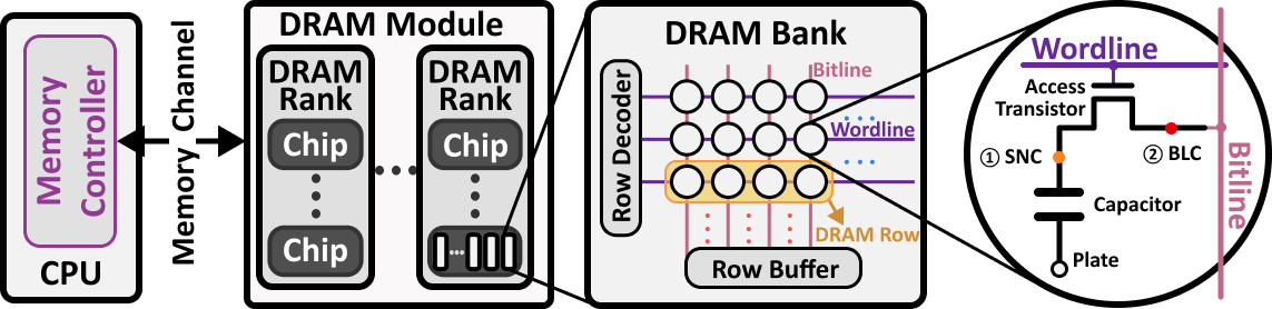
In a DRAM bank, DRAM cells are organized in a 2D array addressed by rows (wordlines) and columns (bitlines). A DRAM cell stores one bit of information in the form of electric charge in its capacitor. The capacitor is connected to the bitline through the access transistor, controlled by the wordline. The other end of the capacitor is connected to a constant voltage source (plate, usually ) to reduce the stress of the electric field across the capacitor [88, 89].
To access DRAM, the memory controller first sends an ACT (activate) command with a row address that 1) opens a DRAM row in a bank, and 2) transfers the data stored in the DRAM cells to the row buffer (i.e., bitline sense amplifiers, BLSA). Second, the memory controller sends a RD/WR command with a column address to read or write the desired data in the row buffer. Third, to prepare the DRAM bank for subsequent accesses to other DRAM rows, the memory controller sends a PRE (precharge) command to close the opened DRAM row and reset the row buffer for the next accesses.
Because the BLSA is essentially a cross-coupled pair of inverters, a DRAM cell can represent either a logical “1” as storing positive charge (i.e., true-cell) or storing negative charge (i.e., anti-cell), depending on which side of the BLSA its bitline is connected to (vice versa for representing a logical “0”) [80, 83, 7].
2.2 Physical DRAM Cell Structure
Figure 2.a illustrates the physical layout of modern high-density open-bitline DRAM cell array. The capacitor of a DRAM cell is connected to an active region (i.e., the area where transistors are formed) through the storage node contact (SNC, ① in Figure 1 and Figure 2). Two DRAM cells belonging to two neighboring wordlines (rows) are fabricated in the same active region, and they share the same bitline contact (BLC, ② in Figure 1 and Figure 2).
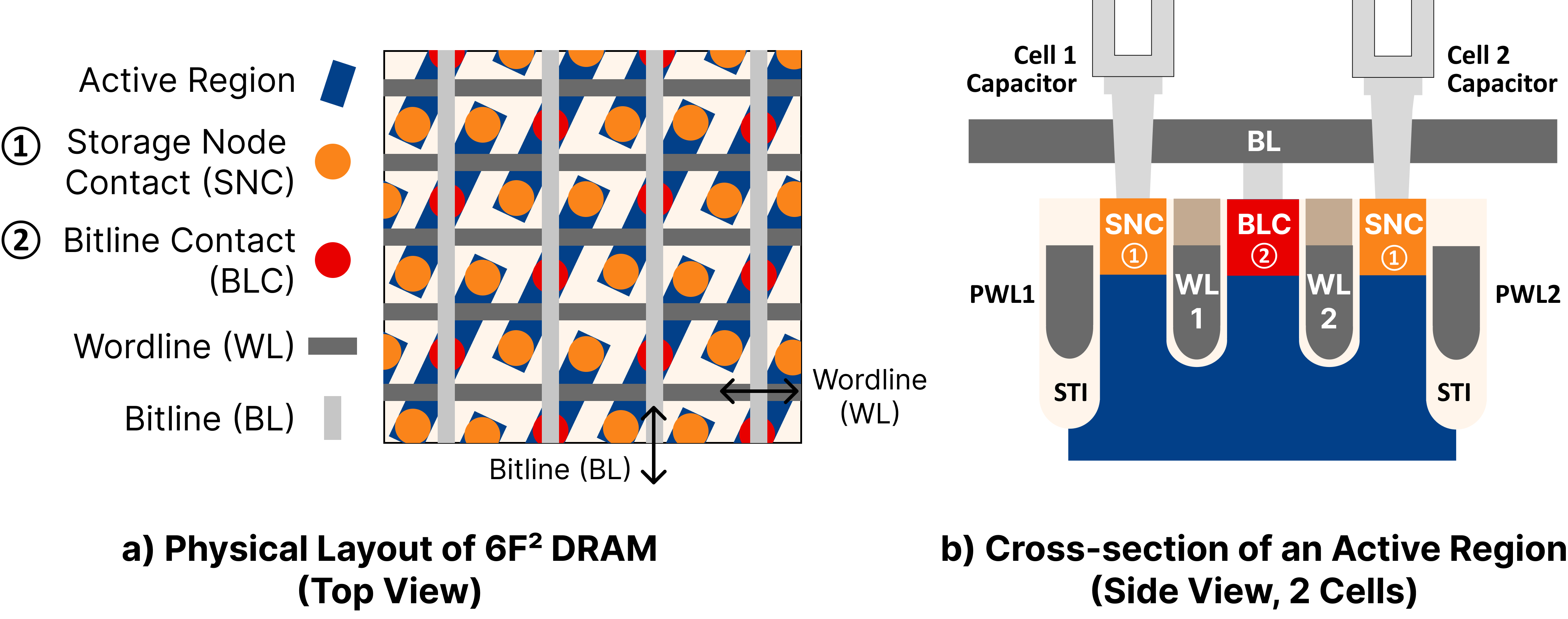
Figure 2.b shows the physical structure of DRAM cells using a side view of a cross section of an active region containing two cells. For any DRAM cell (e.g., Cell 1 in Figure 2.b), two other wordlines are in close proximity that can become potential aggressor rows to induce DRAM read disturbance: 1) the neighboring wordline (NWL) that controls the other DRAM cell in the same active region (i.e., WL2, Cell 2’s wordline), and 2) the passing wordline (PWL) in the shallow trench isolation (STI) region that does not form an access transistor in the active region (i.e., PWL1).
2.3 DRAM Read Disturbance
DRAM read disturbance is the phenomenon that accessing a DRAM row (aggressor row) disturbs the data stored in nearby unaccessed rows (victim rows). Prior works [2, 3, 4, 5, 6, 7, 8, 9, 10, 11, 12, 13, 14, 15] demonstrate that DRAM is vulnerable to two types of read disturbance phenomena, RowHammer [2, 3, 4, 5, 8, 9, 10, 13, 14, 15] and RowPress [6, 7, 11, 12, 14, 15].
RowHammer. RowHammer is a read disturbance phenomenon where repeatedly opening (activating) and closing the aggressor DRAM row many times (e.g., tens of thousands of times [3, 4]) causes bitflips in the victim rows.
RowPress. RowPress is a read disturbance phenomenon where keeping the aggressor row open for a long period of time causes bitflips in victim row. Doing so requires much fewer aggressor row activations to cause bitflips compared to RowHammer (i.e., orders of magnitude reduction [6, 12]).
In the next section, we 1) summarize the fundamental error mechanisms modeled and studied in state-of-the-art device-level research on DRAM read disturbance [73, 74, 75, 76, 77, 78, 79], and 2) identify the key read disturbance bitflip characteristics based on the most fundamental and dominating device-level error mechanisms studied in prior works.
3 Device-Level Mechanisms from Prior Works
3.1 Key Error Mechanisms of RowHammer
When only the neighboring wordline (NWL, i.e., the wordline that shares the same active region with the victim DRAM cell) is the aggressor row in RowHammer, trap-assisted electron migration is the major error mechanism for RowHammer [74, 75, 76]. The charge traps near the NWL silicon/gate interface are filled with electrons when NWL is activated. These electrons then get released when NWL is closed, and some of them migrate to the victim storage node causing a “1” to “0” leakage. When only the passing wordline (i.e., PWL) is the aggressor row in RowHammer, the passing gate effect [90, 76, 7] pulls electrons away from the storage node of the victim, causing a “0” to “1” leakage.
For double-sided RowHammer (i.e., when both NWL and PWL are activated in an alternating access pattern), the trap-assisted electron migration mechanism is significantly enhanced because PWL is open when NWL is off [76]. The electric field from the open PWL significantly enhances the migration of the electrons from traps near NWL to the victim node during the off-phase of the NWL, causing a significantly stronger “1” to “0” leakage. [76] further claims “0” to “1” bitflips are “eliminated completely”. Assuming this is indeed the major error mechanism for double-sided RowHammer, then the bitflips that manifest should have the following characteristics.
| Characteristic 1. Double-sided RowHammer should induce only “1” to “0” bitflips. |
3.2 Key Error Mechanisms of RowPress
When the NWL aggressor is open for a long period of time, more electrons are drawn from the victim storage node to the BLC, causing a stronger “0” to “1” leakage [79, 77]. When the PWL aggressor is open for a long period of time, it draws more electrons towards the direction of the victim storage node, causing a stronger “1” to “0” leakage[79, 77].
| Characteristic 2. Single-sided RowPress should induce both “1” to “0” and “0” to “1” bitflips. |
4 Experimental Testing Methodology
4.1 COTS DDR4 DRAM Testing Infrastructure
We use DRAM Bender [81, 91] (built over SoftMC [82, 92]), an FPGA-based COTS DDR4 DRAM testing infrastructure that gives us fine-grained control of DRAM commands and timings. The infrastructure consists of 1) a host PC that that generates the test program and collects experiment results, 2) an FPGA development board programmed with DRAM Bender that executes the test programs, and 3) the DRAM module under test that is connected to the FPGA board. We also attach a pair of heater pads controlled with a PID-based temperature controller [93] that can maintain and/or increase the temperature of the DRAM.
4.2 Reverse Engineering DRAM Array Architecture and Layout
In-DRAM Row Mapping. We apply the same methodology as prior works [53, 4, 5, 6, 7] that use single-sided RowHammer to identify the two neighboring rows of an aggressor row.
True- and Anti-Cell Layout. We apply the same methodology as prior work [7] that leverages DRAM retention failure to reverse engineer the layout of true- and anti-cells in DRAM based on the assumption that only a physical “1” will experience retention failures [80, 7]. We find that all the DRAM chips we test from Mfr. S and H have only true-cells, and DRAM chips from Mfr. M have true- and anti-cells interleaved at subarray granularity.111We also find that certain DRAM chips from Mfr. M have both true- and anti-cells within the same row. We do not include them in the study to simplify the testing.
4.3 COTS DDR4 DRAM Chips Tested
We test 12 different types of commercial-off-the-shelf (COTS) DDR4 DRAM chips (different die revisions and densities) from 12 modules (96 chips in total) from all three major DRAM manufacturers (Mfr. S, H, and M).222Our selection of DRAM modules to test is limited by two factors. First, we have access to only retail channels, which do not always offer all the DRAM die densities and revisions. Second, to make sure we can align experimental characterization results to device-level mechanisms, we need to ensure we reverse-engineer the DRAM array layout (e.g., row mapping and true- and anti-cell layout) of the DRAM chips we test. The array layout of many DRAM chips from Mfr. M are difficult to reverse-engineer, so we do not include them in the study to simplify testing. Table 1 lists all the DRAM chips we test. For every DRAM, we test 2048 rows in bank 1.333We assume no significant difference in read disturbance and retention failure characteristics across different banks. To save testing time, we test only bank 1.
| Mfr. | Module Type | Die Density | Die Revision | DQ | Num. Chips |
|
||
|---|---|---|---|---|---|---|---|---|
| S | UDIMM | 8 Gb | B | 8 | 8 | 1639 | ||
| S | UDIMM | 8 Gb | D | 8 | 8 | 2110 | ||
| S | UDIMM | 8 Gb | E | 8 | 8 | 2341 | ||
| S | UDIMM | 16 Gb | M | 8 | 8 | 2118 | ||
| S | UDIMM | 16 Gb | A | 8 | 8 | 2319 | ||
| S | UDIMM | 16 Gb | B | 8 | 8 | 2315 | ||
| S | UDIMM | 16 Gb | C | 8 | 8 | 2408 | ||
| H | UDIMM | 8 Gb | C | 8 | 8 | 2120 | ||
| H | UDIMM | 8 Gb | D | 8 | 8 | 1938 | ||
| H | UDIMM | 16 Gb | A | 8 | 8 | 2003 | ||
| H | UDIMM | 16 Gb | C | 8 | 8 | 2136 | ||
| M | UDIMM | 8 Gb | E | 8 | 8 | 2402 |
5 Experimental Characterization Results
5.1 HCFirst with Double-Sided RowHammer
Metric. To align the experimental characterization results with Characteristics 1, we first test the minimum aggressor row activation (hammer) count to induce at least one bitflip in the victim row, i.e., HCFirst, for both “0” to “1” and “1” to “0” bitflips. In double-sided RowHammer, we define HCFirst as the per-aggressor-row hammer count.
Methodology. To find HCFirst of a victim row, we sweep the range of possible hammer count values (bounded by the DDR4 DRAM refresh window of 64ms) from 0 to 500K with a step size of 1000 until we find at least one bitflip in the victim row. If we do not find bitflips within 500K hammers, we report we do not find a bitflip. We initialize the victim row with either all-zeros (0x00) or all-ones (0xFF), and initialize both aggressor rows with the opposite data of the victim row. We skip victim rows that do not have two neighboring rows (e.g., at subarray boundaries or are remapped due to repair). We keep the DRAM temperature constant at 50∘C.
Results. Figure 3 plots the distribution of the HCFirst values (y-axis) with both “0” to “1” (i.e., the victim row has data 0x00) and “1” to “0” (i.e., the victim row has data 0xFF) bitflips across all the victim rows we test for all types of DRAM chips we test in box and whiskers plots.444The box is bounded by the first quartile (i.e., the median of the first half of the ordered set of data points) and the third quartile (i.e., the median of the second half of the ordered set of data points). The whiskers represent the InterQuartile Range (IQR, the distance between the first and third quartiles, i.e., box size). The fliers represent outlier values. A lower HCFirst value means it is easier to induce bitflips since doing so needs fewer aggressor row activations. We make two observations from the results.
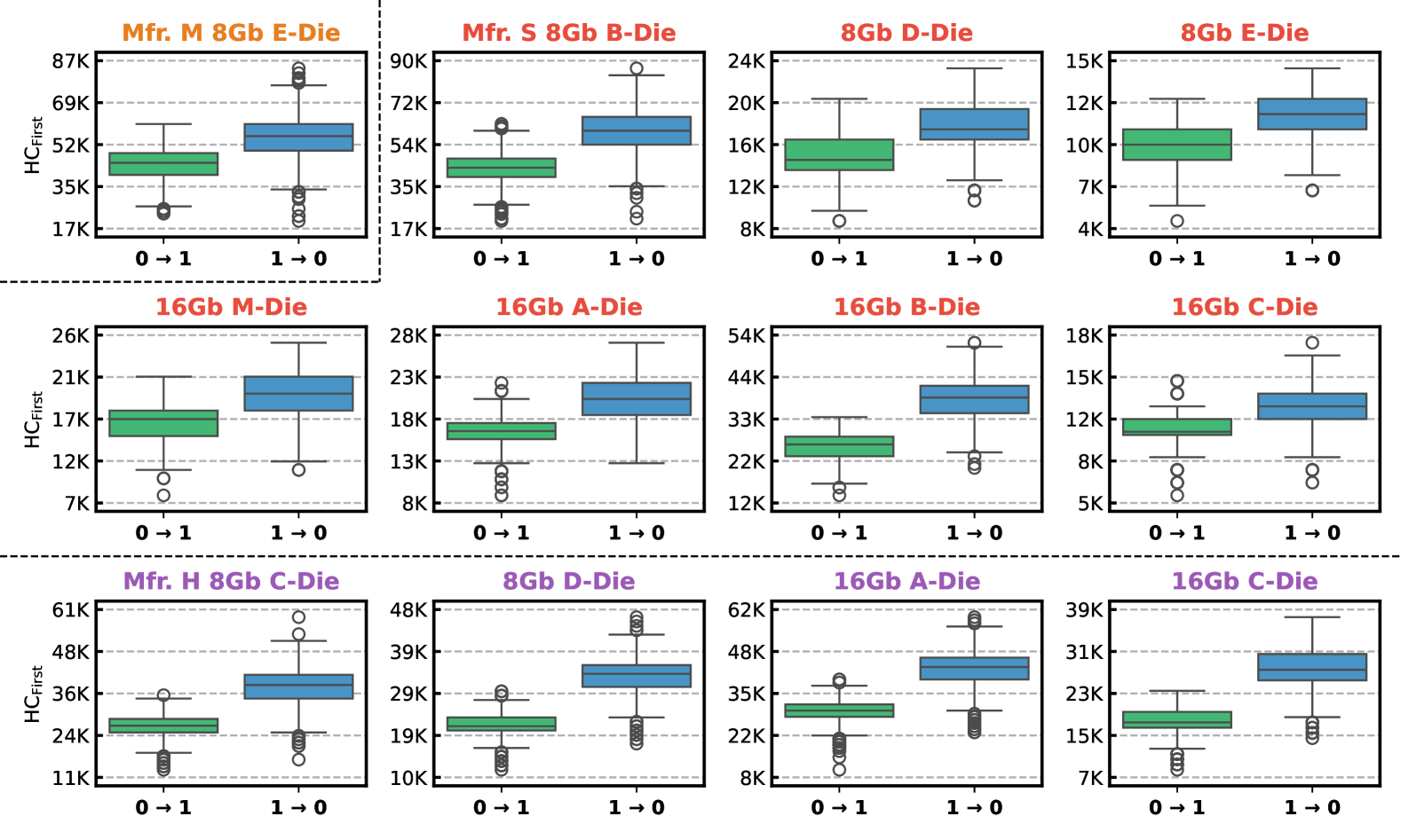
| Observation 1. Double-Sided RowHammer induces both “0” to “1” and “1” to “0” bitflips. |
We observe that, for all the DRAM chips we test, Double-Sided RowHammer induces both “0” to “1” and “1” to “0” bitflips. For the same victim DRAM row, we always observe both “0” to “1” and “1” to “0” bitflips.
| Observation 2. For Double-Sided RowHammer, the HCFirst values of “0” to “1” bitflips are significantly smaller than that of the “1” to “0” bitflips. |
We observe that, for all the DRAM chips we test, Double-Sided RowHammer induces “0” to “1” bitflips significantly more easily than it induces “1” to “0” bitflips. Table 2 lists the average HCFirst values of both “0” to “1” and “1” to “0” bitflips for all the DRAM chips we test. Across all DRAM chips we test, the average HCFirst of “0” to “1” bitflips is 24.7% smaller than the average HCFirst of “1” to “0” bitflips. This implies that the error mechanism for “0” to “1” bitflips is stronger than “1” to “0” bitflips in the most vulnerable DRAM cells.
| Mfr. | Die Density | Die Revision | Average HCFirst | Difference |
|
|||
|---|---|---|---|---|---|---|---|---|
| 0 to 1 | 1 to 0 | |||||||
| S | 8 Gb | B | 43840 | 59368 | 26.2% | 24.7% | ||
| S | 8 Gb | D | 15398 | 18041 | 14.7% | |||
| S | 8 Gb | E | 9684 | 11623 | 16.7% | |||
| S | 16 Gb | M | 16732 | 19946 | 16.1% | |||
| S | 16 Gb | A | 16981 | 20942 | 18.9% | |||
| S | 16 Gb | B | 26415 | 38774 | 31.9% | |||
| S | 16 Gb | C | 11355 | 13346 | 14.9% | |||
| H | 8 Gb | C | 26500 | 38440 | 31.1% | |||
| H | 8 Gb | D | 22069 | 33489 | 34.1% | |||
| H | 16 Gb | A | 29825 | 43326 | 31.2% | |||
| H | 16 Gb | C | 18042 | 28041 | 35.7% | |||
| M | 8 Gb | E | 44468 | 55605 | 20.0% | |||
We derive the following two key takeaways.
| Takeaway 1. Double-Sided RowHammer involves error mechanisms for inducing both “0” to “1” and “1” to “0” bitflips. |
| Takeaway 2. For Double-Sided RowHammer, the observed error mechanism for “0” to “1” bitflips is stronger than “1” to “0” bitflips in the most vulnerable DRAM cells (i.e., those requiring the least number of aggressor row activations to experience bitflips). |
5.2 Bitflip Count with Double-Sided RowHammer
Metric. To further investigate the bitflip characteristics of double-sided RowHammer, we test the maximum number of bitflips that can be induced within the refresh window (i.e., 64ms) for both “0” to “1” and “1” to “0” bitflips.
Methodology. To induce the maximum number of bitflips, we activate each aggressor row 500K times and then count the number of bitflips in the victim row. We initialize the victim row with either all-zeros (0x00) or all-ones (0xFF), and initialize both aggressor rows with the opposite data of the victim row. We skip victim rows that do not have two neighboring rows (e.g., at subarray boundaries or are remapped due to repair). We keep the DRAM temperature constant at 50∘C.
Results. Figure 4 plots the distribution of the number of bitflips per victim row (y-axis) with both “0” to “1” (i.e., the victim row has data 0x00) and “1” to “0” (i.e., the victim row has data 0xFF) bitflips (x-axis) for all types of DRAM chips we test in box and whiskers plots.4 We make the following observation from the results.
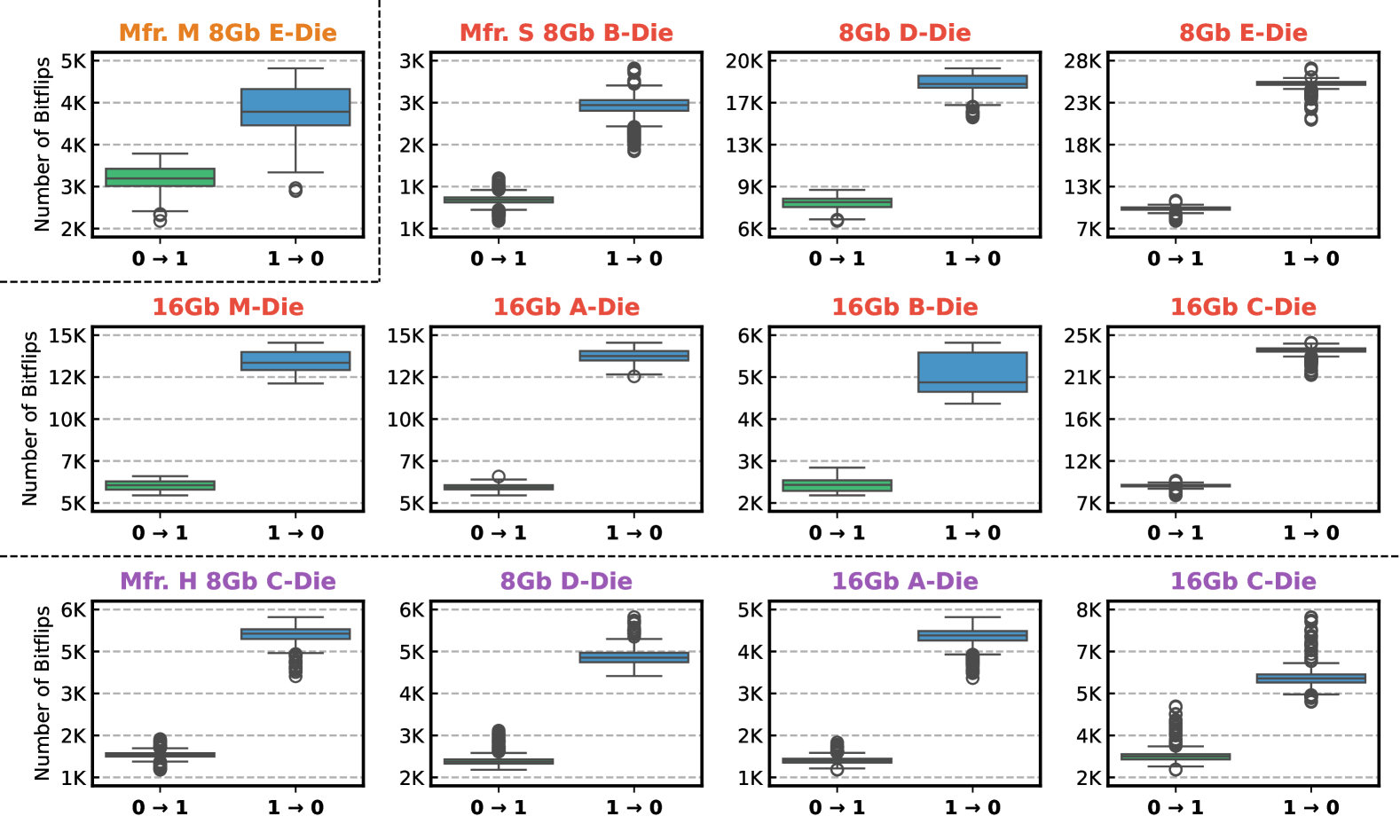
| Observation 3. Double-Sided RowHammer induces significantly more “1” to “0” bitflips than “0” to “1” bitflips at maximum aggressor row activation count. |
We observe that, for all the DRAM chips we test, Double-Sided RowHammer induces significantly more “1” to “0” than “0” to “1” bitflips at maximum aggressor row activation count. On average, the number of “1” to “0” bitflips in a victim row is higher than the number of “0” to “1” bitflips. This means that when the aggressor rows are hammered for sufficiently high number of times, more DRAM cells are vulnerable to “1” to “0” bitflips than “0” to “1” bitflips. Table 3 lists the average bitflip count (across all victim rows) of both “1” to “0” than “0” to “1” bitflips for all the DRAM chips we test.
| Mfr. | Die Density | Die Revision |
|
Difference |
|
|||||
|---|---|---|---|---|---|---|---|---|---|---|
| 0 to 1 | 1 to 0 | |||||||||
| S | 8Gb | B | 1769 | 3162 | 78.7% | 105.1% | ||||
| S | 8Gb | D | 8617 | 18803 | 118.2% | |||||
| S | 8Gb | E | 10414 | 25722 | 147.0% | |||||
| S | 16Gb | M | 6235 | 13631 | 118.6% | |||||
| S | 16Gb | A | 6070 | 13833 | 127.9% | |||||
| S | 16Gb | B | 2496 | 5564 | 122.8% | |||||
| S | 16Gb | C | 9621 | 23849 | 147.9% | |||||
| H | 8Gb | C | 2461 | 5417 | 120.1% | |||||
| H | 8Gb | D | 2619 | 5226 | 99.5% | |||||
| H | 16Gb | A | 2295 | 4807 | 109.4% | |||||
| H | 16Gb | C | 3586 | 6320 | 76.2% | |||||
| M | 8Gb | E | 3555 | 4593 | 29.2% | |||||
We derive the following key takeaway.
| Takeaway 3. For Double-Sided RowHammer, significantly more DRAM cells are vulnerable to the error mechanism for “1” to “0” bitflips than “0” to “1” bitflips, when the aggressor rows are hammered enough times. |
To further study the relationship between the number of “1” to “0” and “0” to “1” bitflips for double-sided RowHammer, we identify exactly when the number of “1” to “0” bitflips start to Exceeds the number of “0” to “1” bitflips. To do so, we gradually increase the aggressor row activation count (with a step size of 1000) from the HCFirst of “0” to “1” bitflips (denoted as HCFirst01) until we observe more “1” to “0” bitflips than “0” to “1” bitflips. We define the aggressor row activation count at this point as HC10Exceeds01. Table 4 compares the average HC10Exceeds01 to the average HCFirst01 for all DRAM chips we test. We observe that, on average, HC10Exceeds01 is higher than HCFirst01.
| Mfr. | Die Density | Die Revision | Aggr. Row Act. Count | Difference |
|
|||
|---|---|---|---|---|---|---|---|---|
| HCFirst01 | HC10Exceeds01 | |||||||
| S | 8 Gb | B | 43840 | 241740 | 451.4% | 406.5% | ||
| S | 8 Gb | D | 15398 | 63198 | 310.4% | |||
| S | 8 Gb | E | 9684 | 31927 | 229.7% | |||
| S | 16 Gb | M | 16732 | 72188 | 331.4% | |||
| S | 16 Gb | A | 16981 | 78820 | 364.2% | |||
| S | 16 Gb | B | 26415 | 153826 | 482.3% | |||
| S | 16 Gb | C | 11355 | 36751 | 223.6% | |||
| H | 8 Gb | C | 26500 | 156087 | 489.0% | |||
| H | 8 Gb | D | 22069 | 141656 | 541.9% | |||
| H | 16 Gb | A | 29825 | 175674 | 489.0% | |||
| H | 16 Gb | C | 18042 | 154951 | 758.8% | |||
| M | 8 Gb | E | 44468 | 235454 | 429.5% | |||
5.3 Bitflip Count with Single-Sided RowPress
Metric. To align the experimental characterization results with Characteristic 2, we test the maximum number of bitflips that can be induced within the refresh window (i.e., 64ms) for single-sided RowPress for both “0” to “1” and “1” to “0” bitflips.
Methodology. To cover both the NWL aggressor case and PWL aggressor case (Section 3.2), for each victim row, we perform single-sided RowPress on both its upper (i.e., victim row address + 1) aggressor row and lower (i.e., victim row address - 1) aggressor row. We keep the aggressor row open for as 1) it is a valid row open time upperbound indicated by the JEDEC DDR4 standard [94], and 2) it is long enough for the RowPress effect to dominate the RowHammer effect [6]. To induce as many RowPress bitflips as possible, we 1) activate the aggressor row as many times as possible within the 64ms refresh window [94] (7500 times), and 2) maintain DRAM temperature at 80∘C since prior works show that DRAM is much more vulnerable to single-sided RowPress at higher temperatures [6, 77, 79]. We initialize the victim row with either all-zeros (0x00) or all-ones (0xFF), and initialize the aggressor row with the opposite data of the victim row.
Results. Figure 5 plots the distribution of the total number of bitflips values per victim row (y-axis) with both “0” to “1” (i.e., the victim row has data 0x00) and “1” to “0” (i.e., the victim row has data 0xFF) bitflips (x-axis) for all DRAM chips we test in a box and whiskers plot. Blue represents the upper aggressor row case, and red represents the lower aggressor row case. We make the following observation from the results.
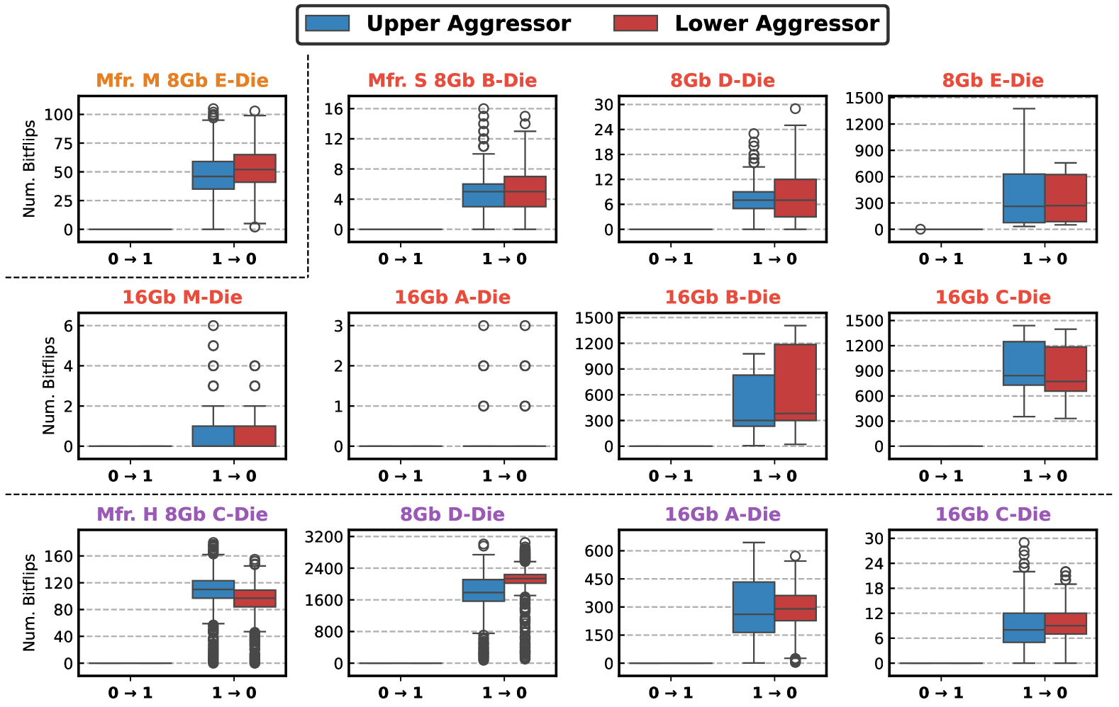
| Observation 4. Single-sided RowPress overwhelmingly induces “1” to “0” bitflips. |
We observe that for almost all the DRAM chips we test, Single-Sided RowPress induces only “1” to “0” bitflips but not “0” to “1” bitflips. The only exception is Mfr. S 8Gb E-Die where only one victim row has only one “0” to “1” bitflip. We do not observe a significant difference between the upper aggressor row case and the lower aggressor row case: on average across all DRAM chips we test, the number of bitflips that the upper aggressor induces is only smaller than that of the lower aggressor row.
| Takeaway 4. For Single-Sided RowPress, the observed error mechanism of “1” to “0” bitflips is much stronger than that of “0” to “1” bitflips. |
6 Inconsistencies and Implications
In this section, we first summarize the key inconsistencies between our experimental characterization results and the device-level read disturbance error mechanism prior works study. Second, we discuss the implications of our findings and propose hypotheses to explain the inconsistencies.
6.1 Inconsistencies Between Experimental Characterization and Device-Level Studies
Inconsistency 1. State-of-the-art device-level error mechanism to explain double-sided RowHammer [76] shows that double-sided RowHammer induces only “1” to “0” bitflips (Characteristic 1). However, our experimental characterization results with real DRAM chips show that double-sided RowHammer induces both “1” to “0” and “0” to “1” bitflips.
Inconsistency 2. State-of-the-art device-level error mechanism to explain double-sided RowHammer [76] demonstrates that the consecutive activation of NWL and PWL significantly enhances electron migration into the victim DRAM cell, thus enhancing “1” to “0” bitflips and mitigating “0” to “1” bitflips (Characteristic 1). However, our experimental characterization results show that double-sided RowHammer induces the initial “0” to “1” bitflips easier (i.e., requiring fewer aggressor row activations) than the initial “1” to “0” bitflips. This implies that the error mechanism for “0” to “1” bitflips is stronger than “1” to “0” bitflips in the most vulnerable cells (i.e., those requiring the least number of aggressor row activations to induce bitflips) .
Inconsistency 3. State-of-the-art device-level error mechanism to explain single-sided RowPress [77, 79] shows that RowPress should induce both “1” to “0” and “0” to “1” bitflips. However, our experimental characterization results show that even with a long aggressor row open time (i.e., ), a high aggressor row activation count (i.e., 7500), and using both the NWL and the PWL as the aggressor rows, the overwhelming majority of single-sided RowPress bitflips (except for only one) are “1” to “0” bitflips.
6.2 Potential Explanations for the Inconsistencies
The inconsistencies we identify implies that either 1) existing research on the device-level error mechanisms of DRAM read disturbance are not comprehensive enough to cover all the major leakage mechanisms, or 2) the state-of-the-art true- and anti-cell reverse engineering technique based on DRAM cell retention failures is incorrect.
Investigating the exact causes of the inconsistencies is outside the scope of this work. However, we still hypothesize several potential reasons that may cause the inconsistencies. First, existing device-level works often make assumptions and simplications when performing device-level simulations. For example, prior works that study the trap-assisted electron migration leakage mechanism only focus on a single acceptor-like trap [74, 76, 77, 79], without taking a deeper look into donor-like traps and potential dynamics among multiple trap locations.
Second, device-level simulations usually only model very few isolated structures and components (e.g., an active region, two NWLs and two PWLs). This modeling methodology potentially 1) misses key interactions and coupling between multiple devices, and 2) manufacturing variations that could become first-order effects when observed from real-chip experiments. For example, a study that models a whole DRAM row with a statistical modeling of the cell’s vulnerability distribution could help with understanding and explaining why Double-Sided RowHammer 1) first induces “0” to “1” bitflips with lower aggressor row activation counts compared to “1” to “0” bitflips (Takeaway 2), but 2) induces significantly more “1” to “0” bitflips than “0” to “1” bitflips when the aggressor rows are activated sufficiently large number of times (Takeaway 3).
Third, the observed bitflips from real-chip experiments are not only affected by the victim cell storage node voltage itself, but also other circuit components and mechanisms like bitline-bitline coupling noise [95, 96, 80], bitline sense amplifier (BLSA) offset voltage [96, 97, 88, 98], etc. For example, if the BLSA design and/or operation causes a significant asymmetry of the signal margin in sensing “1”s and “0”s, the real-chip experimental results will be heavily skewed towards one bitflip direction.
We hope that our results in this paper provide future works with insights into building a more fundamental and comprehensive understanding of DRAM read disturbance.
7 Related Work
To our knowledge, this is the first paper to systematically demonstrate the fundamental inconsistencies of DRAM read disturbance bitflip characteristics between real-chip experimental characterization and proposed device-level error mechanisms. Prior works on experimental characterization [2, 3, 4, 5, 6, 7, 12, 14, 15] do not involve alignment with device-level studies. Prior device-level studies [74, 75, 76, 77, 79] do not conduct experimental characterization using real DRAM chips that matches the conditions set in their simulations. Earlier work [99, 73] that conducts both real-chip characterizations and device-level simulations do not study the double-sided RowHammer and RowPress access patterns.
8 Conclusion
In this paper, we attempt to align and cross-validate the real-chip experimental characterization results and state-of-the-art device-level studies of DRAM read disturbance. Through our experiments, we identify fundamental inconsistencies in the RowHammer and RowPress bitflip directions and access pattern dependence between experimental characterization results and the device-level error mechanisms.
Based on our results, we hypothesize that either 1) existing research on the device-level error mechanisms of DRAM read disturbance are not comprehensive enough to cover all the major leakage mechanisms, or 2) the state-of-the-art true- and anti-cell reverse engineering technique based on DRAM cell retention failures is incorrect. We hope our findings inspire and enable future works to build a more fundamental and comprehensive understanding of DRAM read disturbance.
Acknowledgments
We thank the anonymous reviewers of VTS 2025 for feedback. We thank the SAFARI Research Group members for constructive feedback and the stimulating intellectual environment. We acknowledge the generous gift funding provided by our industrial partners (especially Google, Huawei, Intel, Microsoft), which has been instrumental in enabling the research we have been conducting on read disturbance in DRAM in particular and memory systems in general [13, 100]. This work was in part supported by a Google Security and Privacy Research Award and the Microsoft Swiss Joint Research Center.
References
- [1] Robert H. Dennard. Field-Effect Transistor Memory, 1968. U.S. Patent 3,387,286.
- [2] Y. Kim, R. Daly, J. Kim, C. Fallin, J. H. Lee, D. Lee, C. Wilkerson, K. Lai, and O. Mutlu. Flipping Bits in Memory Without Accessing Them: An Experimental Study of DRAM Disturbance Errors. In ISCA, 2014.
- [3] Jeremie S. Kim, Minesh Patel, Abdullah Giray Yağlıkçı, Hasan Hassan, Roknoddin Azizi, Lois Orosa, and Onur Mutlu. Revisiting RowHammer: An Experimental Analysis of Modern Devices and Mitigation Techniques. In ISCA, 2020.
- [4] Lois Orosa, A Giray Yağlıkçı, Haocong Luo, Ataberk Olgun, Jisung Park, Hasan Hassan, Minesh Patel, Jeremie S. Kim, and Onur Mutlu. A Deeper Look into RowHammer’s Sensitivities: Experimental Analysis of Real DRAM Chips and Implications on Future Attacks and Defenses. In MICRO, 2021.
- [5] A Giray Yağlıkçı, Haocong Luo, Geraldo Francisco Oliveira, Ataberk Olgun, Minesh Patel, Jisung Park, Hasan Hassan, Jeremie S. Kim, Lois Orosa, and Onur Mutlu. Understanding RowHammer Under Reduced Wordline Voltage: An Experimental Study Using Real DRAM Devices. In DSN, 2022.
- [6] Haocong Luo, Ataberk Olgun, Abdullah Giray Yağlıkçı, Yahya Can Tuğrul, Steve Rhyner, Meryem Banu Cavlak, Joël Lindegger, Mohammad Sadrosadati, and Onur Mutlu. RowPress: Amplifying Read Disturbance in Modern DRAM Chips. In ISCA, 2023.
- [7] Hwayong Nam, Seungmin Baek, Minbok Wi, Michael Jaemin Kim, Jaehyun Park, Chihun Song, Nam Sung Kim, and Jung Ho Ahn. DRAMScope: Uncovering DRAM Microarchitecture and Characteristics by Issuing Memory Commands . In ISCA, 2024.
- [8] Onur Mutlu. The RowHammer Problem and Other Issues We May Face as Memory Becomes Denser. In DATE, 2017.
- [9] Onur Mutlu and Jeremie S Kim. RowHammer: A Retrospective. TCAD, 2019.
- [10] Onur Mutlu, Ataberk Olgun, and A. Giray Yağlıkçı. Fundamentally Understanding and Solving RowHammer. In ASP-DAC, 2023.
- [11] Haocong Luo, Ataberk Olgun, Abdullah Giray Yağlıkçı, Yahya Can Tuğrul, Steve Rhyner, Meryem Banu Cavlak, Joël Lindegger, Mohammad Sadrosadati, and Onur Mutlu. RowPress Vulnerability in Modern DRAM Chips. In IEEE Micro, 2024.
- [12] Haocong Luo, Ismail Emir Yuksel, Ataberk Olgun, A. Giray Yaglikci, Mohammad Sadrosadati, and Onur Mutlu. An Experimental Characterization of Combined RowHammer and RowPress Read Disturbance in Modern DRAM Chips . In DSN Disrupt, 2024.
- [13] Onur Mutlu. Retrospective: Flipping Bits in Memory Without Accessing Them: An Experimental Study of DRAM Disturbance Errors. arXiv:2306.16093 [cs.CR], 2023.
- [14] Ataberk Olgun, Majd Osseiran, Abdullah Giray Yaglikci, Yahya Can Tugrul, Haocong Luo, Steve Rhyner, Behzad Salami, Juan Gomez Luna, and Onur Mutlu. Read Disturbance in High Bandwidth Memory: A Detailed Experimental Study on HBM2 DRAM Chips. In DSN, 2024.
- [15] Ataberk Olgun, Nisa Bostanci, Ismail Emir Yuksel, Abdullah Giray Yaglikci, Geraldo Francisco Oliveira, Haocong Luo, Oguzhan Canpolat, Minesh Patel, and Onur Mutlu. Variable Read Disturbance: An Experimental Analysis of Temporal Variation in DRAM Read Disturbance. In HPCA, 2025.
- [16] Daniel Gruss, Clementine Maurice, and Stefan Mangard. Rowhammer.js: A Remote Software-Induced Fault Attack in JavaScript. In DIMVA, 2016.
- [17] Apostolos P Fournaris, Lidia Pocero Fraile, and Odysseas Koufopavlou. Exploiting Hardware Vulnerabilities to Attack Embedded System Devices: A Survey of Potent Microarchitectural Attacks. Electronics, 2017.
- [18] Damian Poddebniak, Juraj Somorovsky, Sebastian Schinzel, Manfred Lochter, and Paul Rösler. Attacking Deterministic Signature Schemes using Fault Attacks. In EuroS&P, 2018.
- [19] Andrei Tatar, Radhesh Krishnan Konoth, Elias Athanasopoulos, Cristiano Giuffrida, Herbert Bos, and Kaveh Razavi. Throwhammer: Rowhammer Attacks Over the Network and Defenses. In USENIX ATC, 2018.
- [20] Sebastien Carre, Matthieu Desjardins, Adrien Facon, and Sylvain Guilley. OpenSSL Bellcore’s Protection Helps Fault Attack. In DSD, 2018.
- [21] Alessandro Barenghi, Luca Breveglieri, Niccolò Izzo, and Gerardo Pelosi. Software-Only Reverse Engineering of Physical DRAM Mappings for Rowhammer Attacks. In IVSW, 2018.
- [22] Zhenkai Zhang, Zihao Zhan, Daniel Balasubramanian, Xenofon Koutsoukos, and Gabor Karsai. Triggering Rowhammer Hardware Faults on ARM: A Revisit. In ASHES, 2018.
- [23] Sarani Bhattacharya and Debdeep Mukhopadhyay. Advanced Fault Attacks in Software: Exploiting the Rowhammer Bug. Fault Tolerant Architectures for Cryptography and Hardware Security, 2018.
- [24] Mark Seaborn and Thomas Dullien. Exploiting the DRAM Rowhammer Bug to Gain Kernel Privileges. http://googleprojectzero.blogspot.com.tr/2015/03/exploiting-dram-rowhammer-bug-to-gain.html, 2015.
- [25] SAFARI Research Group. RowHammer — GitHub Repository. https://github.com/CMU-SAFARI/rowhammer, 2021.
- [26] Mark Seaborn and Thomas Dullien. Exploiting the DRAM Rowhammer Bug to Gain Kernel Privileges. Black Hat, 2015.
- [27] Victor van der Veen, Yanick Fratantonio, Martina Lindorfer, Daniel Gruss, Clementine Maurice, Giovanni Vigna, Herbert Bos, Kaveh Razavi, and Cristiano Giuffrida. Drammer: Deterministic Rowhammer Attacks on Mobile Platforms. In CCS, 2016.
- [28] Kaveh Razavi, Ben Gras, Erik Bosman, Bart Preneel, Cristiano Giuffrida, and Herbert Bos. Flip Feng Shui: Hammering a Needle in the Software Stack. In USENIX Security, 2016.
- [29] Peter Pessl, Daniel Gruss, Clémentine Maurice, Michael Schwarz, and Stefan Mangard. DRAMA: Exploiting DRAM Addressing for Cross-CPU Attacks. In USENIX Security, 2016.
- [30] Yuan Xiao, Xiaokuan Zhang, Yinqian Zhang, and Radu Teodorescu. One Bit Flips, One Cloud Flops: Cross-VM Row Hammer Attacks and Privilege Escalation. In USENIX Security, 2016.
- [31] Erik Bosman, Kaveh Razavi, Herbert Bos, and Cristiano Giuffrida. Dedup Est Machina: Memory Deduplication as an Advanced Exploitation Vector. In S&P, 2016.
- [32] Sarani Bhattacharya and Debdeep Mukhopadhyay. Curious Case of Rowhammer: Flipping Secret Exponent Bits Using Timing Analysis. In CHES, 2016.
- [33] Wayne Burleson, Onur Mutlu, and Mohit Tiwari. Invited: Who is the Major Threat to Tomorrow’s Security? You, the Hardware Designer. In DAC, 2016.
- [34] Rui Qiao and Mark Seaborn. A New Approach for RowHammer Attacks. In HOST, 2016.
- [35] Ferdinand Brasser, Lucas Davi, David Gens, Christopher Liebchen, and Ahmad-Reza Sadeghi. Can’t Touch This: Software-Only Mitigation Against Rowhammer Attacks Targeting Kernel Memory. In USENIX Security, 2017.
- [36] Yeongjin Jang, Jaehyuk Lee, Sangho Lee, and Taesoo Kim. SGX-Bomb: Locking Down the Processor via Rowhammer Attack. In SOSP, 2017.
- [37] Misiker Tadesse Aga, Zelalem Birhanu Aweke, and Todd Austin. When Good Protections Go Bad: Exploiting Anti-DoS Measures to Accelerate Rowhammer Attacks. In HOST, 2017.
- [38] Andrei Tatar, Cristiano Giuffrida, Herbert Bos, and Kaveh Razavi. Defeating Software Mitigations Against Rowhammer: A Surgical Precision Hammer. In RAID, 2018.
- [39] Daniel Gruss, Moritz Lipp, Michael Schwarz, Daniel Genkin, Jonas Juffinger, Sioli O’Connell, Wolfgang Schoechl, and Yuval Yarom. Another Flip in the Wall of Rowhammer Defenses. In S&P, 2018.
- [40] Moritz Lipp, Misiker Tadesse Aga, Michael Schwarz, Daniel Gruss, Clémentine Maurice, Lukas Raab, and Lukas Lamster. Nethammer: Inducing Rowhammer Faults Through Network Requests. arXiv:1805.04956 [cs.CR], 2018.
- [41] Victor van der Veen, Martina Lindorfer, Yanick Fratantonio, Harikrishnan Padmanabha Pillai, Giovanni Vigna, Christopher Kruegel, Herbert Bos, and Kaveh Razavi. GuardION: Practical Mitigation of DMA-Based Rowhammer Attacks on ARM. In DIMVA, 2018.
- [42] Pietro Frigo, Cristiano Giuffrida, Herbert Bos, and Kaveh Razavi. Grand Pwning Unit: Accelerating Microarchitectural Attacks with the GPU. In S&P, 2018.
- [43] Lucian Cojocar, Kaveh Razavi, Cristiano Giuffrida, and Herbert Bos. Exploiting Correcting Codes: On the Effectiveness of ECC Memory Against Rowhammer Attacks. In S&P, 2019.
- [44] Sangwoo Ji, Youngjoo Ko, Saeyoung Oh, and Jong Kim. Pinpoint Rowhammer: Suppressing Unwanted Bit Flips on Rowhammer Attacks. In ASIACCS, 2019.
- [45] Sanghyun Hong, Pietro Frigo, Yiğitcan Kaya, Cristiano Giuffrida, and Tudor Dumitraş. Terminal Brain Damage: Exposing the Graceless Degradation in Deep Neural Networks Under Hardware Fault Attacks. In USENIX Security, 2019.
- [46] Andrew Kwong, Daniel Genkin, Daniel Gruss, and Yuval Yarom. RAMBleed: Reading Bits in Memory Without Accessing Them. In S&P, 2020.
- [47] Pietro Frigo, Emanuele Vannacci, Hasan Hassan, Victor van der Veen, Onur Mutlu, Cristiano Giuffrida, Herbert Bos, and Kaveh Razavi. TRRespass: Exploiting the Many Sides of Target Row Refresh. In S&P, 2020.
- [48] Lucian Cojocar, Jeremie Kim, Minesh Patel, Lillian Tsai, Stefan Saroiu, Alec Wolman, and Onur Mutlu. Are We Susceptible to Rowhammer? An End-to-End Methodology for Cloud Providers. In S&P, 2020.
- [49] Zane Weissman, Thore Tiemann, Daniel Moghimi, Evan Custodio, Thomas Eisenbarth, and Berk Sunar. JackHammer: Efficient Rowhammer on Heterogeneous FPGA–CPU Platforms. IACR Transactions on Cryptographic Hardware and Embedded Systems, 2020.
- [50] Zhi Zhang, Yueqiang Cheng, Dongxi Liu, Surya Nepal, Zhi Wang, and Yuval Yarom. PThammer: Cross-User-Kernel-Boundary Rowhammer through Implicit Accesses. In MICRO, 2020.
- [51] Fan Yao, Adnan Siraj Rakin, and Deliang Fan. DeepHammer: Depleting the Intelligence of Deep Neural Networks Through Targeted Chain of Bit Flips. In USENIX Security, 2020.
- [52] Finn de Ridder, Pietro Frigo, Emanuele Vannacci, Herbert Bos, Cristiano Giuffrida, and Kaveh Razavi. SMASH: Synchronized Many-Sided Rowhammer Attacks from JavaScript. In USENIX Security, 2021.
- [53] Hasan Hassan, Yahya Can Tugrul, Jeremie S. Kim, Victor van der Veen, Kaveh Razavi, and Onur Mutlu. Uncovering in-DRAM RowHammer Protection Mechanisms: A New Methodology, Custom RowHammer Patterns, and Implications. In MICRO, 2021.
- [54] Patrick Jattke, Victor van der Veen, Pietro Frigo, Stijn Gunter, and Kaveh Razavi. Blacksmith: Scalable Rowhammering in the Frequency Domain. In SP, 2022.
- [55] M Caner Tol, Saad Islam, Berk Sunar, and Ziming Zhang. Toward Realistic Backdoor Injection Attacks on DNNs using RowHammer. arXiv:2110.07683v2 [cs.LG], 2022.
- [56] Andreas Kogler, Jonas Juffinger, Salman Qazi, Yoongu Kim, Moritz Lipp, Nicolas Boichat, Eric Shiu, Mattias Nissler, and Daniel Gruss. Half-Double: Hammering From the Next Row Over. In USENIX Security, 2022.
- [57] Lois Orosa, Ulrich Rührmair, A Giray Yaglikci, Haocong Luo, Ataberk Olgun, Patrick Jattke, Minesh Patel, Jeremie Kim, Kaveh Razavi, and Onur Mutlu. SpyHammer: Using RowHammer to Remotely Spy on Temperature. arXiv:2210.04084, 2022.
- [58] Zhi Zhang, Wei He, Yueqiang Cheng, Wenhao Wang, Yansong Gao, Dongxi Liu, Kang Li, Surya Nepal, Anmin Fu, and Yi Zou. Implicit Hammer: Cross-Privilege-Boundary Rowhammer through Implicit Accesses. IEEE Transactions on Dependable and Secure Computing, 2022.
- [59] Liang Liu, Yanan Guo, Yueqiang Cheng, Youtao Zhang, and Jun Yang. Generating Robust DNN with Resistance to Bit-Flip based Adversarial Weight Attack. IEEE Transactions on Computers, 2022.
- [60] Yaakov Cohen, Kevin Sam Tharayil, Arie Haenel, Daniel Genkin, Angelos D Keromytis, Yossi Oren, and Yuval Yarom. HammerScope: Observing DRAM Power Consumption Using Rowhammer. In CCS, 2022.
- [61] Mengxin Zheng, Qian Lou, and Lei Jiang. TrojViT: Trojan Insertion in Vision Transformers. arXiv:2208.13049, 2022.
- [62] Michael Fahr Jr, Hunter Kippen, Andrew Kwong, Thinh Dang, Jacob Lichtinger, Dana Dachman-Soled, Daniel Genkin, Alexander Nelson, Ray Perlner, Arkady Yerukhimovich, et al. When Frodo Flips: End-to-End Key Recovery on FrodoKEM via Rowhammer. CCS, 2022.
- [63] Youssef Tobah, Andrew Kwong, Ingab Kang, Daniel Genkin, and Kang G. Shin. SpecHammer: Combining Spectre and Rowhammer for New Speculative Attacks. In SP, 2022.
- [64] Adnan Siraj Rakin, Md Hafizul Islam Chowdhuryy, Fan Yao, and Deliang Fan. DeepSteal: Advanced Model Extractions Leveraging Efficient Weight Stealing in Memories. In SP, 2022.
- [65] Jonas Juffinger, Sudheendra Raghav Neela, Martin Heckel, Lukas Schwarz, Florian Adamsky, and Daniel Gruss. Presshammer: Rowhammer and Rowpress Without Physical Address Information. In DIMVA, 2024.
- [66] Patrick Jattke, Max Wipfli, Flavien Solt, Michele Marazzi, Matej Bölcskei, and Kaveh Razavi. ZenHammer: Rowhammer Attacks on AMD Zen-based Platforms. In USENIX Security, 2024.
- [67] Finn de Ridder, Patrick Jattke, and Kaveh Razavi. Posthammer: Pervasive Browser-based Rowhammer Attacks with Postponed Refresh Commands. In USENIX Security, 2025.
- [68] Anandpreet Kaur, Pravin Srivastav, and Bibhas Ghoshal. Flipping Bits Like a Pro: Precise Rowhammering on Embedded Devices. IEEE Embedded Systems Letters, 2023.
- [69] M. Caner Tol, Saad Islam, Andrew J. Adiletta, Berk Sunar, and Ziming Zhang. Don’t Knock! Rowhammer at the Backdoor of DNN Models. In DSN, 2023.
- [70] Koksal Mus, Yarkın Doröz, M. Caner Tol, Kristi Rahman, and Berk Sunar. Jolt: Recovering TLS Signing Keys via Rowhammer Faults. In SP, 2023.
- [71] Dawei Li, Di Liu, Yangkun Ren, Ziyi Wang, Yu Sun, Zhenyu Guan, Qianhong Wu, and Jianwei Liu. FPHammer: A Device Identification Framework based on DRAM Fingerprinting. In TrustCom, 2023.
- [72] Seungmin Baek, Minbok Wi, Seonyong Park, Hwayong Nam, Michael Jaemin Kim, Nam Sung Kim, and Jung Ho Ahn. Marionette: A rowhammer attack via row coupling. In ASPLOS, 2025.
- [73] Seong-Wan Ryu, Kyungkyu Min, Jungho Shin, Heimi Kwon, Donghoon Nam, Taekyung Oh, Tae-Su Jang, Minsoo Yoo, Yongtaik Kim, and Sungjoo Hong. Overcoming the Reliability Limitation in the Ultimately Scaled DRAM using Silicon Migration Technique by Hydrogen Annealing. In IEDM, 2017.
- [74] Thomas Yang and Xi-Wei Lin. Trap-Assisted DRAM Row Hammer Effect. EDL, 2019.
- [75] Andrew J. Walker, Sungkwon Lee, and Dafna Beery. On DRAM RowHammer and the Physics on Insecurity. IEEE TED, 2021.
- [76] Longda Zhou, Jie Li, Zheng Qiao, Pengpeng Ren, Zixuan Sun, Jianping Wang, Blacksmith Wu, Zhigang Ji, Runsheng Wang, Kanyu Cao, and Ru Huang. Double-sided Row Hammer Effect in Sub-20 nm DRAM: Physical Mechanism, Key Features and Mitigation. In IRPS, 2023.
- [77] Longda Zhou, Sheng Ye, Runsheng Wang, and Zhigang Ji. Unveiling RowPress in Sub-20 nm DRAM Through Comparative Analysis With Row Hammer: From Leakage Mechanisms to Key Features. In IEEE Transactions on Electron Devices, 2024.
- [78] Jie Li, Longda Zhou, Sheng Ye, Zheng Qiao, and Zhigang Ji. Understanding the Competitive Interaction in Leakage Mechanisms for Effective Row Hammer Mitigation in Sub-20 nm DRAM. In IEEE Electron Device Letters, 2024.
- [79] Longda Zhou, Jie Li, Pengpeng Ren, Sheng Ye, Da Wang, Zheng Qiao, and Zhigang Ji. Understanding the Physical Mechanism of RowPress at the Device-Level in Sub-20 nm DRAM. In IRPS, 2024.
- [80] Jamie Liu, Ben Jaiyen, Yoongu Kim, Chris Wilkerson, Onur Mutlu, J Liu, B Jaiyen, Y Kim, C Wilkerson, and O Mutlu. An Experimental Study of Data Retention Behavior in Modern DRAM Devices. In ISCA, 2013.
- [81] Ataberk Olgun, Hasan Hassan, A. Giray Yaglikci, Yahya Can Tugrul, Lois Orosa, Haocong Luo, Minesh Patel, Oguz Ergin, and Onur Mutlu. DRAM Bender: An Extensible and Versatile FPGA-based Infrastructure to Easily Test State-of-the-art DRAM Chips. TCAD, 2023.
- [82] Hasan Hassan, Nandita Vijaykumar, Samira Khan, Saugata Ghose, Kevin Chang, Gennady Pekhimenko, Donghyuk Lee, Oguz Ergin, and Onur Mutlu. SoftMC: A Flexible and Practical Open-Source Infrastructure for Enabling Experimental DRAM Studies. In HPCA, 2017.
- [83] Minesh Patel, Jeremie S Kim, and Onur Mutlu. The Reach Profiler (REAPER): Enabling the Mitigation of DRAM Retention Failures via Profiling at Aggressive Conditions. In ISCA, 2017.
- [84] Samira Khan, Donghyuk Lee, Yoongu Kim, Alaa R Alameldeen, Chris Wilkerson, and Onur Mutlu. The Efficacy of Error Mitigation Techniques for DRAM Retention Failures: A Comparative Experimental Study. In SIGMETRICS, 2014.
- [85] Samira Khan, Donghyuk Lee, and Onur Mutlu. PARBOR: An Efficient System-Level Technique to Detect Data-Dependent Failures in DRAM. In DSN, 2016.
- [86] Minesh Patel, Jeremie Kim, Taha Shahroodi, Hasan Hassan, and Onur Mutlu. Bit-Exact ECC Recovery (BEER): Determining DRAM On-Die ECC Functions by Exploiting DRAM Data Retention Characteristics (Best Paper). In MICRO, 2020.
- [87] SAFARI Research Group. Revisiting DRAM Read Disturbance — GitHub Repository. https://github.com/CMU-SAFARI/ReadDisturbanceVTS25, 2025.
- [88] R. Kraus and K. Hoffmann. Optimized sensing scheme of DRAMs. IEEE Journal of Solid-State Circuits, 1989.
- [89] Brent Keeth, R Jacob Baker, Brian Johnson, and Feng Lin. DRAM Circuit Design: Fundamental and High-Speed Topics. John Wiley & Sons, 2007.
- [90] Seungki Hong, Dongha Kim, Jaehyung Lee, Reum Oh, Changsik Yoo, Sangjoon Hwang, and Jooyoung Lee. DSAC: Low-Cost RowHammer Mitigation Using In-DRAM Stochastic and Approximate Counting Algorithm. arXiv:2302.03591, 2023.
- [91] SAFARI Research Group. DRAM Bender — GitHub Repository. https://github.com/CMU-SAFARI/DRAM-Bender, 2022.
- [92] SAFARI Research Group. SoftMC — GitHub Repository. https://github.com/CMU-SAFARI/softmc, 2021.
- [93] Maxwell. FT20X. https://www.maxwell-fa.com/upload/files/base/8/m/311.pdf.
- [94] JEDEC. JESD79-4C: DDR4 SDRAM Standard, 2020.
- [95] Dong-Sun Min and D.W. Langer. Multiple twisted dataline techniques for multigigabit DRAMs. IEEE Journal of Solid-State Circuits, 1999.
- [96] Yan Li, Helmut Schneider, Florian Schnabel, Roland Thewes, and Doris Schmitt-Landsiedel. DRAM Yield Analysis and Optimization by a Statistical Design Approach. IEEE Transactions on Circuits and Systems I: Regular Papers, 2011.
- [97] D.G. Laurent. Sense Amplifier Signal Margins and Process Sensitivities. IEEE Transactions on Circuits and Systems I: Fundamental Theory and Applications, 2002.
- [98] Myoung Jin Lee, Ki Myung Kyung, Hyung Sik Won, Myoung Su Lee, and Kun Woo Park. A Bitline Sense Amplifier for Offset Compensation. In ISSCC, 2010.
- [99] Kyungbae Park, Chulseung Lim, Donghyuk Yun, and Sanghyeon Baeg. Experiments and Root Cause Analysis for Active-Precharge Hammering Fault in DDR3 SDRAM under 3xnm Technology. Microelectronics Reliability, 2016.
- [100] Onur Mutlu, Saugata Ghose, Juan Gomez-Luna, Rachata Ausavarungnirun, Mohammad Sadrosadati, and Geraldo F. Oliveira. A Modern Primer on Processing in Memory. In arXiv. 2025.