Surface phonons in MoS2
Abstract
The thermal and electronic performance of atomically thin semiconductors is underpinned by their vibrational dynamics, yet surface phonons in layered materials remain poorly understood due to limitations in conventional experimental techniques. We employ helium-3 spin-echo (HeSE) spectroscopy to resolve the lowest energy () dispersions of surface phonons on bulk molybdenum disulfide (MoS2) with sub-meV energy resolution near . We identify two low-energy optical modes, and , exhibiting unexpected quasi-acoustic dispersion, and crucially do not find evidence of an acoustic mode at the surface. follows a purely quadratic dispersion (), while displays quartic behaviour (), indicative of strong anharmonicity. These modes, absent in inelastic x-ray scattering (IXS) measurements and theoretical predictions of the bulk, exhibit finite-layer confinement equivalent to 4.5 and 6 layers, respectively. Their rapid dispersion yields substantial group velocities at small wavevectors, suggesting a dominant role in surface and few-layer thermal transport. This work establishes optical surface phonons as key drivers of thermal management in 2D materials and highlights the necessity of understanding surface phononics for designing next-generation optoelectronic devices.
keywords:
molybdenum disulfide, surface phonon, 3He spin-echoCambridge] Cavendish Laboratory, Department of Physics, University of Cambridge, JJ Thomson Ave, Cambridge, UK \abbreviationsHeSE, MoS2, TMD
1 Introduction
Two-dimensional layered materials, such as transition metal dichalcogenides (TMDs), have been widely implemented into optoelectronic devices because of a range of tunable optical and electronic properties, via parameters such as thickness1, 2, 3, defect density4, passivation5 or surface functionalization6. Understanding the thermal properties of these materials is crucial to their successful integration into devices. The lowest energy, most fundamental, vibrational modes that are invariably present at device operating temperatures underpin the thermal, and by extension electronic, performance of the material, and therefore device performance as a whole. The characterisation of low energy modes is itself more challenging than for higher energy modes, but the dimensionality of TMDs means the cross-section for the phonon-probe interaction is significantly reduced compared to bulk samples as most techniques are not specifically surface sensitive.
Typical low energy phonon characterisation techniques include Raman 7, 8 and electron energy loss spectroscopy (EELS) 9. Low energy Raman is widely used for its accessibility and ability to measure modes but is limited to Raman active vibrational modes which, by definition, lie on the high symmetry point and is not specifically surface sensitive. Alternatively, one can use EELS, whose surface sensitivity is dependent on incident electron energy that can penetrate a material by a few atomic layers, to measure full dispersion curves. Cutting-edge EELS instruments, however, have a lower limit on accessible phonon modes that prevent measurement of the absolute lowest energy surface modes. In the current work we use 3He spin-echo (HeSE)10, 11, an atom spectroscopy technique with absolute surface sensitivity capable of measuring excitations in the few meV range, to measure the dispersion of the lowest energy surface phonons along the -K azimuth of MoS2, a prototypical layered semiconductor in the TMD family. We use a low energy () 3He beam such that, in a classical approximation, its reversal point is above the ionic cores of the surface atoms, scattering only from the outermost electron density12. HeSE can be seen as the surface sensitive counterpart to bulk measurements from inelastic neutron scattering13. We measure the ultra low energy, , dispersion of the and modes from the surface of MoS2. Our HeSE measurements of the surface modes show significant deviation from existing measurements of bulk MoS2 using inelastic x-ray scattering (IXS). Our results reveal the presence of finite depth surface modes by comparison to Raman studies of true few-layer MoS2. Although optical, these modes’ dispersions are strongly non-linear and unlike previous experimental and theoretical reports. Additionally, we find no acoustic modes at the surface of MoS2 and rather determine that the lowest energy optical modes have quasi-acoustic character, gaining significant group velocity at low wavevectors such that they contribute significantly to thermal transport at the surface.
2 3He spin-echo (HeSE) spectrometer
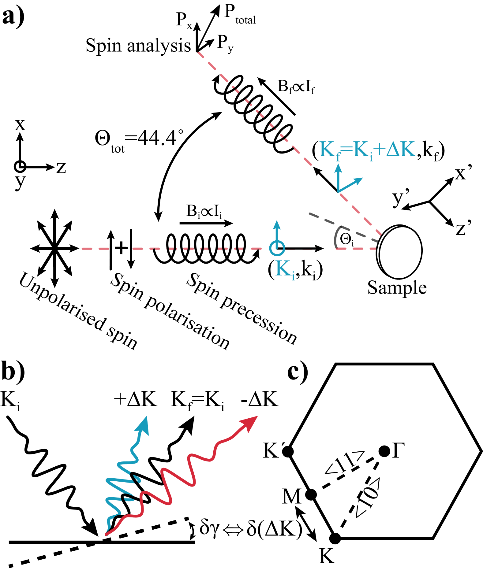
The 3He Spin Echo Spectrometer (HeSE) is a scattering technique that uses the encoded nuclear spins of helium atoms to measure inelastic processes at surfaces. A schematic of HeSE is shown in figure 1: a jet of 3He atoms is created from an expansion of high pressure gas into vacuum, with the centreline selected to form an approximately monochromatic beam14. The beam is spin polarized perpendicular to the propagation direction using a magnetic hexapole15, the polarized beam passes through a first uniform magnetic field, oriented (anti-)parallel to the beam axis, causing the spin undergo Larmor precession, encoding a phase to the spin states, prior to scattering from the sample. The spin encoded atom beam scatters from the sample with a total scattering angle of . The scattered beam passes through a second uniform magnetic field, causing further precession of the spin, . Finally, a second magnetic hexapole allows the measurement of the final spin state of the 3He atoms. The final polarization (expressed as a complex number ) has been shown10, 16 to be a Fourier transform of the ‘wavelength-intensity-matrix’
| (1) |
where is the relative intensity of incoming and outgoing de Broglie wavelengths of the 3He atoms. An inverse transformation allows the recovery of from the measured polarization, . A simple transformation from de Broglie wavelength to energy, , recovers an energy loss/gain spectrum, for the helium-surface scattering event. The so called ‘tilted projection measurement’ allows a full recovery of without measuring the full 2D space using a fixed ratio of , for further details see Alexandrowicz et al.10. An example polarization measurement is shown in figure 2 (a) and the energy spectrum recovered via appropriate transforms is shown in 2 (b). For further details of surface excitation measurements with HeSE consult Alexandrowicz et al.10 and Kole et al.16.
The low energies of the probe helium atoms, , means that scattering occurs exclusively from the top layer of atoms in a surface12. If there are surface excitations of the appropriate energies, creation or annihilation processes can occur via momentum transfer to or from the beam, resulting in peaks in the energy spectrum at or , respectively. Any particular spectrum, such as that in figure 2 (b), is recovered with a fixed scattering geometry set by the angle of the crystal relative to the incident and scattered beams, as shown in figure 1 (b). By changing the tilt angle of the crystal, canonically termed , and taking into account any change in energy of the helium atoms, the momentum exchange parallel to the surface, labelled , can be varied. A series of inelastic HeSE scans can then be used to build up a map of inelastic features as a function of , recovering the dispersion curve for the identified inelastic features.
3 Results
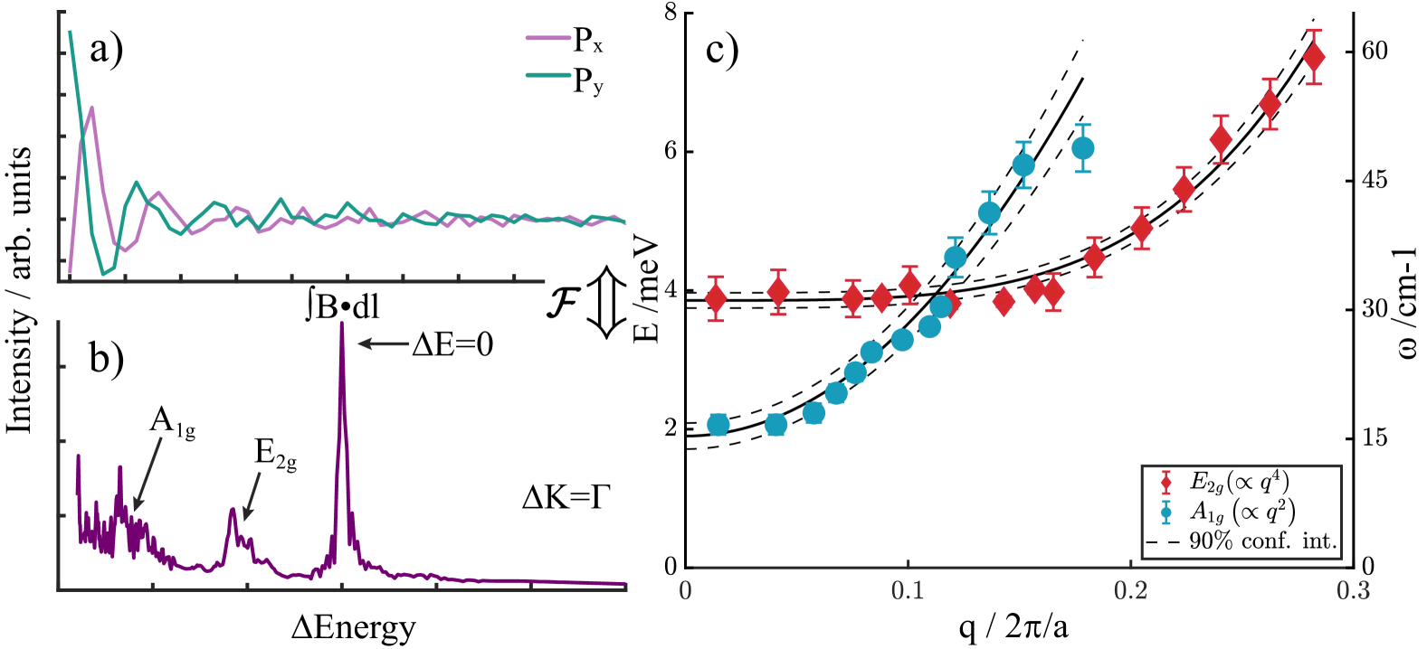
Figure 2 (c) presents the measured dispersion curve using HeSE along the K direction of the MoS2 lattice for 2 vibrational modes that we identify as the and optical modes at by comparison to low energy Raman spectroscopy and theoretical calculations17, 8. Moving from we find that the phonon branches cross each other at . First inspecting (out-of-plane compression mode), we find that its dispersion is well described by a pure quadratic function (). From the pure quadratic fit, we can extrapolate the energy of at (leftmost measured value at ) to determine the mode’s energy as . The dispersion of strongly agrees with purely quartic dispersion (), indicating a high degree of anharmonicity and displays near-dispersion-less character for . Due to the high resolution of the HeSE measurements in both energy and there is limited literature to compare to when .
Inelasitc X-=ray scattering (IXS) provides the most comprehensive experimental datasets availble for the low energy phonon modes in bulk MoS2. We compare to Tornatzky et al.18, plotted along with our HeSE data in figure 3, due to their recency, resolution, and comprehensive dataset which is also evaluated against their own calculations. Some literature measurements on bulk MoS2 exist using inelastic neutron scattering19 and high-resolution electron-energy-loss spectroscopy (HREELS)9, but these data lack resolution in both energy and momentum for quantitative comparison.
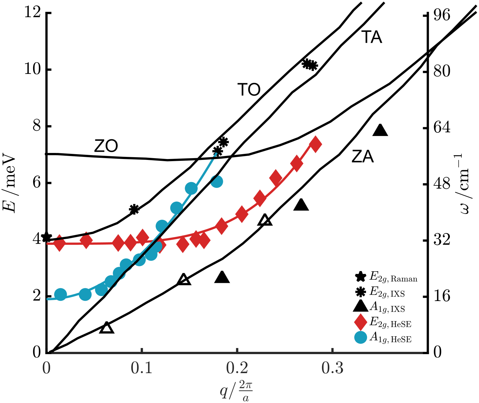
Tornatzky et al. measure two phonon branches with approximately linear dispersion at , that are attributed to two phonon branches - transverse in-plane optical (TO, ) and out-of-plane acoustic (ZA, ) modes in the lowest energy case by comparison to their own calculated dispersions. The modes’ dispersions, calculated by Tornatzky et al.18, in bulk MoS2 show strong agreement with IXS and Raman (black star, Zeng et al.17) measurements, validating that the behaviour of these modes is well captured by current theoretical understanding.
HeSE measurements, however, differ significantly from current measurements and theory on bulk MoS2. One immediately notices that HeSE does not observe any acoustic mode at the surface. With the knowledge that 17, 20, where is the number of layers, we suggest that the out-of-plane acoustic (ZA) mode predicted by DFT hardens significantly near , becoming an out-of-plane optical (ZO) mode at the material’s surface, with overall behaviour that is a hybrid of TA and ZO bulk predictions. From this layer-dependent relation, we also find that agrees with Raman measurements of a 6 layer thick MoS2 system at , quantifying the mode’s degree of surface confinement. The mode’s dispersion also changes significantly, in the bulk it has clear linear character for small wavevectors whereas at the surface we find strong agreement with purely quadratic dispersion, as shown in figure 2. The higher-order dispersion indicates that, although optical, the mode likely contributes significantly to thermal transport due to its rapidly increasing group velocity at the surface of the bulk and in the few-layer regime.
Inspecting the measurements at in figure 3, we observe a slight softening of the mode with respect to literature measurements with Raman (black star17) and infrared spectroscopies (black sqaure17), and the calculated value of TO. The three literature values show strong agreement with eachother, all lying within . The softening of the mode is known to correspond to the number of sample layers by the linear-chain model presented by Tan et al.21. Using the linear-chain model we report that the surface mode measured by HeSE corresponds to a 4-5 layer system, allowing for uncertainty, quantifying the mode’s degree of surface confinement. The dispersion of the HeSE measurements differs significantly, however, from the strongly agreeing IXS and DFT values. We report that this mode is significantly less dispersive than its bulk counterpart, being nearly flat for , but rapidly disperses thereafter, strongly agreeing with a purely quartic character, as shown in figure 2. Thus we suggest that the mode also contributes significantly to thermal transport at the surface of the bulk, and in the few-layer regime.
Having assigned our surface modes to their bulk equivalents as ZO (blue line) and TO (red line) we therefore assign the crossing at to the crossing between TO and ZO that Tornatzky et al. calculate at for bulk MoS2.
We note that HeSE measurements in figure 3 do not report any data that could be attributed to any part of the calculated ZA and TA bulk dispersion curves, of which the ZA mode has also been measured at small wavevectors by IXS. It is critical to note that because the 3He probe does not interact via polarisation of the material, HeSE is not subject to optical selection rules and will therefore, in principle, detect any vibration present, whether acoustic or optical, much akin to its counterpart bulk technique inelastic neutron scattering. With an upper limit on detectable energy of we are confident that there is no truly acoustic mode at the surface of MoS2 and that the calculated bulk ZO is also not present.
One typically finds that the vibrational modes found at the surface have similar dispersive character to their bulk counterparts but experience hardening or softening throughout momentum transfer space, holding for all crystal structures measured with HAS that have strong covalent, ionic or metallic bonding in all directions22. The absolute surface sensitivity of helium atom scattering therefore usually reveals surface-localised bulk modes rather than ones with entirely distinct energetic and dispersive character as we observe here.
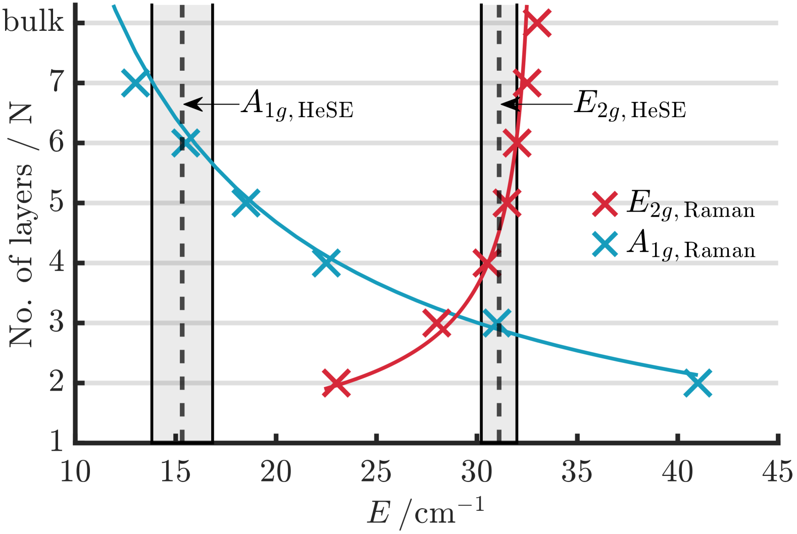
The energies of the and modes as a function of number of sample layers has previously been studied using Raman spectroscopy by Zeng et al.17. Zeng et al. measured MoS2 flakes of 1-7 layer, and bulk, thickness as shown in figure 4 where we reproduce their data. In figure 4 the (red crosses) and (blue crosses) modes’ energies are plotted as a function of sample thickness. One can use both the absolute energies of the two modes, and their as a fine measure of sample layer thickness due to them each having strong, but opposite, hardening/softening as a function of sample thickness. The presence of in the HeSE data further supports that the helium beam experiences the surface of the bulk MoS2 as a system with finite thickness due to the aforementioned relationship, fitted to data in figure 4 as a solid blue line. Inspecting figure 4 and comparing to the HeSE value strongly agrees with a 6-layer system. shows less precise agreement, ranging from 4-6 layers when allowing for uncertainty bounds. has significantly weaker proportionality of its energy with compared to , placing adjacent data apart in the -layer region. The linear-chain model21, , where , , , and represent the frequency of (), speed of light (), interlayer force constant per unit area and the number of sample layers, respectively, fully captures the behaviour of as a function of sample thickness, fitted curve shown in figure 4 as a solid red line.
Although there is a wealth of calculations of phonon dispersion in bulk and monolayer MoS2, there is little literature on few-layer systems. From figure 4 we have found that the energies of our modes agree with both calculated and experimental (Raman spectroscopy), indicating truly few-layer vibrational behaviour, or surface confinement, of 4-5 and 6 layers for and , respectively. While full calculations on finite layer MoS2 are not currently available in the literature a stidy of monolayer, 5-layer and bulk WS2 has been performed by K. Wilczynski, A.P. Gertych, K. Czerniak-Łosiewicz et al.23. Although the metal atoms are different, the structure remains highly similar, thus one expects the overall relation of phonon dispersion to layer-dependence to be qualitatively comparable. The authors report splitting of the lowest energy optical branches into 12 distinct modes at alongside the 3 acoustic modes similar to those present in the bulk material. At we only observe two optical modes and no evidence of acoustic modes.
4 Discussion
The HeSE measurements presented reveal the unique surface phonon dynamics of MoS2, offering critical insights into the vibrational behaviour of van Der Waals-bound layered materials. Our results demonstrate that the surface of bulk MoS2 hosts two low-energy optical phonon modes, and , with distinct dispersion characteristics. The mode exhibits purely quadratic dispersion (), while the mode follows a quartic relation (), indicative of significant anharmonic contributions. These dispersion characteristics deviate markedly from bulk measurements and calculations (IXS and DFT, respectively), which report approximately linear dispersion for analogous bulk modes. The observed non-linear behaviour suggests that these surface-localized modes acquire quasi-acoustic character, enabling substantial group velocities () even at small wavevectors. The quasi-acoustic nature implies that these modes contribute meaningfully to thermal transport at the surface, as thermal conductivity () scales with .
A key finding is the absence of truly acoustic modes, such as the Rayleigh wave, which are typically observed in non-layered 3D crystals using surface-sensitive techniques like HeSE and HAS. Their absence highlights the distinct vibrational landscape of layered materials, where surface phonons are influenced by finite-depth confinement due to comparatively weak inter-layer binding. By comparing the measured mode energies to Raman studies of few-layer MoS2 in figure 4, we attribute the surface dynamics to vibrational behaviour akin to 4.5 and 6.3 layer systems for and respectively. The energy ( at ) aligns with Raman data for 6-layer systems, while the mode corresponds to 4.5 layers. The finite-layer character quantifies the surface confinement depth, alternatively termed as coherence lengths of () and ().
The discrepancies between HeSE and bulk-sensitive techniques (e.g., IXS) highlight the critical role of surface specificity. IXS measurements of linear dispersion in bulk MoS2 contrast sharply with the quadratic/quartic dispersion observed here, emphasizing that surface phonons, and by extension few-layer systems, in layered materials cannot be extrapolated from bulk behaviour. The hardening of the mode at the surface (compared to bulk ZA predictions) further supports this conclusion, as layer-dependent models () predict such trends.
The anharmonicity of the mode, evidenced by its quartic dispersion at low wavenumbers, points to complex interatomic interactions at the surface. These dynamics may arise from reduced interlayer coupling or symmetry-breaking effects unique to the top layers. The rapid dispersion of both modes at higher also suggests that thermal transport at the surface is dominated by these quasi-acoustic optical modes, rather than traditional acoustic phonons.
Theoretical challenges in modelling these surface modes—stemming from computational costs associated with large unit cells and electrostatic interactions—highlight the need for advanced simulations. Future work should also address LO-TO splitting and boundary effects to reconcile experimental observations with theory.
In summary, this study establishes that the thermal properties of MoS2 surfaces are governed by few-layer-like optical modes with unconventional dispersion. These findings advance the understanding of 2D material dynamics and highlight the necessity of surface-specific probes like HeSE for designing next-generation devices, where thermal management and electronic performance are intimately linked to vibrational behavior.
5 Conclusions
We have used helium-3 spin-echo spectroscopy to demonstrate that the vibrational dynamics of layered materials at surfaces fundamentally differs from bulk behaviour by measuring the lowest energy modes on MoS2. We resolve two low-energy ( near ) optical surface phonons, and , exhibiting unexpected quasi-acoustic dispersion. adheres to a quadratic law (), while follows a quartic relation (), directly evidencing strong anharmonic interactions. These modes, undetectable in bulk-sensitive IXS, arise from finite-layer confinement, equivalent to 4.5 and 6 monolayers, with coherence depths of and , respectively. Their rapid dispersion at small wavevectors generates substantial group velocities, positioning them as dominant contributors to surface thermal transport, a critical insight for nanoscale device thermal management.
The absence of acoustic modes and the stark contrast between surface and bulk phonon dispersion exposes the inadequacy of bulk-derived models for modelling vibrational dynamics in few-layered systems. These results directly challenge the assumption that optical modes play negligible roles in heat conduction, with far-reaching implications in thermal management in atomically thin optoelectronic devices.
Future studies must address the computational modelling of surface-localized anharmonicity and electrostatic effects, particularly LO-TO splitting near . By bridging the gap between monolayer and bulk vibrational physics, this work establishes surface phononics as a cornerstone for engineering 2D materials in optoelectronics, where thermal and electronic performance are inextricably linked.
6 Methods
6.1 Sample and Measurement Details
The crystal used was a flux grown single crystal purchased from 2D semiconductors24. The crystal was mechanically exfoliated using the scotch tape method ex situ multiple times prior to transfer into the ultrahigh-vacuum scattering chamber of the HeSE. The sample was heated to for to clean the surface of physisorbed contaminants. The sample temperature is monitored by a type-K thermocouple and is heated by a tungsten filament. The temperature of the sample was and the beam energy was for all measurements. The 3He beam was at for all measurements, and the pressure of the scattering chamber was . A custom high sensitivity solenoidal detector25, 26 is used to measure the 3He signal. All data were collected with a tilt angle of in the wavelength-intensity-matrix formalism10.
The authors acknowledge support by the Cambridge Atom Scattering Centre (\urlhttps://atomscattering.phy.cam.ac.uk) and EPSRC award EP/T00634X/1. SML acknowledges support from IAA award EP/X525686/1. AR achnowledges support from an EPSRC studentship. The authors acknowledge support from Ionoptika Ltd. The authors thank Dr. Soumya Sarkar, Yorrick Boeije, Dr. Christoph Schnedermann and Prof. Akshay Rao for useful discussions. The authors also thank Konrad Wilczynski for sharing published data23.
References
- Mak et al. 2010 Mak, K. F.; Lee, C.; Hone, J.; Shan, J.; Heinz, T. F. Atomically Thin ${\mathrm{MoS}}_{2}$: A New Direct-Gap Semiconductor. Physical Review Letters 2010, 105, 136805, Publisher: American Physical Society
- Kuc et al. 2011 Kuc, A.; Zibouche, N.; Heine, T. Influence of quantum confinement on the electronic structure of the transition metal sulfide. Physical Review B 2011, 83
- Ma and Jena 2014 Ma, N.; Jena, D. Charge Scattering and Mobility in Atomically Thin Semiconductors. Physical Review X 2014, 4
- Zhu et al. 2023 Zhu, Y.; Lim, J.; Zhang, Z.; Wang, Y.; Sarkar, S.; Ramsden, H.; Li, Y.; Yan, H.; Phuyal, D.; Gauriot, N.; Rao, A.; Hoye, R. L. Z.; Eda, G.; Chhowalla, M. Room-Temperature Photoluminescence Mediated by Sulfur Vacancies in 2D Molybdenum Disulfide. ACS Nano 2023, 17, 13545–13553, Publisher: American Chemical Society
- Bretscher et al. 2021 Bretscher, H.; Li, Z.; Xiao, J.; Qiu, D. Y.; Refaely-Abramson, S.; Alexander-Webber, J. A.; Tanoh, A.; Fan, Y.; Delport, G.; Williams, C. A.; Stranks, S. D.; Hofmann, S.; Neaton, J. B.; Louie, S. G.; Rao, A. Rational Passivation of Sulfur Vacancy Defects in Two-Dimensional Transition Metal Dichalcogenides. ACS Nano 2021, 15, 8780–8789
- Nie et al. 2020 Nie, C.; Zhang, B.; Gao, Y.; Yin, M.; Yi, X.; Zhao, C.; Zhang, Y.; Luo, L.; Wang, S. Thickness-Dependent Enhancement of Electronic Mobility of MoS2 Transistors via Surface Functionalization. The Journal of Physical Chemistry C 2020, 124, 16943–16950
- Zeng et al. 2012 Zeng, H.; Zhu, B.; Liu, K.; Fan, J.; Cui, X.; Zhang, Q. M. Low-frequency Raman modes and electronic excitations in atomically thin MoS2 films. Phys. Rev. B 2012, 86, 241301
- Boukhicha et al. 2013 Boukhicha, M.; Calandra, M.; Measson, M.-A.; Lancry, O.; Shukla, A. Anharmonic phonons in few-layer MoS${}_{2}$: Raman spectroscopy of ultralow energy compression and shear modes. Physical Review B 2013, 87, 195316, Publisher: American Physical Society
- Bertrand 1991 Bertrand, P. A. Surface-phonon dispersion of ${\mathrm{MoS}}_{2}$. Physical Review B 1991, 44, 5745–5749, Publisher: American Physical Society
- Alexandrowicz and Jardine 2007 Alexandrowicz, G.; Jardine, A. P. Helium spin-echo spectroscopy: studying surface dynamics with ultra-high-energy resolution. Journal of Physics: Condensed Matter 2007, 19, 305001
- Jardine et al. 2004 Jardine, A. P.; Dworski, S.; Fouquet, P.; Alexandrowicz, G.; Riley, D. J.; Lee, G. Y. H.; Ellis, J.; Allison, W. Ultrahigh-Resolution Spin-Echo Measurement of Surface Potential Energy Landscapes. Science 2004, 304, 1790–1793
- Holst et al. 2021 Holst, B.; Alexandrowicz, G.; Avidor, N.; Benedek, G.; Bracco, G.; Ernst, W. E.; Farías, D.; Jardine, A. P.; Lefmann, K.; Manson, J. R.; Marquardt, R.; Artés, S. M.; Sibener, S. J.; Wells, J. W.; Tamtögl, A.; Allison, W. Material properties particularly suited to be measured with helium scattering: selected examples from 2D materials, van der Waals heterostructures, glassy materials, catalytic substrates, topological insulators and superconducting radio frequency materials. Physical Chemistry Chemical Physics 2021, 23, 7653–7672, Publisher: The Royal Society of Chemistry
- Fouquet et al. 2010 Fouquet, P.; Hedgeland, H.; Jardine, A. P. Surface Diffusion Studies Using Neutron and Helium Spin-echo Spectroscopy. Zeitschrift für Physikalische Chemie 2010, 224, 61–81
- Kelsall et al. 2025 Kelsall, J.; Radić, A.; Ellis, J.; Ward, D. J.; Jardine, A. P. Minimizing interference in low-pressure supersonic beam sources. The Journal of Chemical Physics 2025, 162
- Jardine et al. 2001 Jardine, A. P.; Fouquet, P.; Ellis, J.; Allison, W. Hexapole magnet system for thermal energy He3 atom manipulation. Review of Scientific Instruments 2001, 72, 3834–3841
- Kole et al. 2010 Kole, P. R.; Jardine, A. P.; Hedgeland, H.; Alexandrowicz, G. Measuring surface phonons with a 3He spin echo spectrometer: a two-dimensional approach. Journal of Physics: Condensed Matter 2010, 22, 304018
- Zeng et al. 2012 Zeng, H.; Zhu, B.; Liu, K.; Fan, J.; Cui, X.; Zhang, Q. M. Low-frequency Raman modes and electronic excitations in atomically thin MoS${}_{2}$ films. Physical Review B 2012, 86, 241301, Publisher: American Physical Society
- Tornatzky et al. 2019 Tornatzky, H.; Gillen, R.; Uchiyama, H.; Maultzsch, J. Phonon dispersion in ${\mathrm{MoS}}_{2}$. Physical Review B 2019, 99, 144309, Publisher: American Physical Society
- Wakabayashi et al. 1975 Wakabayashi, N.; Smith, H. G.; Nicklow, R. M. Lattice dynamics of hexagonal Mo¡mml:math xmlns:mml=”http://www.w3.org/1998/Math/MathML” display=”inline”¿¡mml:mrow¿¡mml:msub¿¡mml:mrow¿¡mml:mi mathvariant=”normal”¿S¡/mml:mi¿¡/mml:mrow¿¡mml:mrow¿¡mml:mn¿2¡/mml:mn¿¡/mml:mrow¿¡/mml:msub¿¡/mml:mrow¿¡/mml:math¿studied by neutron scattering. Physical Review B 1975, 12, 659–663
- Molina-Sánchez and Wirtz 2011 Molina-Sánchez, A.; Wirtz, L. Phonons in single-layer and few-layer MoS${}_{2}$ and WS${}_{2}$. Physical Review B 2011, 84, 155413, Publisher: American Physical Society
- Tan et al. 2012 Tan, P. H.; Han, W. P.; Zhao, W. J.; Wu, Z. H.; Chang, K.; Wang, H.; Wang, Y. F.; Bonini, N.; Marzari, N.; Pugno, N.; Savini, G.; Lombardo, A.; Ferrari, A. C. The shear mode of multilayer graphene. Nature Materials 2012, 11, 294–300
- Benedek and Toennies 2018 Benedek, G.; Toennies, J. P. Atomic Scale Dynamics at Surfaces: Theory and Experimental Studies with Helium Atom Scattering; Springer Berlin Heidelberg, 2018
- Wilczyński et al. 2022 Wilczyński, K.; Gertych, A. P.; Czerniak-Łosiewicz, K.; Sitek, J.; Zdrojek, M. Phonon anharmonicity in multi-layered WS2 explored by first-principles and Raman studies. Acta Materialia 2022, 240, 118299
- 2DSemiconductors 2024 2DSemiconductors MoS2 - Synthetic Crystal Datasheet. 2024; \urlhttps://2dsemiconductors.com/MoS2-Synthetic-Crystal/
- Chisnall 2012 Chisnall, D. M. A High Sensitivity Detector for Helium Atom Scattering. PhD, University of Cambridge, Cambridge, 2012
- Bergin et al. 2021 Bergin, M.; Ward, D. J.; Lambrick, S. M.; von Jeinsen, N. A.; Holst, B.; Ellis, J.; Jardine, A. P.; Allison, W. Low-energy electron ionization mass spectrometer for efficient detection of low mass species. Review of Scientific Instruments 2021, 92, 073305