Frustrated Frustration of Arrays with Four-Terminal Nb-Pt-Nb Josephson Junctions
Abstract
We study the frustration pattern of a square lattice with in-situ fabricated Nb-Pt-Nb four-terminal Josephson junctions. The four-terminal geometry gives rise to a checker board pattern of alternating fluxes , piercing the plaquettes, which stabilizes the Berezinskii–Kosterlitz–Thouless transition even at irrational flux quanta per unit cell, due to an unequal repartition of integer flux sum into alternating plaquettes. This type of frustrated frustration manifests as a beating pattern of the dc resistance, with state configurations at the resistance dips gradually changing between the conventional zero-flux and half-flux states. Hence, the four-terminal Josephson junctions array offers a promising platform to study previously unexplored flux and vortex configurations, and provides an estimate on the spatial expansion of the four-terminal Josephson junctions central weak link area.
Since the 1980’s, arrays of Josephson junctions are being investigated [1] and a broad base of knowledge about the physics of these arrays has been accumulated over the years [2, 3, 4, 5, 6, 7]. Recent findings in the field include the engineering of energy-phase relations with arrays [8], a deeper understanding of the vortex-lattice states in arrays [9], the demonstration of giant fractional Shapiro steps in anisotropic arrays [10], and the creation of arrays made of superconducting islands on a normal-conducting weak link material [10, 11, 12, 13].
Typically, the Josephson junction arrays are formed by two-terminal junctions. Recently, however, multi-terminal Josephson junctions received increasing attention [14, 15, 16]. In general, a multi-terminal Josephson junction is defined by multiple superconducting leads being connected by a central weak link region [14, 15]. Various weak-link materials can be used for these multi-terminal Josephson junctions. Using superconductor-semiconductor based multi-terminal Josephson junctions, phase control over Andreev bound states [17], control of the diode effect by a gate [18] or by a magnetic flux [19], as well as access to the single-mode conductance regime [16, 20] could be demonstrated. Multi-terminal Josephson junctions with topological insulator as weak link material have been realized [21] and a superconducting diode effect has been observed here as well [22, 23, 24]. Topological insulator based multi-terminal Josephson junctions are considered as key element in various Majorana fermion braiding architectures [25, 26, 27]. More generally, a multi-terminal Josephson junction is predicted to host topological states without requiring any topological material [15].
As illustrated in Fig. 1 a), by means of a multi-terminal junction with four terminals a novel type of Josephson junction array can be created.
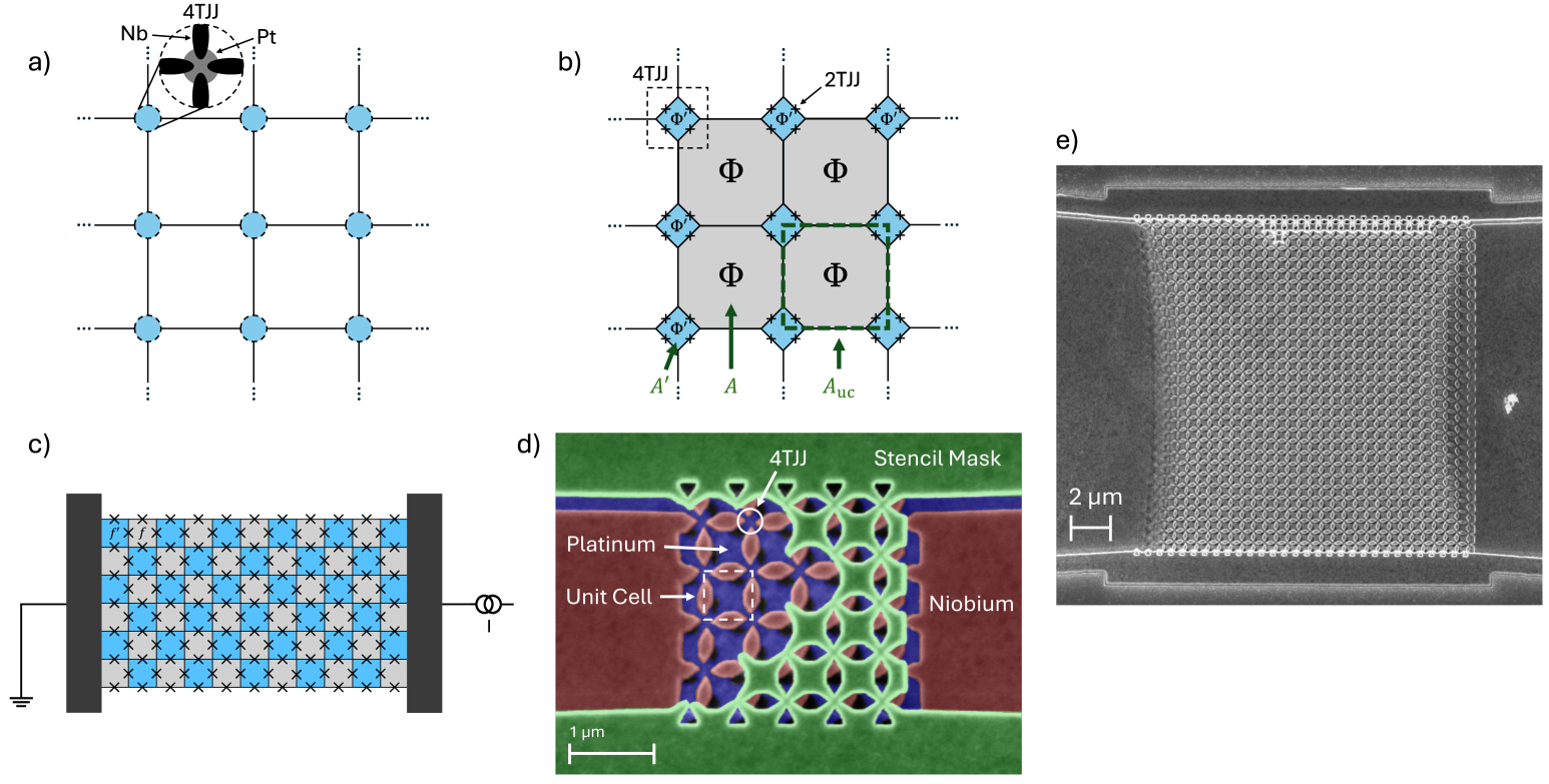
In contrast to conventional Josephson junction arrays, where a two-terminal Josephson junction (2TJJ) is placed in each arm forming a plaquette of the array, here a four-terminal Josephson junction (4TJJ) is situated in each corner of the plaquette. We aim to use the overlap between the two fields, arrays and multi-terminal Josephson junctions, to generate new knowledge for both of them.
We investigate Josephson junction arrays with a 4TJJ in each corner of a plaquette forming the array. Our 4TJJs are based on superconductor/normal conductor structure, using a metal as a weak link between the superconducting electrodes [1, 2, 29, 10, 30, 13]. More specifically, we use Nb for the four closely spaced superconducting electrodes connected by a metallic Pt weak link. The manufacturing process of the 4TJJ array is based on a stencil lithography process using molecular beam epitaxy with a high device yield [31]. The shadow evaporation based fabrication scheme employed here also ensures ultra-clean interfaces between the Nb and Pt layers. The periodic features in the magnetoresistance of a 4TJJ array are investigated in detail taking into account the magnetic flux penetrating each plaquette and the flux in the weak link area of the 4TJJ. The experimental results are supported by numerical simulations based on the resistively capacitively shunted junction (RCSJ) model, where the 4TJJ at each crossing point of the array is modelled by four interconnected two-terminal junctions, as illustrated in Fig 1 b).
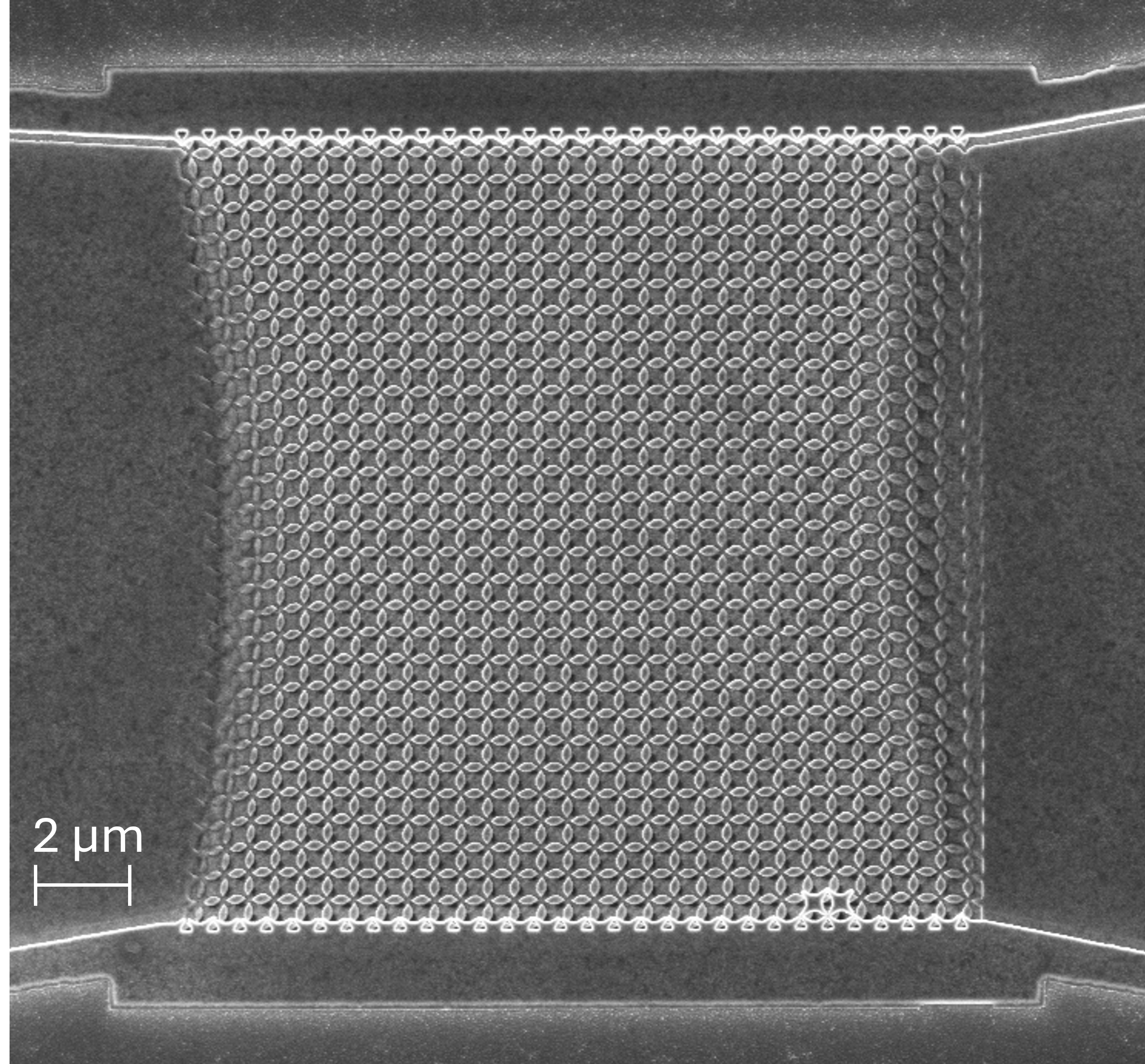
The stencil lithography fabrication process of the 4TJJ array with molecular beam epitaxy is described in the following. As a first step, a Si(111) substrate is covered by a 300-nm-thick SiO2 layer followed by a 100-nm-thick Si3N4 layer. Subsequently, the stencil mask is patterned into the Si3N4 layer by electron beam lithography and reactive ion etching. As a next step, the stencil mask is under-etched by hydrofluoric acid, removing the SiO2 layer below and revealing the Si(111) substrate surface. The stencil mask can be seen in Fig. 1 d).
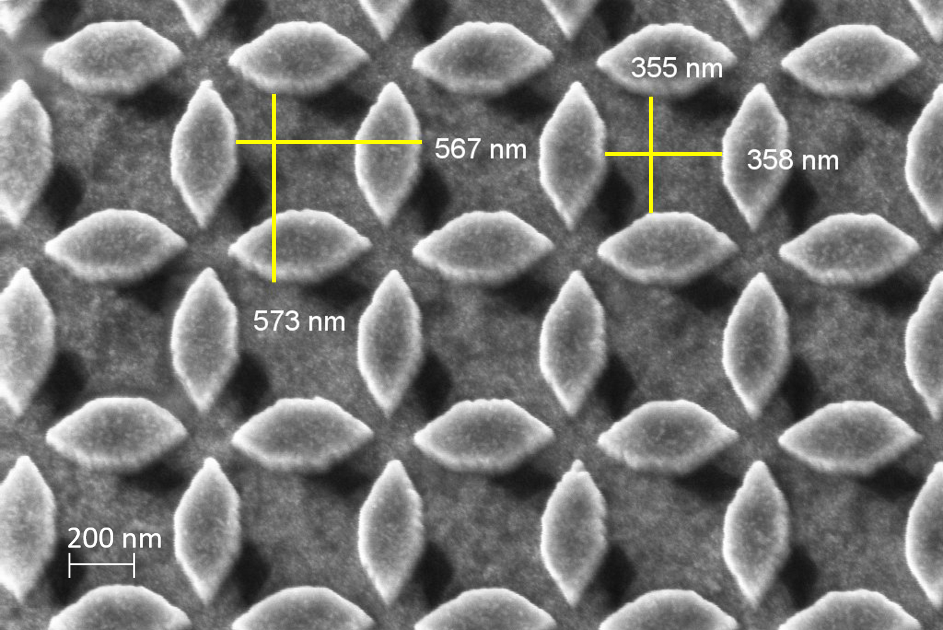
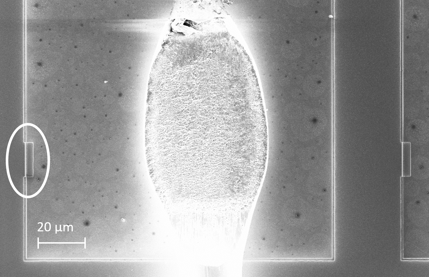
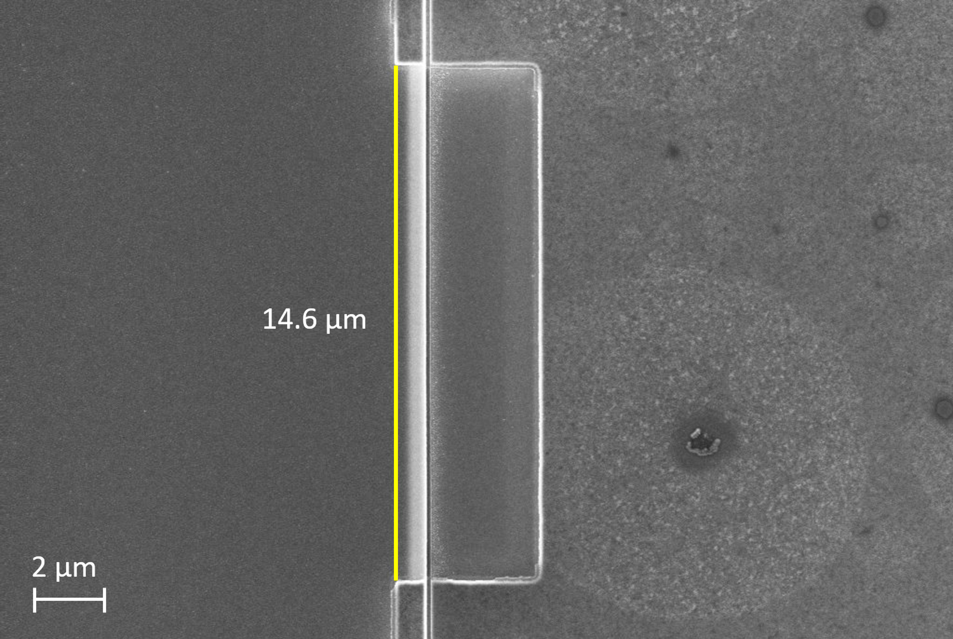
After inserting the pre-patterned substrate into an ultra high vacuum growth chamber, a 10-nm-thick Al2O3 interlayer is first deposited under rotation. The rotation ensures that the junction array area is completely covered by Al2O3. Next, a 20-nm-thick Pt layer is deposited under rotation. Here, the deposition at different angles due to the substrate rotation results in the deposition of Pt connecting the openings of the stencil mask. Finally, a 50-nm-thick superconducting Nb layer is deposited without rotation, resulting in a Nb electrode pattern defined by the opening of the stencil mask. As a last step, a 5-nm-thick Al2O3 capping layer is deposited under rotation. In Fig. 1 d) a scanning electron microscope image of the final device structure is shown. The four-terminal Josephson junction consists of four superconducting Nb islands connected at their tips by a central Pt weak link area. After the material deposition, the stencil mask is removed by applying ultrasonic power. The square unit cell of the array formed by a 4TJJ in each corner is indicated in Fig. 1 d). To prevent screening of magnetic fluxes by screening currents in superconducting material surrounding the array, the Nb layer outside the device is removed by reactive ion etching. Figure 1 e) shows a scanning electron microscope image of the 3030 4TJJ array investigated in this study. In addition to the device presented in the main text, we measured an identical array device and a reference two-terminal Josephson junction, all fabricated on the same substrate during the same fabrication run, presented in the supplementary material.
The measurements have been performed in a dilution refrigerator with a base temperature of 70 mK equipped with a superconducting magnet. For measurements with magnetic fields below 80 mT, an external high-resolution current source was used to supply the bias current of the magnet. The voltage signal, from which the resistance () and differential resistance () has been calculated, was measured with a quasi 4-point setup by applying a dc bias to the array. In additional measurements, the dc signal was superimposed with a smaller AC signal in order to measure the differential resistance using the lock-in technique (see supplementary material).
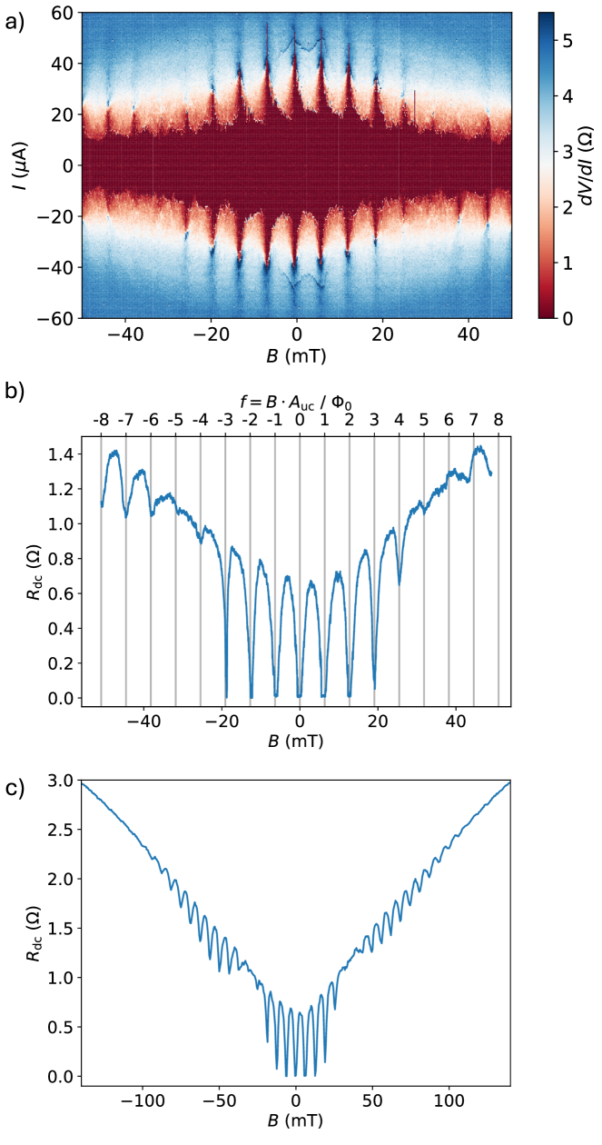
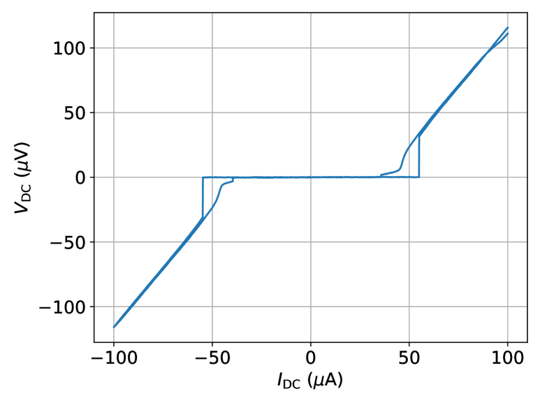
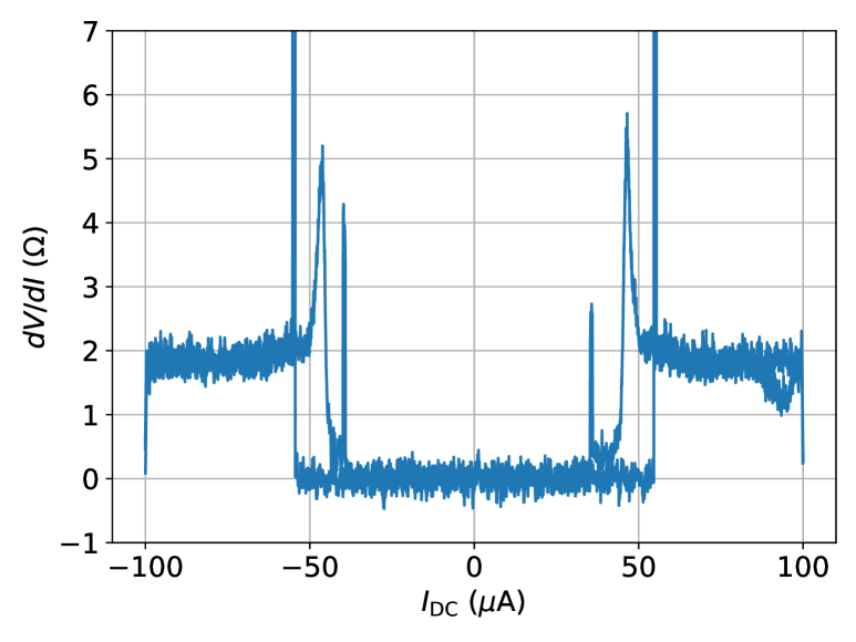
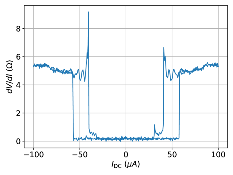
Magnetotransport measurements have been performed on a 4TJJ array at a temperature of 80 mK. At zero magnetic field, the array shows a critical current of A and, close to the superconducting regime, the device has a differential resistance of around 5.5 (see supplementary material).
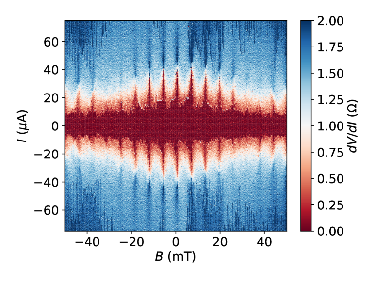
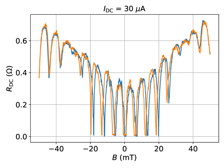
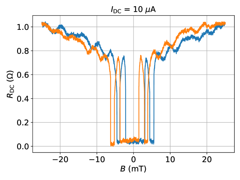
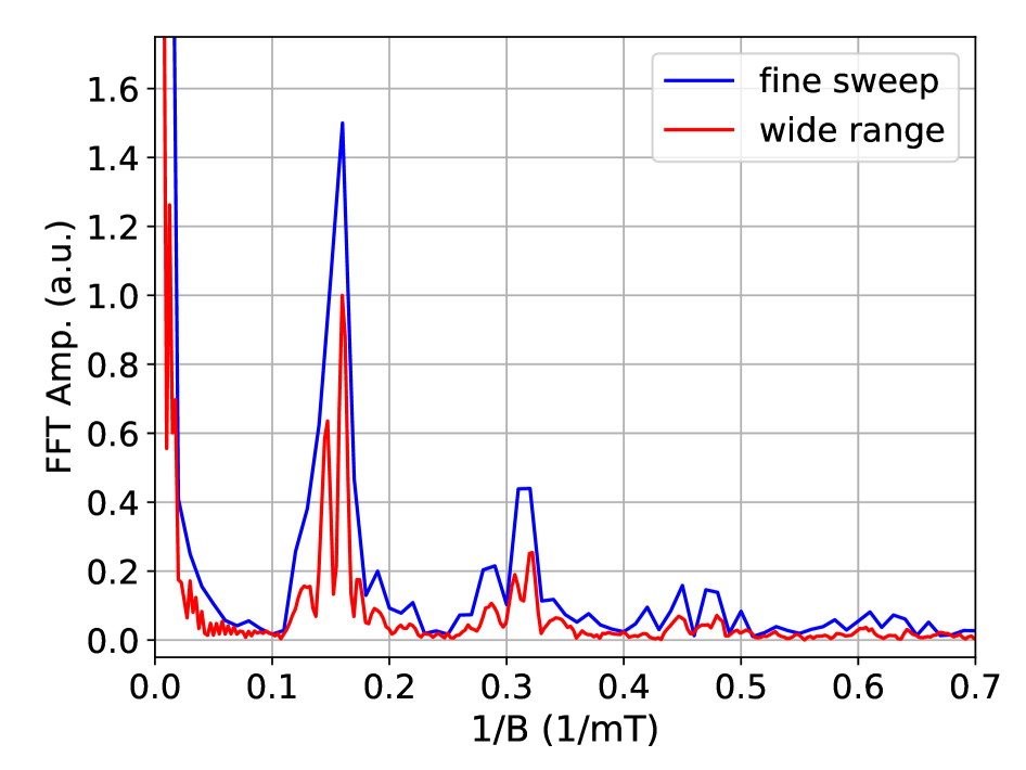
The differential resistance-bias current-magnetic field diagram depicted in Fig. 2 a) shows periodic oscillations of the critical current with magnetic field. When applying a direct current of 30 A through the device, its resistance oscillates with the same periodicity in magnetic field (cf. Fig. 2 b), which was determined to be 6.25 mT by a fast Fourier transform (see supplementary material). In addition, a device- and array-independent (present in the reference 2TJJ and both arrays) magnetic hysteresis of the resistance pattern was measured, which is not further considered in the main text (see supplementary material).
To describe the properties of Josephson junction arrays, the so-called frustration parameter , with being the array unit cell, the magnetic field strength perpendicular to the array plane, and the magnetic flux quantum, is widely used to characterize the magnetic resistance pattern, i.e. frustration pattern, see e.g. Refs. [2, 11]. It describes the average number of flux quanta piercing though an array unit cell. For rescaling the magnetic field into frustration, the unit cell area, as indicated in Figs. 1 d), has been determined to be nm by scanning electron microscopy (see supplementary material). It is important to note that this unit cell is the sum of a large unit cell area () and a small unit cell area () of Fig. 1 b), . The flux quantum oscillations of the resistance fit to in Fig. 2 b).
The resistance signal is similar to what, e.g. Rzchowski et al. [2] measured, however, the expected frustration pattern for rational values of is missing. As can be seen in Fig. 2 c), at certain magnetic field around , the oscillations first disappear and then reappear when further increasing the magnetic field. As will be explained below, both features, the different frustration pattern and the beating pattern, stem from the altered array lattice, which can be described by a conventional 2TJJ square lattice with checker board flux pattern. This gives rise to a superimposed beating pattern in addition to the flux quantum oscillations of the array unit cell. The periodicity of that beating pattern is approximately equal to the area ratio of the large array unit cell () and the 4TJJ central weak link region (). The base offset of the resistance dips can be explained by the Fraunhofer effect of the 2TJJs between two individual contacts of a 4TJJ. The resistance oscillations can be seen to magnetic fields above mT with, in total, 30 flux quantum oscillations ().
To explain the measured behavior of the 4TJJ array, a corresponding theoretical model is introduced in the following. The experimental device is schematically depicted in Fig. 1 a). Its square unit cell has one 4TJJ in each corner. The junctions are connected via their superconducting Nb contacts and every junction has a central Pt weak link region. Based on the RCSJ network model for multi-terminal Josephson junctions [28], the array can be described as shown in Fig. 1 b) with four 2TJJs creating one 4TJJ (see also supplementary material). This introduces a second lattice of areas pierced by magnetic flux, the central weak link region of the 4TJJs.
The multi-terminal array model as shown schematically in Figs. 1 a) and b) can be conveniently represented in terms of an ordinary square lattice junction model [see Fig. 1 c)], with the following important difference to previous theoretical and experimental studies: instead of all the plaquettes being pierced by the same flux, we get an alternating (checker board) flux pattern ( and ). We capture the dynamics of this system by means of a classical RCSJ model approach, where the equations of motion for the superconducting phases at nodes follow as usual from the Kirchhoff laws (for more details see supplementary material).
Including a source and drain contact on two sides of the lattice, the RCSJ model allows for a direct computation of the dc resistance as a function of the magnetic field. We do so by an explicit numerical evaluation of the classical RCSJ equations of motion. In addition we track the state of the system by a quantity related to the more commonly considered vorticity [4]: for a given plaquette, we calculate the counter clockwise supercurrent in the loop defining the plaquette (where for two neighbouring circuit nodes , the supercurrent is given as with the equivalent of the Peierl’s phase capturing the magnetic flux), see also Fig. 3 a). This loop current captures the vortex structure qualitatively quite well, see, e.g., the loop current texture of the regular square lattice system for in Figs. 3 b) and c). Contrary to the vorticity however, the loop current does not return an integer number. This property will turn out to be useful in a moment, to describe stable states for the checker board flux system, .
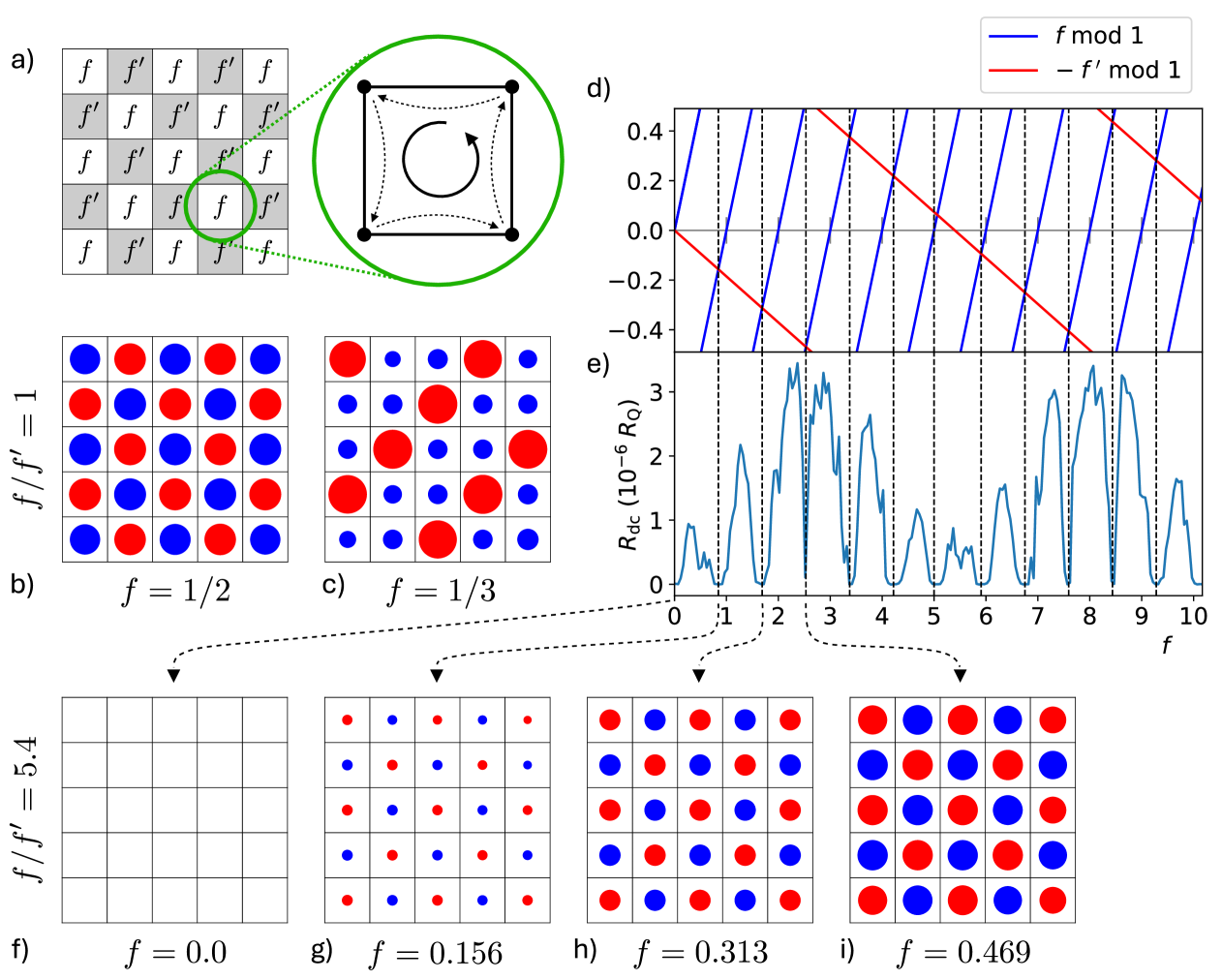
That being said, we explicitly compute as a function of for a square lattice with nodes 111The theory modelling occurs with a smaller system compared to the actual experimental setup. We do so simply to reduce the computational effort; the qualitative features of the theory model do not depend strongly on system size. for , yielding Fig. 3 e). The central finding is this: the dc resistance experiences superconducting dips whenever modulus , see Fig. 3 d). Consequently, while the flux through a single plaquette is far from being zero at a given dip (or an integer of the flux quantum), the sum of two neighbouring plaquettes is. Denoting the ratio , these dips occur for with . Since is given by the area ratio (see discussion of the experimental section above), is in general an irrational number, such that the dips in likewise occur at irrational values, . This is in stark contrast to regular square lattices commonly considered in previous works (), where dips at integer , with weaker side dips for rational with low denominator. In addition to the dips repeating with period in space, there is an overall beating pattern due to the fact that there repeatedly occur configurations where both and (value of at the dip) return to a value close to zero (up to modulus ), where we approximately recover the state at zero applied field. The period for that pattern is , where, due to (large discrepancy between two relevant areas in experimental setup) . This finding agrees very well with the experimental data shown in Figs. 2 b) and c).
When converting the frustration dip periodicity into magnetic field dip periodicity (6.25 mT) with and simplifying, we find . This result agrees with Fig. 2 b). In case that and are unknown, one can use the the difference in periodicities to estimate . Here, a value of was determined (see supplementary material). The area of the central weak link region is given by , resulting in
| (1) |
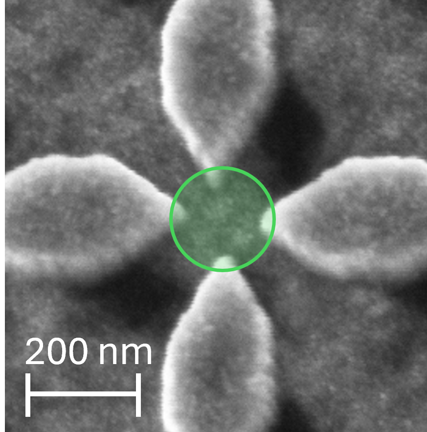
With this, the central weak link region of the 4TJJs is . This is compatible with the 4TJJ geometry (see supplementary material).
The only feature that is not captured is the base offset of the resistance dips that occurs for some finite magnetic fields (the fact that the dips return to a finite value instead of zero). This extra phenomenology can however be explained very easily: the above deployed RCSJ model assumes critical currents for the individual junctions that are independent of the magnetic field. In reality, given the estimated areas of the junctions, there is a finite onset of a Fraunhofer pattern, reducing the critical current at stronger magnetic fields (Fig. 2 a). When biasing the array with a constant current and ramping the magnetic field, this results in the finite-value- instead of zero-resistance dips.
Ultimately, the checker board arrangement of alternating fluxes () provides a unique opportunity to stabilize the superconducting (insulating) phase of the Berezinskii–Kosterlitz–Thouless (BKT) transition for incommensurate (irrational) flux quanta, since two neighbouring plaquettes can be tuned to values that cancel (up to modulus ) over a unit cell containing two plaquettes. The insulating phase of the vortex BKT transition corresponds to a superconducting phase in terms of the transport properties (which is why we refer to this phase as the superconducting phase for the remainder of this work). The special feature of stabilizing the superconducting phase for incommensurate (irrational) flux quanta motivates us to study the stationary system state (at zero bias current) at the values where (suppressed vortex motion). Due to the irrational values for , the (integer-valued) vorticity is not well-suited for such an analysis. This is why we instead compute the steady state configuration of the previously introduced loop currents in Figs. 3 f)-i). Even though , the unit cell of the stationary state is always of the size of two plaquettes, due to cancelling – in contrast to, e.g., the regular state, which repeats over three plaquettes. In fact, the loop current texture of the respective stationary states gradually changes between the regular state (when both and are roughly integer) and the regular state (note that for half-integer flux quanta, is equivalent to , hence the checker board state with is here indistinguishable from ). The here presented work thus provides a glimpse into classes of states that have not been investigated so far. While the dips at the beginning and the end of a beating pattern (period ) correspond very closely to the regular states integer, the dip in the middle of the beating period corresponds to – thus evidencing a regular frustration pattern. The dips in between provide states that defy the usual frustration picture as they occur at flux values far away from rational flux quanta. Therefore, we can think of the checker board arrangement with incommensurate ratio as a way to circumvent usual frustration.
Finally, the above finding can be cast into the more commonly used language of vortices and the BKT transition. The energy of the classical 2D Josephson junction array in terms of the number of vortices per plaquette is given by (see, e.g., Ref. [9] for details),
| (2) |
where the indices address the plaquette positions in 2 dimensions (i.e., both and implicitly encode a pair of and coordinates), and represents the typical logarithmic long-range interaction. For regular square lattices (i.e., all plaquettes experience the same flux), the well-known BKT picture arises. At zero flux , the zero vortex state (which is insulating in that no vortices are available to move) corresponds to the ground state, whereas states with finite vortex numbers or vortex pairs (conducting states) are at low temperatures inaccessible due to a finite energy gap, leading to the BKT transition. At finite flux, e.g., , the system reacts in such a way that the new ground state can be to a good approximation described by a state with a finite vortex density of vortices per plaquette, in order to screen the applied external flux, where (as is well-known) the propensity of the ground state to have ordered (and thus likewise insulating) vortex configurations or many freely moving vortex configurations depends on whether is a rational number or not.
For the here present checker board flux texture ( for alternating plaquette positions) the situation is different in the following crucial aspect. The aforementioned special points of cancelling neighbouring fluxes still have the zero vortex state as the gapped ground state because averaged over the whole system, no flux is applied, and hence no finite vortex density occurs due to screening. We therefore arrive again at the superconducting BKT phase, notably, at generally irrational values of . We emphasise that these zero flux states are by no means trivial. Consider the special (rational) case of and , with the zero vortex ground state. With a simple unitary transformation (increasing the vortex number on every plaquette by one), we map to the regular square lattice with the well-known ground state given by an alternating vortex configuration. Consequently, with the zero vortex ground state and with alternating vortex ground state are equivalent. Now, the difference to the case where but irrational (or in fact any rational or irrational number other than or ) is that the correspondence to the regular lattice is no longer exact (as there exists no unitary mapping due to ). For values close to , there still exists a unitary map to a system approximately equivalent to , this correspondence grows weaker and weaker as we move away from , which at the value of or lower leads to a cross over, where the checker board system with more closely imitates the regular system instead of . This constitutes a vortex perspective which is ultimately equivalent to the above analysis in terms of superconducting loop current configurations changing from the to the ground state [see also Figs. 3 f)-i) and their discussion above].
We demonstrated an array made with 4TJJs. For this we introduced an in-situ fabrication technique for array fabrication. A frustration pattern was measured which differs from the expectation for ordinary 2TJJ arrays. The difference could be explained by theoretically introducing a checker board lattice with two alternating flux patterns and . The periodicity of the beating pattern can be connected to the area ratios /. In particular, while dips in the dc resistance can be linked to the sum being integer, the in general irrational area ratio leads to an irrational repartition of this total flux into the alternating plaquettes. This allows for the stabilization of the superconducting BKT phase at irrational fractions of flux penetrating individual plaquettes – a feature we termed frustrated frustration. This feature allows us to estimate the spatial expansion of the 4TJJ central weak link region, the result of which is compatible with the junction geometry. Overall, the here considered setup opens up a previously unexplored class of array system with alternating flux textures. Given that detailed understanding of vortex lattice structures and their dynamics are still an open question for regular lattices with a single flux [9], the here introduced alternating lattice will likely lead to a rich catalogue of open research directions of its own, the full extent of which we could not possibly anticipate at this stage. As an example of a practical near-term question, we expect that at lower critical currents it might be perceivable to measure signatures related to rational (instead of integer) values of the sum , leading to substructures within the beating pattern profile. Also, non-local (e.g., multi-terminal) transport on such arrays, as well as their Shapiro response, could reveal further information about any nontrivial vortex configuration or motion.
We thank Herbert Kertz for technical assistance. All samples have been prepared at the Helmholtz Nano Facility [33]. This work is funded by the Deutsche Forschungsgemeinschaft (DFG, German Research Foundation) under Germany’s Excellence Strategy – Cluster of Excellence Matter and Light for Quantum Computing (ML4Q) EXC 2004/1 – 390534769, by the German Federal Ministry of Education and Research (BMBF) via the Quantum Futur project ‘MajoranaChips’ (Grant No. 13N15264), as well as the Bavarian Ministry of Economic Affairs, Regional Development and Energy within Bavaria’s High-Tech Agenda Project ”Bausteine für das Quantencomputing auf Basis topologischer Materialien mit experimentellen und theoretischen Ansätzen” (grant no. 07 02/686 58/1/21 1/22 2/23).
References
- H. Sanchez and Berchier [1981] D. H. Sanchez and J.-L. Berchier, Journal of Low Temperature Physics 43, 65 (1981).
- Rzchowski et al. [1990] M. S. Rzchowski, S. P. Benz, M. Tinkham, and C. J. Lobb, Physical Review B 42, 2041 (1990).
- Newrock et al. [2000] R. Newrock, C. Lobb, U. Geigenmüller, and M. Octavio, in Solid State Physics, Vol. 54 (Elsevier, 2000) pp. 263–512.
- Geigenmüller et al. [1993] U. Geigenmüller, C. J. Lobb, and C. B. Whan, Physical Review B 47, 348 (1993).
- Dang and Györffy [1993] E. K. F. Dang and B. L. Györffy, Physical Review B 47, 3290 (1993).
- Martinoli and Leemann [2000] P. Martinoli and C. Leemann, Journal of Low Temperature Physics 118, 699 (2000).
- Teitel and Jayaprakash [1983] S. Teitel and C. Jayaprakash, Physical Review Letters 51, 1999 (1983).
- Bozkurt et al. [2023] A. M. Bozkurt, J. Brookman, V. Fatemi, and A. R. Akhmerov, SciPost Physics 15, 204 (2023).
- Penner et al. [2023] A.-G. Penner, K. Flensberg, L. I. Glazman, and F. von Oppen, Physical Review Letters 131, 206001 (2023).
- Panghotra et al. [2020] R. Panghotra, B. Raes, C. C. de Souza Silva, I. Cools, W. Keijers, J. E. Scheerder, V. V. Moshchalkov, and J. Van de Vondel, Communications Physics 3, 1 (2020).
- Song et al. [2023] X. Song, S. Suresh Babu, Y. Bai, D. S. Golubev, I. Burkova, A. Romanov, E. Ilin, J. N. Eckstein, and A. Bezryadin, Communications Physics 6, 177 (2023).
- Bøttcher et al. [2023] C. G. L. Bøttcher, F. Nichele, J. Shabani, C. J. Palmstrøm, and C. M. Marcus, Physical Review B 108, 134517 (2023).
- Vervoort et al. [2024] S. Vervoort, L. Nulens, D. A. D. Chaves, H. Dausy, S. Reniers, M. Abouelela, I. P. C. Cools, A. V. Silhanek, M. J. V. Bael, B. Raes, and J. V. de Vondel, DC-operated Josephson junction arrays as a cryogenic on-chip microwave measurement platform (2024), arXiv:2412.17576 [cond-mat] .
- Pankratova et al. [2020] N. Pankratova, H. Lee, R. Kuzmin, K. Wickramasinghe, W. Mayer, J. Yuan, M. G. Vavilov, J. Shabani, and V. E. Manucharyan, Physical Review X 10, 031051 (2020).
- Riwar et al. [2016] R.-P. Riwar, M. Houzet, J. S. Meyer, and Y. V. Nazarov, Nature Communications 7, 11167 (2016).
- Graziano et al. [2022] G. V. Graziano, M. Gupta, M. Pendharkar, J. T. Dong, C. P. Dempsey, C. Palmstrøm, and V. S. Pribiag, Nature Communications 13, 5933 (2022).
- Coraiola et al. [2023] M. Coraiola, D. Z. Haxell, D. Sabonis, H. Weisbrich, A. E. Svetogorov, M. Hinderling, S. C. ten Kate, E. Cheah, F. Krizek, R. Schott, W. Wegscheider, J. C. Cuevas, W. Belzig, and F. Nichele, Nature Communications 14, 6784 (2023).
- Gupta et al. [2023] M. Gupta, G. V. Graziano, M. Pendharkar, J. T. Dong, C. P. Dempsey, C. Palmstrøm, and V. S. Pribiag, Nature Communications 14, 3078 (2023).
- Coraiola et al. [2024] M. Coraiola, A. E. Svetogorov, D. Z. Haxell, D. Sabonis, M. Hinderling, S. C. Ten Kate, E. Cheah, F. Krizek, R. Schott, W. Wegscheider, J. C. Cuevas, W. Belzig, and F. Nichele, ACS Nano 18, 9221 (2024).
- Gupta et al. [2024] M. Gupta, V. Khade, C. Riggert, L. Shani, G. Menning, P. Lueb, J. Jung, R. Mélin, E. P. A. M. Bakkers, and V. S. Pribiag, Nano Letters 24, 13903 (2024), arXiv:2312.17703 [cond-mat] .
- Kölzer et al. [2023] J. Kölzer, A. R. Jalil, D. Rosenbach, L. Arndt, G. Mussler, P. Schüffelgen, D. Grützmacher, H. Lüth, and T. Schäpers, Nanomaterials 13, 293 (2023).
- Behner et al. [2024] G. Behner, A. R. Jalil, A. Rupp, H. Lüth, D. Grützmacher, and T. Schäpers, Superconductive coupling and Josephson diode effect in selectively-grown topological insulator based three-terminal junctions (2024), arXiv:2410.19311 [cond-mat] .
- Kudriashov et al. [2025] A. Kudriashov, X. Zhou, R. A. Hovhannisyan, A. Frolov, L. Elesin, Y. Wang, E. V. Zharkova, T. Taniguchi, K. Watanabe, L. A. Yashina, Z. Liu, X. Zhou, K. S. Novoselov, and D. A. Bandurin, Non-Reciprocal Current-Phase Relation and Superconducting Diode Effect in Topological-Insulator-Based Josephson Junctions (2025), arXiv:2502.08527 [cond-mat] .
- Nikodem et al. [2025] E. Nikodem, J. Schluck, M. Geier, M. Papaj, H. F. Legg, J. Feng, M. Bagchi, L. Fu, and Y. Ando, Large tunable Josephson diode effect in a side-contacted topological-insulator-nanowire junction (2025), arXiv:2412.16569 [cond-mat] .
- Fu and Kane [2008] L. Fu and C. L. Kane, Physical Review Letters 100, 096407 (2008).
- Van Heck et al. [2012] B. Van Heck, A. R. Akhmerov, F. Hassler, M. Burrello, and C. W. J. Beenakker, New Journal of Physics 14, 035019 (2012).
- Fulga et al. [2013] I. C. Fulga, B. Van Heck, M. Burrello, and T. Hyart, Physical Review B 88, 155435 (2013).
- Graziano et al. [2020] G. V. Graziano, J. S. Lee, M. Pendharkar, C. J. Palmstrøm, and V. S. Pribiag, Physical Review B 101, 054510 (2020).
- Pfeffer et al. [2014] A. H. Pfeffer, J. E. Duvauchelle, H. Courtois, R. Mélin, D. Feinberg, and F. Lefloch, Physical Review B 90, 075401 (2014).
- Skryabina et al. [2017] O. V. Skryabina, S. V. Egorov, A. S. Goncharova, A. A. Klimenko, S. N. Kozlov, V. V. Ryazanov, S. V. Bakurskiy, M. Yu. Kupriyanov, A. A. Golubov, K. S. Napolskii, and V. S. Stolyarov, Applied Physics Letters 110, 222605 (2017).
- Schüffelgen et al. [2019] P. Schüffelgen, D. Rosenbach, C. Li, T. W. Schmitt, M. Schleenvoigt, A. R. Jalil, S. Schmitt, J. Kölzer, M. Wang, B. Bennemann, U. Parlak, L. Kibkalo, S. Trellenkamp, T. Grap, D. Meertens, M. Luysberg, G. Mussler, E. Berenschot, N. Tas, A. A. Golubov, A. Brinkman, T. Schäpers, and D. Grützmacher, Nature Nanotechnology 14, 825 (2019).
- Note [1] The theory modelling occurs with a smaller system compared to the actual experimental setup. We do so simply to reduce the computational effort; the qualitative features of the theory model do not depend strongly on system size.
- Albrecht et al. [2017] W. Albrecht, J. Moers, and B. Hermanns, Journal of large-scale research facilities JLSRF 3, A112 (2017).
Frustrated Frustration of Arrays with Four-Terminal Nb-Pt-Nb Josephson Junctions
(Supplementary Material)
SUPPLEMENTAL NOTE 1: Second 3030 4TJJ Array
In addition to the 3030 4TJJ array presented in the main text, there was a second device on the same sample. It equals the first in every aspect. Here, we present the data of the second 4TJJ array (see Fig. S1).
The critical current oscillates with magnetic field in the same way as for the main text array. With a DC bias of 30 A, that behavior leads to an oscillation of the resistance with magnetic field (see Fig. S4 b). Similar to the main text device, the frustrated frustration pattern is present. The damping of the oscillations of resistance and critical current can be reproduced.
At zero magnetic field and a temperature of 80 mK, the critical current is comparable to the main text device with A (see Fig. S1 c and d). The differential resistance is lower with close to the maximum applied current of 100 A.
SUPPLEMENTAL NOTE 2: Reference two-terminal Josephson junction
On the chip of the presented arrays, a reference two-terminal Josephson junction has been fabricated in the same way as the arrays (see figure S2). The weak link length was determined to be 92 nm and its width is 920 nm. Although only a width of 809 nm is indicated in figure S2, Pt and Nb material under the edge of the bottom Si3N4 layer needs to be taken into account. The angle between the substrate surface and niobium beam was 57.7∘. The 300 nm-thick-SiO2 layer right at the edge of the trench is etched away, just like under the mask itself. This leaves the 100 nm-thick-Si3N4 layer under-etched at the edge and gives additional substrate space for the niobium shadow to be deposited. The extent of the Nb shadow under the Si3N4 edge can be derived from the top shadow of image S2 (174 nm). The bottom shadow has a smaller distance from its edge than the top shadow because it is delimited by the lower edge of the Si3N4 layer (instead of the upper edge). That means that the bottom shadow will be shorter than the top shadow. This results in a total bottom shadow of 111 nm, which has already been added to the width specification of this Josephson junction above (920 nm).
In figure S2, the junction is shifted with respect to the stencil mask (by 42.2∘) because latter was rotated against the niobium beam during deposition.
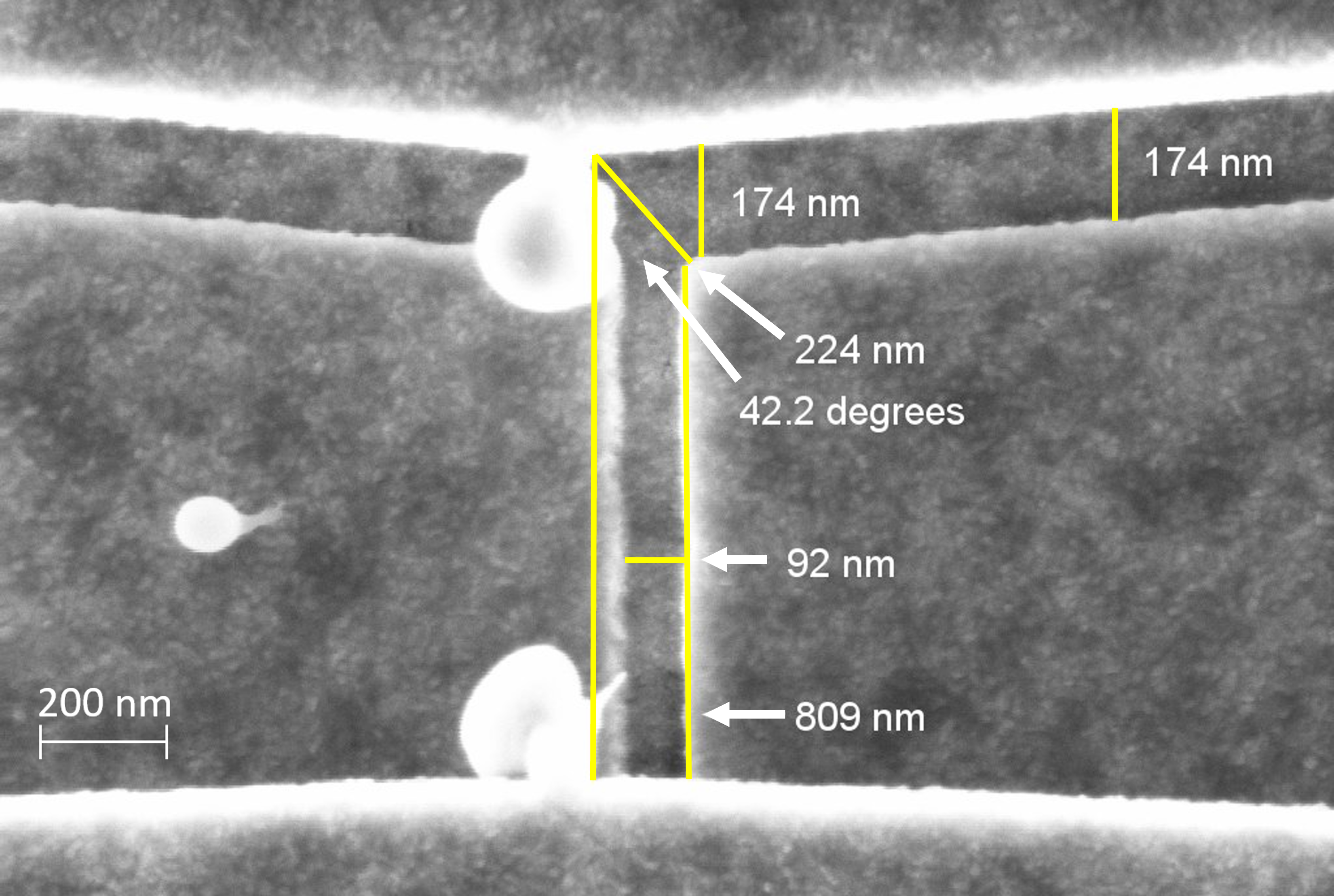
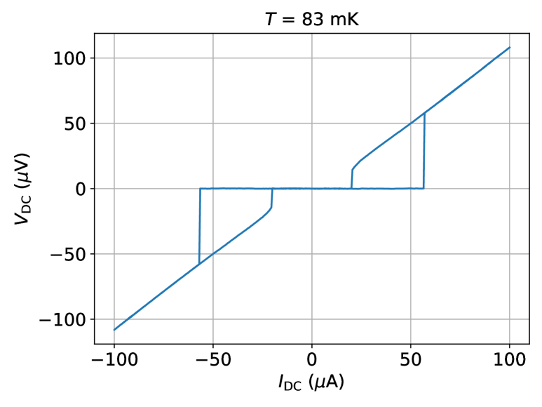
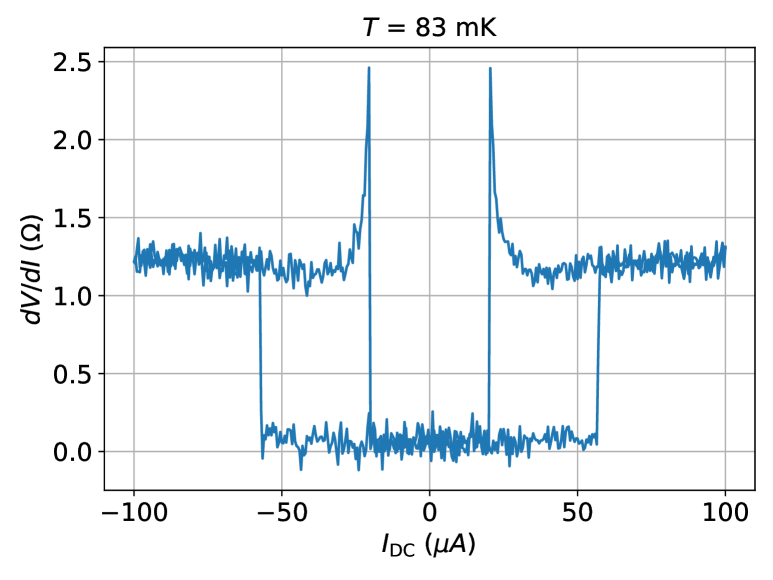
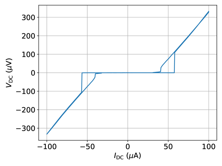
Figure S3 shows the voltage and differential resistance dependent on the current. The device has a critical current of 56.51 A and a differential resistance of 1.21 . The Josephson energy of the junction is meV. Using a relative permittivity of one (because platinum is a metal) and the geometrical values given above (length of a SC contact is 600 m), the coplanar junction capacitance is F.
Using the geometric device values, the device resistivity is nm and its critical current density is kA/mm2.
SUPPLEMENTAL NOTE 3: Magnetic hysteresis of the resistance pattern
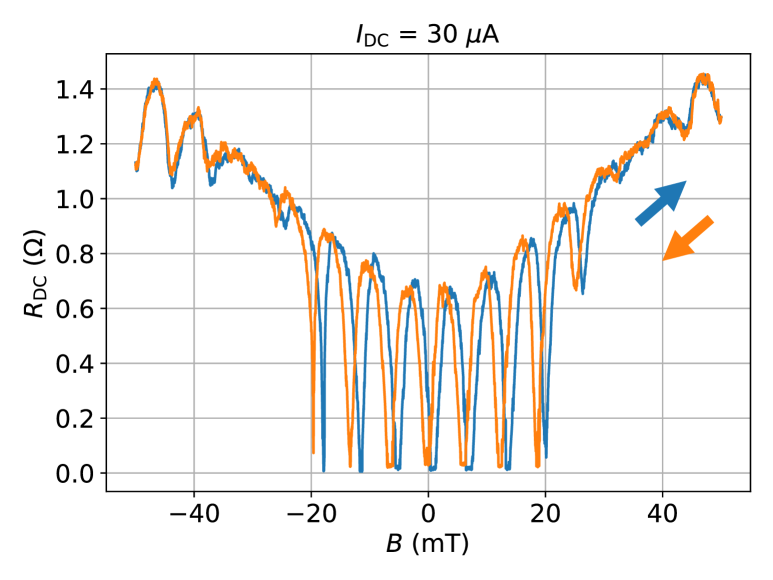
A magnetic hyteresis has been observed when measuring the resistance with magnetic field. The resistance oscillation pattern is shifted for different sweep directions of the magnetic field (see Fig. S4). The shift has been observed in all devices measured: In the arrays as well as in the two-terminal Josephson junction. Therefore, we rule out that the effect is device-specific. A possible reason is the screening of magnetic field by present Abrikosov vortices.
SUPPLEMENTAL NOTE 4: Determination of the resistance oscillation period
For the determination of the oscillation frequencies, fast Fourier transforms have been applied to the data in Fig. 3 c) and d) of the main text (see Fig. S5). The frequency spectra of both data curves match. The dominant frequency (period) is 0.16 1/mT (6.25 mT). The period of the beating pattern cannot be seen in the spectrum, probably because it is too close to the zero peak.
SUPPLEMENTAL NOTE 5: Description of the array device
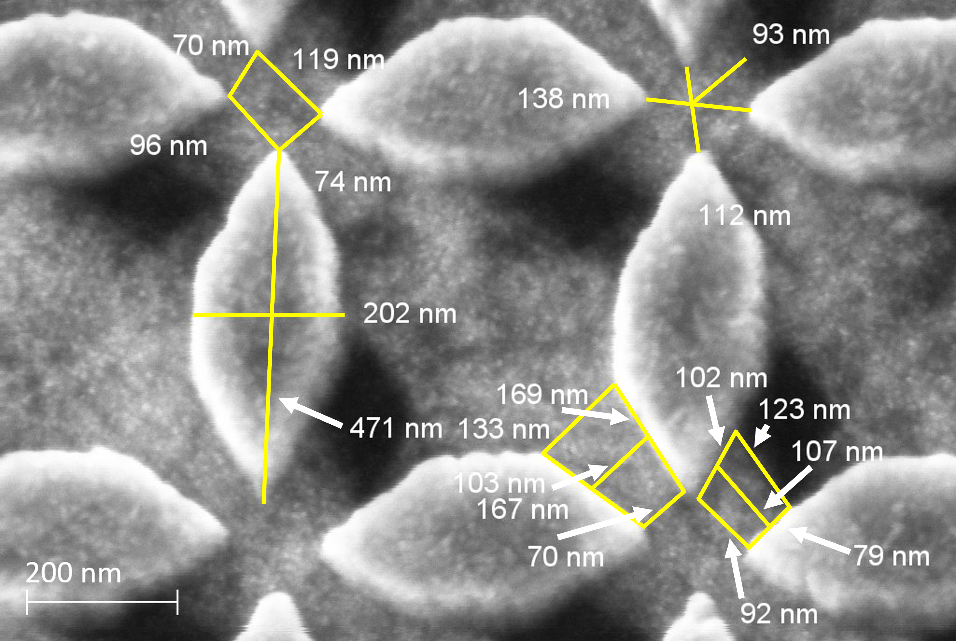
This section gives a detailed description of the array device in the main text, including geometrical properties of the array lattice (see Fig. S6). According to figure S6 a), the unit cell of the array is a square of size . The geometry of the weak link area between two neighboring leads of one 4TJJ (see Fig. S6 b) is described, on average, by the following dimensions: The width of the weak link is 129 nm and its length is 97 nm. The 4TJJ leads have a length of 471 nm.
During fabrication of the device, a trench is etched into the SiO2 (300 nm) / Si2N3 (100 nm) layer, down to the Si(111) substrate. On the substrate, the device is fabricated and, afterwards, the whole chip is covered with superconducting material. To minimize disturbance effects, the superconductor around the device is etched away as a last fabrication step, leaving an edge of superconductor of approximately 1 µm around the trench behind. To prevent this closed loop of superconductor from generating screening currents, the edge is disconnected close to the ends of the device contacts (see figure S6 c-d).
SUPPLEMENTAL NOTE 6: Characteristic RCSJ values between two leads of a 4TJJ in the arrray
In this section, relevant parameters for the theoretical description of the array are derived from geometrical considerations of the prior section, as well as from measurement data of the reference two-terminal Josephson junction. We assume that critical current density and resistivity, derived in section 2, are geometry independent. We then use these values, together with the 4TJJ geometry to derive capacitance, resistivity, and critical current between two leads of one 4TJJ.
The coplanar capacitance is calculated using the geometrical values given above. The relative permeability is assumed to be one, since the weak link is a metal. This results in a capacitance of F. The critical current between two 4TJJ leads is µA. This results in a Josephson energy of meV. The resistance is equal to .
SUPPLEMENTAL NOTE 7: Additional measurements of the main text 3030 4TJJ array
The current-voltage characteristics of the device presented in the main text can be seen in Fig. S7. The device has a critical current of A and a differential resistance of around 5.5 close to the maximum applied current of 100 A.
Additional measurements have been performed on the main text 3030 array device. Figure S8 shows temperature dependent IV curves. The declining critical current with increasing temperature is clearly visible.
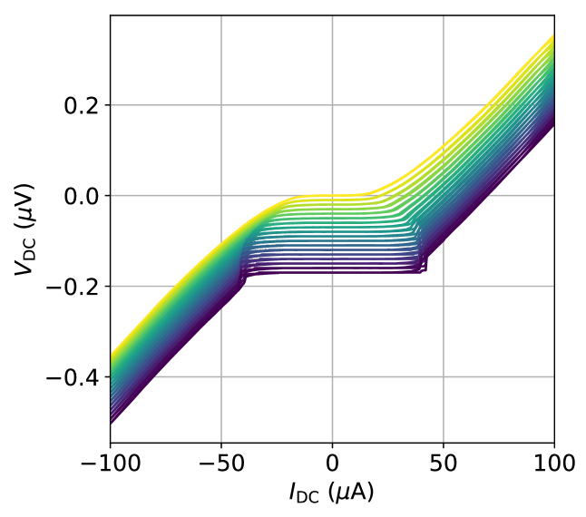
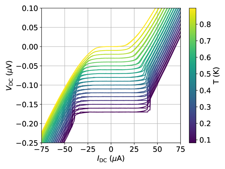
Figure S9 shows the same resistance oscillations with magnetic field as before but, here, they were measured with the AC lock-in technique and no DC bias. The resulting resistance is lower than with the DC measurement because the time-dependent sinusoidal signal includes the superconducting state of the device as well. When comparing figure S9 a) with figure S4 a), one can see that the oscillations are identical in magnetic field, although the peak pattern is more symmetrical with the AC method.
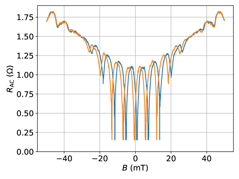
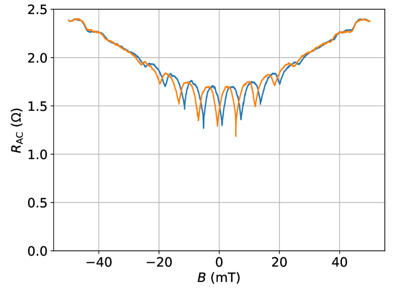
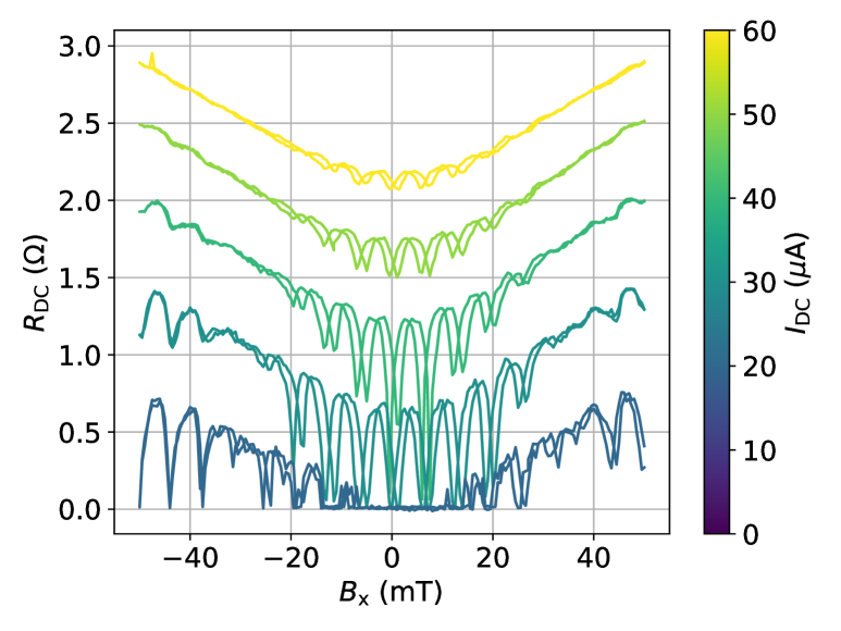
Figure LABEL:fig:SUPP_MISC_RB_DC_I_T a) shows resistance measurements dependent on magnetic field and DC current. At higher currents, superconductivity is not realized at any magnetic field and the oscillation amplitudes decline.
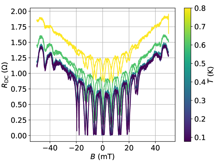
Figure LABEL:fig:SUPP_MISC_RB_DC_I_T b) shows resistance measurements dependent on magnetic field and temperature. At higher temperatures, superconductivity is not realized at any magnetic field and the oscillation amplitudes decline.
SUPPLEMENTAL NOTE 8: Details of the theoretical modelling
We here summarize the model calculations for the theoretical discussion of the main text. We describe the multiterminal Josephson junction array in the overdamped regime (discarding capacitive contributions), we get at each node the equation of motion,
| (S1) |
with shunt resistance , critical current , and the current noise term due to thermal fluctuations from the resistor connecting nodes and , where
| (S2) |
The notation indicates that the sum goes over nearest neighbours of .
SUPPLEMENTAL NOTE 9: Estimation of the central weak link area
According to the theoretical discussion in the main text, the parameter and the frustration dip periodicities are defined as:
| (S3) |
| (S4) |
| (S5) |
With this, the difference of the two periodicities can be estimated:
| (S6) |
For this estimate the was determined by counting the number of resistance dips between the two beating points in figure 2 c). Ten dips () can be seen between the two beating points. This yields and, thus, an estimated weak link area of .
For comparison, such a weak link area is sketched on one 4TJJ in Fig. S11, assuming the weak link region to be a perfect circle with the corresponding area of . As can be seen, a shape of this size is compatible with the 4TJJ geometry.