On the origin of bulk-related anisotropies in surface optical spectra
Abstract
Reflection anisotropy spectroscopy (RAS) is a powerful method for probing the optical properties of surfaces, used routinely in research and industrial applications, yet the origin of ’bulk-related’ features that appear in the spectra of various surfaces has been debated for nearly 40 years. It is often argued that these features are related to surface-induced bulk anisotropy (SIBA) because they coincide with critical energies of the bulk dielectric function. In general, any quantitative RAS theory must include excitonic effects as they significantly influence the spectra and are believed to be the key to determining the origin of SIBA features. Here, we introduce a layer-resolved exciton localization (LREL) measure within the framework of many-body perturbation theory, which enables a quantitative analysis of the origins of ’bulk-related’ RAS features. Applying LREL to arsenic-modified silicon reconstructions reveals that, depending on the surface reconstruction, the ’apparent’ SIBA features arise primarily from states localized at the surface, with only a small contribution from the underlying layers. Our findings, further supported by the fact that the calculated spectra agree well with low-temperature RAS measurements, challenge the conventional explanation of ’bulk-related’ RAS features. They indicate that in many instances bulk-enhanced surface anisotropies (BESA)—the opposite of SIBA—contribute to, or are even responsible for, ’bulk-related’ RAS features. Therefore, we suggest that previously studied semiconductor surfaces, which exhibit ’bulk-related’ features in their spectra, should be reanalyzed using the presented method.
I Introduction
Reflection anisotropy (RA) spectroscopy (RAS) has been extensively studied and discussed for a variety of semiconductor surfaces and heterostructures over the last decades due to its importance in surface characterization and technological applications [1, 2, 3, 4, 5, 6, 7, 8, 9, 10, 11, 12, 13, 8, 4, 14, 15, 16, 17, 18, 19, 20, 21, 22, 23, 24, 25, 26, 27, 28, 29, 30, 31]. However, the interpretation of RAS experiments has generally been far from straightforward, as RA spectra give only indirect insights into surface structure and chemistry. Furthermore, interpreting spectra based on simplified models, such as bond polarizability is difficult and may lead to wrong results [32]. Arguably, the full potential of RAS can therefore only be realized through a strong collaboration between experimental and theoretical work, especially in understanding the complex origins of the spectral features.
Today, RAS signatures due to transitions between surface states are well understood and have been enormously useful in surface exploration for decades, as reviewed in detail by Weightman et al. [33]. However, a topic that has been observed for many surfaces and has been heavily debated for the last 40 years (e.g., Refs. [1, 34, 35, 36, 37]) is the origin of ’bulk-related’ features in RA spectra, i.e., features that coincide with critical points of the imaginary part of the bulk dielectric function, also referred to as surface-induced bulk anisotropy (SIBA). Irrespective of the investigated surface or specific reconstruction, e.g, Si(100)-, Si(100)-:H and Si(100)-:H [23], Si(111):H and Si(110):H [24], GaAs(110) and GaAs(100)- [25], GaAs(100)- [26], As-rich GaAs(100)- [27], ZnTe(100) [28] and InP(100)- [29] the occurrence of SIBA features has been noted. Their origin is often argued to be related to ”bulk-like electronic states perturbed by the surface” [29]. Specifically, it has been proposed that they may be related to strain induced by surface reconstructions, steps or dimerization via the piezo-optic effect [24] or to surface electric fields via the linear electro-optic effect [31, 30]. Aspnes et al. [34] suggested that they are caused by photon-induced localization of bulk electronic states. In fact, some authors [25] have gone so far as to state: ”after realizing that many RA line shapes are similar to the imaginary part of the bulk dielectric function, or to its energy derivative, it is a growing belief that surface optical spectra are mostly determined by bulk effects, and therefore, not very useful as a tool of surface characterization.” While this sentiment has softened over the years, a clear explanation of SIBA features remains elusive.
From a theoretical point of view, it has long been recognized that excitonic effects, which are not captured by the independent particle approximation (IPA), contribute significantly to the RAS of semiconductor surfaces [5, 7, 20] and may be the key to explaining bulk-related features [25]. Nevertheless, only a limited number of studies [5, 7, 20, 23, 21, 22] have addressed these excitonic contributions by solving the Bethe-Salpeter equation (BSE) within the framework of many-body pertubation theory (MBPT) [38]. A detailed analysis of the excitonic transitions using BSE eigenvectors [39, 40] analogous to recent work on excitons near the bandgap of bulk or two-dimensional materials [41, 42, 43] remains to be fully explored for surfaces. The main challenge has been the computational cost associated with the exact diagonalization of the large, nonsparse BSE-Hamiltonian matrix [7, 20, 44]. As a result, previous investigations have either restricted the transition space, facilitated by a favorable surface band structure [5, 21], or employed iterative diagonalization algorithms [7, 20, 23], which yield the RAS without elucidating the underlying origins of the excitonic features. Even when the BSE was exactly diagonalized [22], a characterization of the excitonic features of RA spectra was not performed.
A detailed interpretation of excitonic features, especially for the aforementioned SIBA features, through a precise methodology would be particularly important for experiments monitoring RAS changes during sample growth or exposure experiments [45, 46, 47, 48]. To address this issue, we introduce the layer-resolved exciton localization (LREL) measure as a conceptual and quantitative framework for analyzing excitonic contributions to RA spectra. LREL combines the BSE eigenvectors with the state- and layer-resolved projected wavefunction characters, allowing us to specify from which atomic layer the excitonic contributions to the RAS originate.
While previous studies have been limited by the daunting computational demands of diagonalizing the BSE for surfaces, advances in high performance computing resources are finally making it possible to clarify the origin of the SIBA features: They allow us to accurately diagonalize the BSE and rigorously post-process the results using our LREL measure for large unit cells, i.e., the surfaces studied here. As a result, a detailed analysis of excitonic effects in semiconductor surfaces becomes possible, shedding light on the elusive origin of SIBA features. Thus, our study not only addresses a long-standing problem in the field, but also provides a recipe for the thorough analysis of surface optical spectra.
To test our method on a real system with a more challenging surface band structure than, for example, the Si(111)-() reconstruction [5], we focus on arsenic-modified Si(100) surfaces, which exhibit strong SIBA features. These surfaces have recently gained attention as a promising substrate for low-defect III-V-on-Si heteroepitaxy [51, 52, 53, 54, 55]. They have also been shown to be crucial for the development of low-cost, high-efficiency photoelectrochemical devices [56, 57, 58, 59].
We focus on two particular Si(100) reconstructions that form during arsenic exposure under different growth conditions. The first is the Si(100)-:As reconstruction with two symmetric As dimers, previously studied by Kipp et al. [3], which is formed during an ultra-high vacuum (UHV) preparation using As4 precursors [60, 3]. The second is the Si(100)-:As-Si-H reconstruction, which we have recently demonstrated to occur in chemical vapor deposition (CVD) environments, where large amounts of background hydrogen and hydrogen from tertiarybutylarsine (TBA) precursors lead to the formation of a reconstruction with mixed buckled As-Si-H dimers [61]. As experimental reference, we use data measured by Kipp et al. [3] at room temperature (RT) for the Si(100)-:As reconstruction and performed our own low-temperature (LT) RAS measurements for the Si(100)-:As-Si-H reconstruction, described in the Methods section. For the sake of brevity, we will omit from the notation of the surface reconstructions from now on, since all surfaces considered here share this unit cell.
Before introducing our analysis method and presenting results, we first outline and discuss the equations commonly used in the analysis of RA spectra. In general, RAS measures the difference between complex Fresnel reflection amplitudes along two orthogonal directions and in the surface plane of a sample.
| (1) |
Experimentally, the real part of the RAS is usually measured, i.e., , and often used directly for comparison with ab initio calculations for , which refer to the reflectivity . However, this direct comparison can lead to overestimated anisotropies because [62]. Taking into account this factor of two, we can calculate the RAS for normally incident light using the equation established in the works of Del Sole et al. [63, 64] and Manghi et al. [65]:
| (2) |
Here, is the bulk dielectric function of the substrate, and is the half-slab polarizability of the (reconstructed) surface. From an ab initio calculation of a symmetric surface slab approximating a semi-infinite crystal, is obtained from the difference of the diagonal components of the surface dielectric tensor , i.e., , where is half the thickness of the surface slab [65] and mirror symmetry or inversion symmetry is assumed [12]. From here on, we will refer to as the surface dielectric anisotropy.
At this point, it is beneficial to examine Eq. (2) in more detail to understand the effect of the bulk dielectric function on RA spectra. First, we decompose Eq. (2) into the real and imaginary parts of bulk and surface terms [66]
| (3) |
where
Obviously, the surface dielectric anisotropy can be strongly modulated by the bulk contributions and when the real part of the bulk dielectric is close to one while the imaginary part is small. For example, in bulk silver (see Fig. 4 in Ref. [17]), this phenomenon occurs around eV, which coincides with the point where the real part of the dielectric function approaches one, and still before the onset of the absorption peak is observed in the imaginary part. At this energy, remains relatively small.
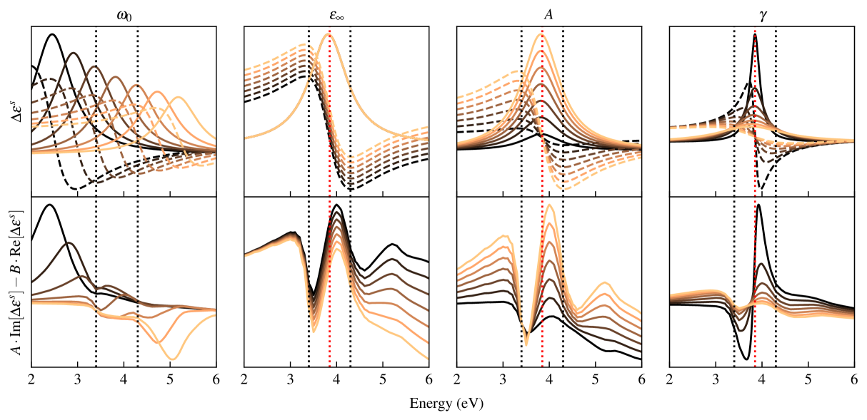
To further explore the influence of the bulk dielectric function on the RAS, we introduce a simple model system with silicon as the bulk (substrate) material. It illustrates explicitly that spectral features of a completely isotropic bulk material can show up as frequency-dependent reflection anisotropy of the surface!
In our model calculations, we systematically vary the surface dielectric anisotropy of a fictitious surface layer on top of isotropic bulk silicon. The latter is modeled via the dielectric function and , measured by Aspnes et al. [49]. We note in passing that the structures of and are similar to those of other common semiconductors such as Ge, GaAs, and GaP (see Ref. [66]). The surface dielectric anisotropy is modeled as a single Lorentz oscillator , with , i.e., , and we explore the influence of the four model parameters (, , , ) on the RAS. The numerical values of the model parameters and a visualization of and derived from the measured bulk dielectric function are given in the Supplementary Information, i.e., Supplementary Note 1. Our model can be interpreted as accounting for changes in the electronic structure at the surface of a semiconductor substrate, such as those resulting from changes in surface reconstruction due to varying growth conditions or the addition of a monolayer with anisotropic optical properties.
The model surface dielectric anisotropy and the resulting RAS, i.e., Eq. (3) without the prefactor , are shown in Fig. 1. Looking at the first column, where we vary while keeping the other parameter fixed, we see that the sign of the RAS changes depending on whether the surface dielectric anisotropy is below or above the critical points of the bulk dielectric function (indicated by the dotted black lines). When the peak of the surface dielectric anisotropy is at or between the critical points of the bulk dielectric function ( eV), a strong modulation of the RAS is seen, which could easily and erroneously be attributed to SIBA rather than to what could be called ’bulk-enhanced surface anisotropy’ (BESA). In columns 2-4 in Fig. 1, the other model parameters are varied, while keeping eV fixed (dotted red lines). Generally, negative peaks are observed near the critical points of the bulk dielectric function, and the strong (positive) peak attributed to the surface dielectric anisotropy is slightly blue-shifted. Varying the other model parameters while keeping fixed shows that the position of the surface dielectric anisotropy feature has the most significant influence on the RAS, while other parameters primarily affect the amplitude. In summary, the model results demonstrate that the surface dielectric anisotropy may be strongly modulated by the bulk dielectric function, depending on the relative position of bulk and surface spectral features. This interaction complicates the interpretation of RA spectra, especially when investigating SIBA features. Therefore, a more comprehensive analysis of RA spectra incorporating the surface dielectric anisotropy, derived from ab initio calculations is called for.
In an ab initio context and taking into account excitonic effects (electron-hole interactions), the surface dielectric anisotropy is calculated using the surface dielectric tensor, which is obtained here by solving the BSE in the Tamm-Dancoff approximation [67] as a generalized eigenvalue problem [40]. The diagonal components of the surface dielectric tensor are then calculated as follows:
| (4) |
where are the exciton excitation energies (BSE eigenvalues) and is the oscillator strength along axis . Here is a phenomenological broadening parameter that accounts for the finite lifetime and damping of excitonic states. In practice, this is just a small real number, see Methods. The oscillator strength is defined as:
| (5) |
where are the normalized excitonic wave function coefficients (BSE eigenvectors) obtained from a diagonalization of the BSE Hamiltonian [40] with , and is the unit cell volume. The sum in Eq. (5) runs over all considered vertical transitions from valence band to conduction at k-point . The quantity includes the transition matrix elements of the velocity operator along the Cartesian direction , the Fermi occupation function , and the Kohn-Sham states and eigenvalues () obtained from density functional theory (DFT) calculations.
In Eq. (5) we can see that for each exciton all considered single-particle transition matrix elements contribute with a weight corresponding to the associated normalized BSE eigenvectors . This complicates the assignment of spectral features to specific states considerably.
For this reason, fatband analyses of excitonic transitions are often employed in studies of bulk and two-dimensional materials (see, e.g., Fig. 2 in Ref. [42] and Fig. 3 in Ref. [43]). In these analyses, the ”fatness” (e.g., band thickness or marker size) of the valence and conduction bands is proportional to . In practice, one first selects a particular exciton state of interest, i.e., , and calculates for all transitions included in the BSE Hamiltonian. Then, for each transition (indexed by , , and ), the corresponding valence and conduction bands in the band structure are ”highlighted” proportional to . The highlighted Kohn-Sham (KS) states can then be assigned to individual atoms or specific orbitals by projecting them onto local orbitals, providing valuable insight into the structure of individual excitons. However, analyzing RA spectra in this way becomes impractical because, as will be seen later, many excitons often contribute to a specific spectral feature, rendering such an approach cumbersome and inefficient.
For this reason, we introduce the layer-resolved exciton localization (LREL) measure which is calculated for the valence bands (VB) as
| (6) |
where is the layer-resolved projected wave function character of the KS state . Here the index refers to a particular layer in the slab, not to be confused with the half-slab polarizability . For conduction bands (CB), is defined analogously with replaced by . Clearly, LREL quantifies the contribution of different layers in a slab to a given exciton. This is done by weighting the contributions of each layer to a state , i.e., , by how much that state contributes to excitons , i.e., , for all single-particle transitions considered.
Similar to the fatband analysis briefly described above, LREL now allows us to quantify how much each layer of a surface slab contributes to the exciton at energy . Since it involves only reciprocal space quantities, it is easy to compute even for many excitons without having to use, for example, high-dimensional excitonic wave functions on a real-space grid.
In this study, we calculate as follows: (i) We calculate the orbital- and site-projected partial wavefunction character of the KS state , i.e., with spherical harmonics centered on the ion , as implemented in the Vienna Ab-initio Simulation Package (VASP) [68, 69]. (ii) For each site , the sum over all orbitals is calculated. (iii) By summing the contributions of the individual atoms within the layer of the surface slab, we obtain . The top layer (hereafter referred to as S) corresponds to the surface reconstruction and consists of either As-As or As-Si-H dimers, depending on the reconstruction, while the other layers consist of two silicon atoms each.
It is important to keep in mind that the numerical values of the projections implicitly depend on several parameters, most notably the projection radii around the atomic sites. Here, the values set given by the projector augmented wave pseudopotentials [70] for each atomic species were used as projection radii, thereby ensuring consistency with the basis functions and maintaining accuracy without the need for manual adjustments. For any reasonable choice of projection radii, the LREL should be sufficiently accurate to allow quantitative analysis of the contributions of the different layers and thus insight into the spatial localization of excitonic effects without the need for more complex projection methods. To make it easier to interpret LREL for a fixed exciton , we introduce the normalized LREL
| (7) |
where . is now directly proportional to the percentage of how much layer contributes to the exciton . The calculation settings used to obtain are given in the Methods Section. Before we present the results, we note two almost trivial observations in passing: (i) Any other method of projecting a KS state onto localized orbitals, i.e., obtaining , can be used to calculate the LREL. (ii) The LREL can also be used to analyze RAS features in an atom- or orbital-resolved fashion by omitting the sum over all atoms in a layer or orbitals.
II Results
II.1 Electronic structure and optical properties
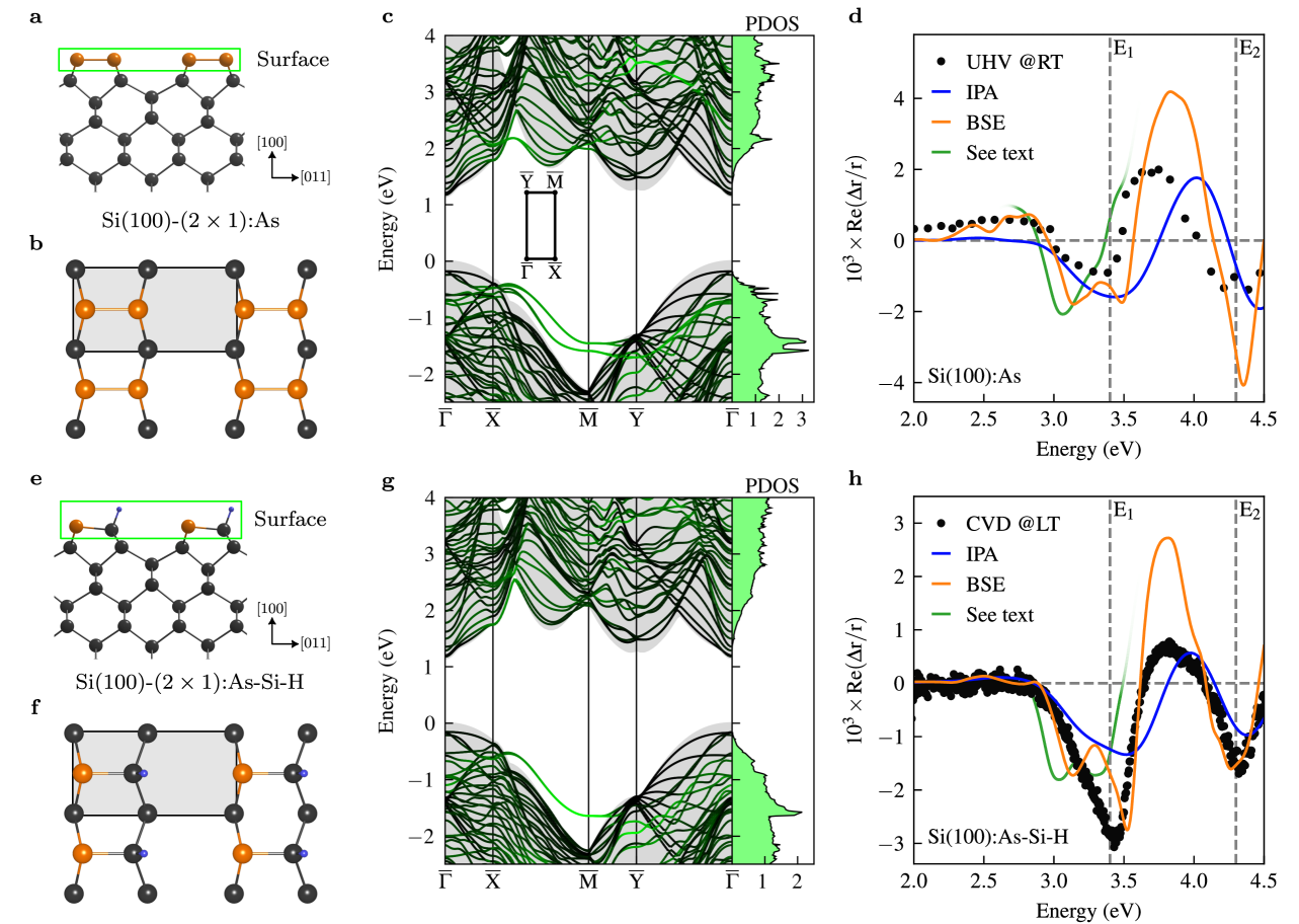
We begin by summarizing the structural, electronic, and optical properties of the Si(100):As and Si(100):As-Si-H surface reconstructions which we need for the subsequent excitonic analysis. Figure 2 provides an overview of the atomic arrangements, surface band structures, and RA spectra. The side and top views of the Si(100):As and Si(100):As-Si-H surface reconstructions, highlighting their similar yet distinct atomic configurations, are shown in Fig. 2a–b and Fig. 2e–f, respectively. Surface band structures calculated with the hybrid functional HSE06 (see Methods) are shown in Fig. 2c and g, where the bands are colored by to highlight the contributions from the surface (green). Both reconstructions exhibit surface states near the valence band manifold between the and points in the surface Brillouin zone. Comparing both, it can be observed that the surface states are directly related to the arsenic atom in the surface structure, as the Si(100):As with two As atoms shows two distinct surface bands, while the Si(100):As-Si-H with only one As atom shows one surface band. This observation is further supported by the Si(100):As-Si-H surface band structure shown in Supplementary Note 2, where the bands are colored by .
In Fig. 2d and h, we present the experimental and calculated RA spectra. The measured spectra of both reconstructions exhibit pronounced features at and that are also observed in measurements of other Si(100) reconstructions [23]. The origin of these features, often explained in terms of SIBA, will be investigated later. Comparing the measured RAS of the Si(100):As at RT with our LT RAS measurements of the Si(100):As-Si-H, we observe a slight blue shift and an increase in the feature amplitudes. This observation is more apparent when comparing the Si(100):As-Si-H measured at process temperatures with the LT measurements shown in Supplementary Note 6. The observed spectral changes in our LT measurements can be explained as follows: While thermal expansion causes only a small redshift of the indirect band gap of about meV shift when the temperature is increased from K to K in bulk silicon, electron-phonon interactions induce a substantial increase of the indirect band gap at LT of – eV [71], explaining the shift in peak positions. The reduction of exciton-phonon scattering at lower temperatures, confirmed by ab initio calculations for silicon and h-BN [72], leads to the observed reduced peak broadening, i.e., the increase of feature amplitudes. In addition, the increase in features amplitude in LT measurement is also likely enhanced by a higher surface order, increasing the anisotropy.
Having presented the experimental data, we now turn to the spectra obtained from the theory. The spectra shown are calculated using Eq. (2), where and are obtained from consistent theory levels starting from a HSE06 calculation, i.e., by calculating the IPA dielectric function or solving the BSE. As shown several times before [5, 7, 20, 23], we again observe that excitonic effects included in the BSE (orange) strongly modulate (red shift and line shape change) the RA spectra compared to IPA calculations (blue). The calculated BSE spectra closely match the experimental data. However, it could be argued that the BSE prediction for the Si(100):As surface reconstruction agrees with the measurement by Kipp et al. [3] not much better than the IPA spectra. This is likely due to the fact that the measurement was performed at RT, where excitonic effects are diminished and some degree of surface disorder may be present, reducing the optical anisotropy as discussed above. Comparing the two surface reconstructions, we notice a reversal in the amplitude ratio of the peaks at and , a trend also suggested by experimental data. However, a LT measurement of Si(100):As would be required to fully validate this theoretical observation. At this point, we need to comment on the double peak visible at in both BSE calculations (orange lines in Fig. 2d and h). A similar feature has been observed and extensively discussed by Albrecht et al. [73] in the case of calculated dielectric function of bulk silicon, where it was referred to as a ’k-point ripple’, i.e., a numerical artifact resulting from insufficiently dense k-point sampling. To check whether the double peak visible at in the RA spectra might be due to a similar convergence problem, we performed additional calculations (green curves) using a k-point grid twice as dense as that used for the orange curves. Due to computational limitations, these additional calculations were performed with a reduced transition space covering an energy range just above eV and were based on scissored PBEsol energies and wavefunctions rather than the more computationally demanding HSE06 approach. Comparing the green and orange curves in Fig. 3 we find that the double peak at slowly merges into a single feature when the k-point sampling is doubled, confirming that the double peak is indeed not a feature but a ’k-point ripple’. However, solving the BSE utilizing energies and wavefunction from a lower level of theory (scissored PBEsol) shifts the predicted excitations significantly, see green curves. We have therefore decided to continue using the more accurate HSE06 approach in all main calculations, despite the slightly underconverged k-point sampling due to computational limitations, in order to obtain an overall higher level theoretical description.
II.2 Exciton analysis
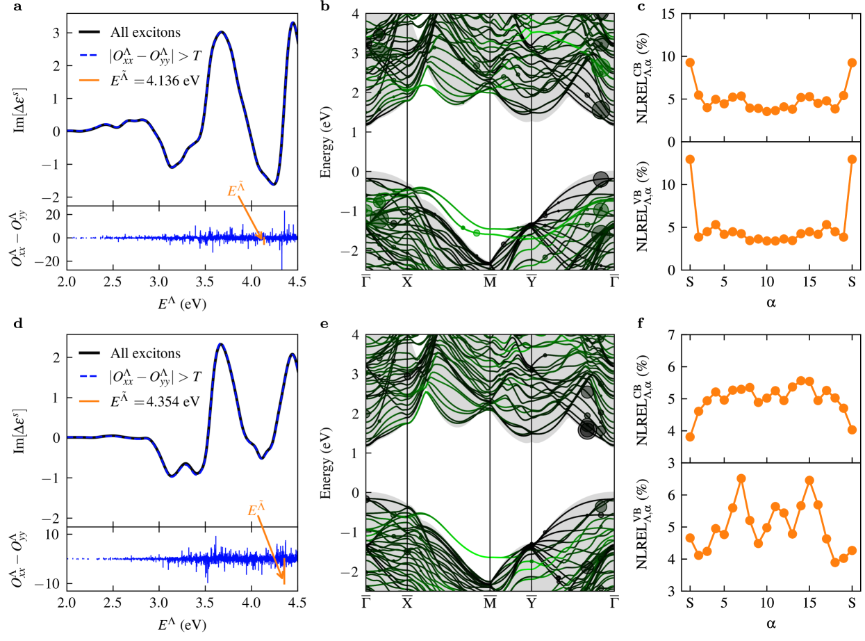
As demonstrated by our toy model in the introduction, analysis of RA spectra alone provides limited insight into the origin of RAS features, especially SIBA features, as BESA effects may shroud their origin (cf. Fig. 1). To address this, we focus directly on the surface dielectric anisotropy . To simplify the analysis, we consider only excitons that contribute strongly to the RAS, defined as those with , where is a threshold set to the average contribution of all excitons within the RAS energy range (see Supplementary Note 3 for details). Even with this constraint, approximately excitons remain for analysis for each surface reconstruction. In the upper panels of Fig. 3a and d, we show the surface dielectric anisotropy for both reconstructions, demonstrating that our exciton subset already accurately reproduces the surface dielectric anisotropy. Furthermore, the lower panels of Fig. 3a and d show that individual excitons do not dominate the contributions to each RAS feature. Instead, each feature results from a complex summation of positive and negative contributions, with the dominant contribution emerging only when all excitons are considered together. Note that the imaginary part of the surface dielectric anisotropies already looks remarkably similar to the RA spectra shown in Fig. 2d and h, with negative anisotropies at and . Therefore, we conclude that the SIBA features seen in the RAS in Fig. 2d and h are not only caused by the BESA effect visible in the model system (cf. Fig. 1). To investigate the origin of these features in the imaginary part of the surface dielectric function, we now focus on a detailed analysis of the contributing excitons.
First, we illustrate how a conventional fatband analysis and our NLREL measure can be used to analyze the origin of individual excitons. To do this, we selected one exciton for each surface reconstruction, highlighted in orange in the bottom panels of Fig. 3a and d. Figures 3b and 3e show the corresponding surface band structures, with the projection onto the surface layer highlighted in green (cf. Fig. 2d and g). We have added circles to the surface band structures for all transitions contributing to the oscillator strength, whose size is proportional to , while their color indicates the projection: black circles correspond to bulk states, and green circles represent states localized on surface atoms. The NLREL values for the selected excitons are shown in Fig. 3c and f.
For the Si(100):As reconstruction (Fig. 3 top row) we have chosen an exciton with a strong contribution from surface states. The fatband representation of the surface band structure shown in Fig. 3b, highlights the localization of this particular exciton at surface states throughout the whole surface Brillouin zone (green circles), with some contributions from bulk states between to and (black circles). This observation is directly supported by the NLREL plot in Fig. 3c. The VB and CB contributions are localized directly at the surface, while all other layers contribute uniformly.
For the Si(100):As-Si-H reconstruction (Fig. 3 bottom row) we have chosen an exciton with strong bulk contributions. The fatband representation of the surface band structure in Fig. 3e shows much more pronounced bulk transitions between the and points, visible as black circles. Again, the NLREL in Fig. 3f reflects this, showing that the exciton is more localized in the center of the slab compared to the surface layer, with layer contributions increasing as one goes deeper into the slab. Here one should not be surprised that the NLREL in Fig. 4f is not symmetric around the center of the slab, since the slab has only a center of inversion and not perfect mirror symmetry around the middle layer.
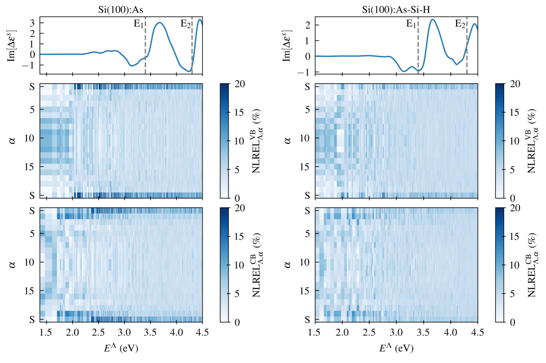
In summary, one could use the presented fatband analysis in conjunction with our NLREL to study the localization of individual excitons. However, this is impractical for the subset of excitons that all contribute to the RAS in some non-trivial way (see the lower panels of Fig. 3a and 3d), so we resort to the NLREL maps shown in Fig. 4, which streamline the analysis considerably.
However, before discussing the actual NLREL maps shown in Fig. 4, it is worth contemplating what one would expect these maps to look like, especially around the SIBA features at and . Recalling the quote about the origin of the SIBA features, i.e., ”bulk-like electronic states perturbed by the surface” from Ref. [29] and the conclusion drawn from Ref. [7]: ”It is shown that excitonic effects via strong modifications of the optical response of surface-modified bulk wave functions determine largely the line shape of the optical features.”, we would expect the following: Features in the surface dielectric anisotropy shown in Fig. 3a and d at and would be localized in layers deeper in the slab toward the ’bulk’ region, caused by perturbations of the bulk wave function by the surface reconstructions. Other features may originate directly from the surface, i.e., the NLREL map would show strong localization at or just below the surface.
Looking at the NLREL maps in Fig. 4, our expectations are not met. In the Si(100):As surface reconstruction, almost all of the excitons above eV are localized at the surface. The few excitons below eV are localized in the ’bulk’ region of the slab, while having almost no anisotropy, as can be seen by looking at the surface dielectric anisotropy in the upper panel of the left column of Fig. 4. The VB and CB contribution looks similar. For Si(100):As-Si-H, the VB states of the excitons below eV are similar to those of the Si(100):As reconstruction. However, the CB states are localized in the first layer below the surface. Again, these excitons have a vanishing contribution from the surface dielectric anisotropy. When comparing the NLREL maps for both surfaces above eV, differences become apparent, especially when comparing the CB states of the excitons. In the Si(100):As-Si-H surface reconstruction, the contribution of all layers to the excitons is averaged, and no strong surface or bulk localization is visible. However, the VB states are more localized at the surface, while all other layers have a small and similar contribution, similar to Si(100):As. After comparing the NLREL maps of both surfaces, it is clear that the excitons of the symmetric dimer motif of the Si(100):As reconstruction are much more localized at the surface compared to the asymmetric Si(100):As-Si-H reconstruction, yet their surface dielectric anisotropies are remarkably similar. In both systems we also find that the surface contribution tends to weaken slightly as one goes to higher energies, approaching the peak.
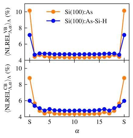
Now that we have discussed the NLREL maps and highlighted their differences, we question the term ’SIBA’ commonly used to label features that coincide with the critical energies of the bulk dielectric function, since strong bulk contributions are missing from both ’SIBA’ features in the NLREL maps, at least for Si(100):As. One could argue, however, that in the case of the Si(100):As-Si-H reconstruction, the features in the surface dielectric anisotropy around and may still be labeled ’SIBA’ because many bulk-like states from many layers in the slab contribute to the surface dielectric anisotropy. No clear surface localization is visible, yet no clear localization of excitons in the ’bulk’ region of the slab is visible either, as would be expected, similar to the VB states of the excitons below eV. The previously proposed picture of ”bulk-like electronic states perturbed by the surface” [29] may still be correct, but in the broader sense that all states, independent of the layer, are perturbed by the surface. Looking at the Si(100):As surface, the general labeling of features that coincide with the critical energies of the bulk dielectric function as ’SIBA’ breaks down completely because most of the excitons contributing to the surface dielectric anisotropy are localized at the surface. Both of the above observations become even clearer when looking at the energy averaged NLREL in Fig. 5. Here the difference between the surface contributions for the Si(100):As-Si-H and all other layers is small. For the Si(100):As the difference is significant.
As a side note, it would be interesting to know how these NLREL maps would look if the layer size were increased drastically. At the moment we are computationally limited in this regard, but we have checked NLREL maps with 10 layers using the same calculation parameters and observed very similar results.
II.3 Deciphering optical anisotropy of Si(100):V surfaces
Having shown that the NLREL maps can be used to identify the spatial origin of features in surface dielectric anisotropies, and that the origin of ’SIBA’ features is strongly system dependent, the physical effects behind them remain elusive. In particular, the cause of the strong surface localization of excitons above eV in the Si(100):As deserves further investigation. To gain insight into the mechanism behind this localization, we performed further calculations on Si(100)-:V surface reconstructions with symmetric dimers. Specifically, we repeated all the calculations presented for six additional systems. For three of them, we kept the Si(100):As geometry and replaced the As atoms with other group V atoms, i.e., P, Sb, and Bi. We will refer to these systems as Si(100):V@As (V = P, Sb, Bi) and again omit the from the surface reconstruction notation. The pseudopotentials for all group V atoms have the same valence electron configuration and differ only in the treatment of their core electrons and atomic size. The other three systems also follow the motif of a Si(100) surface reconstruction with a symmetric dimer group V-dimer in a supercell, but this time we have relaxed their geometry and will refer to them as Si(100):V. The calculations for six additional surfaces are performed with the same parameters as the previous ones for consistency, see Methods.
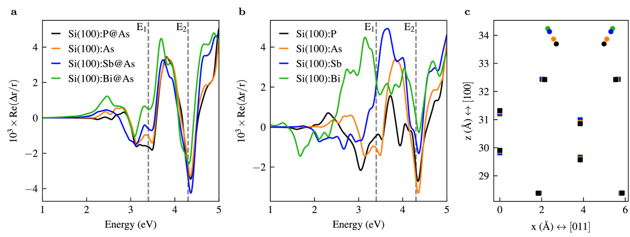
First, we comment on the Si(100):V@As surfaces calculated with a fixed Si(100):As geometry. Looking at their RA spectra in Fig. 6a, we observe that they all look remarkably similar, and interestingly, the anisotropies follow the order of the electronegativities of the group V elements, suggesting at least a small contribution of electric-field-induced anisotropy to the RAS [31, 30]. The associated surface band structures, the surface-projected density of states, and the NLREL maps shown in Supplementary Note 4 are also quite similar. In particular, the surface band structures show a strong similarity, with some differences in the gap between the two surface states propagating the bulk band gap close to the valence bands between the and points. This may be explained by the following simple argument: The geometry of the Sb and Bi dimers is drastically compressed (cf. Fig. 6c), leading to an increase in the ’band gap’ of their associated surface states, similar to the expected increase in band gap when a solid is compressed. This causes the surface states to look similar to those of an As dimer. In the case of the P dimer, the inverse argument may be applied.
Looking at the RA spectra in Fig. 6b for the relaxed Si(100):V geometries shown in Fig. 6c, we observe a strong change in the spectra below the feature. This is in line with the model calculations shown in Fig. 1: Now that the dimers are relaxed (decrease in P-P bond distance, increase in Sb-Sb and Bi-Bi bond distances, cf. Fig. 6c), the ’band gap’ between the associated surface states shrinks. Indeed, as shown in Supplementary Note 4, the surface bands shift toward the bulk band gap throughout the 2D Brillouin zone. This changes the transition space and thus the excitonic structure, which can be observed as features at lower energies in the RA spectra around and below . This enhanced contribution of surface states to the RA spectra and surface dielectric anisotropy is further highlighted by the corresponding NLREL maps in Supplementary Note 4.
Comparing the RAS (and additional illustrations in Supplementary Note 4) of the constraint and relaxed Si(100):V surfaces reveals the following: (i) Surface geometry is clearly the most dominant influence on RA spectra as it affects all parts of the electronic and derived optical properties. This even concerns the localization of the excitons that contribute most to the optical anisotropies. (ii) The feature in the RA spectrum of Si(100):As is coincidentally at the energy of bulk silicon and has nothing to do with ’SIBA’, i.e., ”bulk-like electronic states perturbed by the surface” [29], as it originates from surface states. This is further emphasized by the fact that the shape and position of this feature changes drastically in all other relaxed Si(100):V surfaces. (iii) The feature is clearly visible as a pronounced peak in all RA spectra (and surface dielectric anisotropies, see Supplementary Note 4). We therefore argue that this feature is a mixture of some surface contributions causing intensity changes and contributions from deeper layers, since surface contributions tend to weaken at higher energies around in all NLREL maps (see Supplementary Note 4). In addition, the BESA effect highlighted in the simple model system, cf. Fig. 1 and associated text, also contributes to the presence of the feature in all systems.
III Discussion
Our results provide new insight into the long-standing debate on the origin of bulk-related anisotropies in surface optical spectra. Traditionally, such features have been attributed to SIBA, i.e., ”bulk-like electronic states perturbed by the surface” [29].
First, we use a simple model system to show that these apparent ’SIBA’ features may arise from what we call bulk-enhanced surface anisotropy (BESA). Obviously, a closer examination of the dielectric anisotropy is needed to gain thorough insight into the origin of these features. Diving deeper, we perform an ab initio analysis of the excitonic contributions to the surface dielectric anisotropy of the technologically relevant arsenic-terminated Si(100) surface reconstruction utilizing the framework of MBPT. We introduce the LREL measure, which allows us to obtain a layer-resolved map of exciton origins, thereby disentangling the contributions of surface and subsurface states to the RA spectra. Again, our findings challenge the simple SIBA picture, as excitonic contributions to ’bulk-related’ features in RA spectra can be of different origins. For example, in the Si(100):As system, most excitons contributing to the optical anisotropy are localized directly at the surface, whereas they are rather delocalized for Si(100):As-Si-H. In the latter case, one could indeed speak of a SIBA effect. The comparison of NLREL results for constraint and relaxed Si(001):V surfaces shows that the surface localization of anisotropy-related excitons, in fact, depends sensitively on the structural details of the surface.
We identify three possible origins of RAS features that were previously attributed to SIBA: (i) BESA effects, where the bulk dielectric function strongly modulates the optical anisotropy, as illustrated in Fig. 1; (ii) features from surface states that coincidentally appear at bulk energies, as clearly seen in the Si(100):As reconstruction; and (iii) SIBA effects in the true sense of the word, as observed, e.g., for Si(100):As-Si-H. The present findings thus underline that a general classification of optical anisotropies at bulk critical points energies as SIBA does not take into account the complex origin of surface optical spectra. Rather, a detailed exciton-resolved analysis is indispensable for a proper understanding of the spectra.
The generality and simplicity of our LREL method makes it readily applicable to other semiconductor surfaces and heterostructures. By directly quantifying the contributions from individual atomic layers, our approach allows to disentangles the relative roles of surface and subsurface states in optical spectra and provides a quantitative framework that can be used to reexamine anisotropy features in previously studied systems.
In summary, the present work shows that ’bulk-related’ anisotropies in surface optical spectra do not necessarily originate from the bulk, but may as well be bulk-enhanced surface anisotropies, challenging the conventional SIBA interpretation. By introducing a versatile, general methodology for analyzing exciton localization, our work paves the way for a refined interpretation of surface optical responses that fully accounts for the complex interplay between surface chemistry, excitonic effects, and bulk contributions. We anticipate that these findings will spur further experimental and theoretical efforts to unravel the intricacies of surface optical phenomena.
IV Methods
Ab initio calculations
DFT and MBPT calculations were performed with a modified version of the version of VASP 5.4.4 [68, 69], which uses a plane-wave basis and the projector augmented-wave method [70]. Details about the code modification can be found in Supplementary Note 3. All key calculation parameters (plane-wave cutoff, k-point grid, vacuum size, and slab thickness) were systematically converged so that the ground state energy—and the surface energy for vacuum size and slab thickness—varied by less than meV. A plane-wave cutoff of eV and the PBEsol functional [74, 75] were used for all calculations unless otherwise noted. PBEsol was chosen, in particular to obtain accurate bulk and surface geometries. For all systems, the lattice constant was set to the value calculated with PBEsol, i.e., the Si bulk lattice constant of Å. The surfaces were modeled as non-vicinal, 20-layer slabs [25] with a center of inversion separated by a 16 Å vacuum and relaxed until the norms of all forces were smaller than eV/Å. Unless otherwise noted, surface calculations used a -centered k-point grid, while bulk calculations used a grid. Due to the high computational cost of GW calculations for surfaces, including the associated calculations needed to find converged parameters [76] and the necessary treatment of long-range screening [77], we resorted to the HSE06 functional [78, 79] to obtain a good approximation of the quasiparticle band structure for our relaxed slab models. Starting from the HSE06 results, we solved the BSE [38] within the Tamm-Dancoff approximation [67] using an analytical model for static screening [80] to obtain the surface dielectric tensor and the bulk dielectric function . Details and parameters for the static screening model are given in Supplementary Note 5. The broadening parameter from Eq. (4) has been set to eV. The BSE Hamiltonian for the surfaces included occupied and unoccupied Kohn-Sham orbitals. For the bulk, we included occupied and unoccupied Kohn-Sham orbitals on a dense -centered k-point grid. In all BSE calculations we have removed from the basis set valence and conduction band pairs whose difference in independent particle energy is greater than eV (OMEGAMAX=10). The orbital- and site-projected partial wavefunction characters , i.e., , were calculated with VASP input tags LORBIT=11 and RWIGS=-1, i.e., the values set in the PAW pseudopotentials were used as projection radii. The convergence of the BSE results with respect to the k-point grid is discussed in the main text.
IV.1 Sample preparation and measurements
We used -doped Si(100) substrates with a offcut angle towards the direction to prepare an A-type [54] Si(100)-:As-Si-H surface, analogous to Ref. [61]. Here we want to emphasize that the difference between and affects the orientation of the dimers along or perpendicular to the step edges of a vicinal surface, and therefore this is only an ”experimental” detail. This difference is well illustrated in Fig. 1 of Ref. [54]. However, throughout the rest of the paper, we always refer to a reconstruction, since all ab initio calculations have been performed for non-vicinal surfaces, making this distinction irrelevant. The samples were prepared using an H2-based horizontal AIX-200 MOCVD reactor (Aixtron). The entire MOCVD process was monitored in situ by RAS (LayTec EpiRAS-200). The Si(100) substrates here were first deoxidized by annealing under constant hydrogen flow for min at and mbar in MOCVD. Subsequently, the surface was prepared by exposure to tertiarybutylarsine (TBAs) at and 950 mbar. Here, a sequence of opening and closing the TBAs source was applied while maintaining a constant hydrogen flow [54]. This stepwise exposure increases the surface order, and exposure to TBAs prepares double layer steps on the surface, resulting in more pronounced RAS peak amplitudes. After exposure, the samples were cooled under constant hydrogen flow and RA spectra were recorded at K as shown in Supplement Note 6.
After preparation, the samples were first transferred to a cryostat (Montana Instruments Cryostation) using an MOCVD-to-UHV shuttle to prevent surface contamination [81]. Here, the custom copper cryostat head was first cooled by a closed-loop helium setup that reduced the pressure inside the cryostat from HV to UHV as it cooled. The sample, mounted on a molybdenum carrier, was then inserted into the copper cooling head while a series of LT RA spectra were acquired at a sample temperature of approximately K. Details regarding sample temperature estimation are given in Supplement Note 6. Following the LT RAS measurements, the sample was further transferred to LEED (specs ErLEED 100), XPS (monochromated Al-K, specs Focus 500/Phoibos 150/1D-DLD-43-100) to ensure that no contamination had occurred during sample transfer or in the cryostat that would cause structural or chemical changes, see Supplementary Note 7.
V Data and Code Availability
The data generated and the post-processing code used in this study are available from the corresponding author upon reasonable request.
VI Acknowledgments
We thank the staff of the Compute Center of the Technische Universität Ilmenau and especially Mr. Henning Schwanbeck for providing an excellent research environment. M.G. would like to thank Malte Grunert for asking thought-provoking questions, providing constructive feedback as a proofreader, and contributing to a delightful and productive office atmosphere. This work is supported by the Carl Zeiss Stiftung (funding code: P2023-02-008), the German Federal Ministry of Education and Research (BMBF, proj. H2Demo, proj. no. 03SF0619I), and the DFG (TRR 142/3-2025 proj. no. 231447078). We acknowledge the Paderborn Center for Parallel Computing (PC2) for grants of high-performance computer time.
VII Competing interests
The authors declare no competing interests.
Author contributions
M.G. conceived the idea, carried out the calculations, analyzed the data, visualized all results, and wrote the first draft of the manuscript. E.R. suggested the model calculations. K.D.H. prepared the samples, performed the LEED, XPS, and LT RAS measurements and evaluated the experimental results. C.Y.B. assisted the sample preparation and evaluation of experimental results. A.P. advised the experimental planning. M.G., W.G.S., and E.R. discussed and interpreted the theoretical results. T.H., W.G.S., and E.R. supervised the work; all authors revised and approved the manuscript.
References
- Aspnes and Studna [1985] D. E. Aspnes and A. A. Studna, Anisotropies in the Above—Band-Gap Optical Spectra of Cubic Semiconductors, Phys. Rev. Lett. 54, 1956–1959 (1985).
- Mochán and Barrera [1985] W. L. Mochán and R. G. Barrera, Intrinsic surface-induced optical anisotropies of cubic crystals: Local-field effect, Phys. Rev. Lett. 55, 1192–1195 (1985).
- Kipp et al. [1996] L. Kipp, D. K. Biegelsen, J. E. Northrup, L.-E. Swartz, and R. D. Bringans, Reflectance difference spectroscopy: Experiment and theory for the model system Si(001):As and application to Si(001), Phys. Rev. Lett. 76, 2810–2813 (1996).
- Uwai and Kobayashi [1997] K. Uwai and N. Kobayashi, Surface termination effect on reflectance spectra of GaAs, Phys. Rev. Lett. 78, 959–962 (1997).
- Rohlfing and Louie [1999] M. Rohlfing and S. G. Louie, Excitons and optical spectrum of the Si Surface, Phys. Rev. Lett. 83, 856–859 (1999).
- Sheridan et al. [2000] B. Sheridan, D. S. Martin, J. R. Power, S. D. Barrett, C. I. Smith, C. A. Lucas, R. J. Nichols, and P. Weightman, Reflection Anisotropy Spectroscopy: A New Probe for the Solid-Liquid Interface, Phys. Rev. Lett. 85, 4618–4621 (2000).
- Hahn et al. [2001] P. H. Hahn, W. G. Schmidt, and F. Bechstedt, Bulk excitonic effects in surface optical spectra, Phys. Rev. Lett. 88, 016402 (2001).
- Chandola et al. [2009] S. Chandola, K. Hinrichs, M. Gensch, N. Esser, S. Wippermann, W. G. Schmidt, F. Bechstedt, K. Fleischer, and J. F. McGilp, Structure of Si(111)-In nanowires determined from the midinfrared optical response, Phys. Rev. Lett. 102, 226805 (2009).
- Kumar and Patterson [2017] P. Kumar and C. H. Patterson, Dielectric anisotropy of the GaP/Si interface from first-principles theory, Phys. Rev. Lett. 118, 237403 (2017).
- Kress et al. [1997] C. Kress, A. Shkrebtii, and R. Del Sole, Surface reflectance anisotropy of C(100) and Si(100) ab initio calculations within the pseudopotential plane wave approach, Surf. Sci. 377–379, 398–403 (1997).
- Schmidt et al. [2001] W. G. Schmidt, F. Bechstedt, and J. Bernholc, Terrace and step contributions to the optical anisotropy of Si(001) surfaces, Phys. Rev. B 63, 045322 (2001).
- Hogan et al. [2003] C. Hogan, R. Del Sole, and G. Onida, Optical properties of real surfaces from microscopic calculations of the dielectric function of finite atomic slabs, Phys. Rev. B 68, 035405 (2003).
- Fuchs et al. [2005] F. Fuchs, W. G. Schmidt, and F. Bechstedt, Understanding the optical anisotropy of oxidized Si(001) surfaces, Phys. Rev. B 72, 075353 (2005).
- Zorn et al. [1999] M. Zorn, P. Kurpas, A. I. Shkrebtii, B. Junno, A. Bhattacharya, K. Knorr, M. Weyers, L. Samuelson, J. T. Zettler, and W. Richter, Correlation of InGaP(001) surface structure during growth and bulk ordering, Phys. Rev. B 60, 8185–8190 (1999).
- Hahn et al. [2003] P. H. Hahn, W. G. Schmidt, F. Bechstedt, O. Pulci, and R. Del Sole, P-rich GaP surface: A hydrogen-adsorbate structure determined from first-principles calculations, Phys. Rev. B 68, 033311 (2003).
- Fazi et al. [2013] L. Fazi, C. Hogan, L. Persichetti, C. Goletti, M. Palummo, A. Sgarlata, and A. Balzarotti, Intermixing and buried interfacial structure in strained Ge/Si(105) facets, Phys. Rev. B 88, 195312 (2013).
- Hogan et al. [2018] C. Hogan, O. Pulci, P. Gori, F. Bechstedt, D. S. Martin, E. E. Barritt, A. Curcella, G. Prevot, and Y. Borensztein, Optical properties of silicene, Si/Ag(111), and Si/Ag(110), Phys. Rev. B 97, 195407 (2018).
- Palummo et al. [1999] M. Palummo, G. Onida, R. Del Sole, and B. S. Mendoza, Ab initio optical properties of Si(100), Phys. Rev. B 60, 2522–2527 (1999).
- Castillo et al. [2003] C. Castillo, B. S. Mendoza, W. G. Schmidt, P. H. Hahn, and F. Bechstedt, Layer-by-layer analysis of surface reflectance anisotropy in semiconductors, Phys. Rev. B 68, 041310 (2003).
- Schmidt et al. [2003] W. G. Schmidt, S. Glutsch, P. H. Hahn, and F. Bechstedt, Efficient method to solve the Bethe-Salpeter equation, Phys. Rev. B 67, 085307 (2003).
- Landmann et al. [2015] M. Landmann, E. Rauls, W. G. Schmidt, M. D. Neumann, E. Speiser, and N. Esser, GaN -plane: Atomic structure, surface bands, and optical response, Phys. Rev. B 91, 035302 (2015).
- Ruiz Alvarado et al. [2023] I. A. Ruiz Alvarado, M. A. Zare Pour, T. Hannappel, and W. G. Schmidt, Structural fingerprints in the reflectance anisotropy of AlInP(001), Phys. Rev. B 108, 045410 (2023).
- Palummo et al. [2009] M. Palummo, N. Witkowski, O. Pluchery, R. Del Sole, and Y. Borensztein, Reflectance-anisotropy spectroscopy and surface differential reflectance spectra at the Si(100) surface: Combined experimental and theoretical study, Phys. Rev. B 79, 035327 (2009).
- Hingerl et al. [2001] K. Hingerl, R. E. Balderas-Navarro, A. Bonanni, P. Tichopadek, and W. G. Schmidt, On the origin of resonance features in reflectance difference data of silicon, Applied Surface Science 175-176, 769–776 (2001).
- Sole and Onida [1999] R. D. Sole and G. Onida, Surface versus crystal-termination effects in the optical properties of surfaces, Phys. Rev. B 60, 5523–5528 (1999).
- Arciprete et al. [2003] F. Arciprete, C. Goletti, E. Placidi, P. Chiaradia, M. Fanfoni, F. Patella, C. Hogan, and A. Balzarotti, Surface versus bulk contributions from reflectance anisotropy and electron energy loss spectra of the surface, Phys. Rev. B 68, 125328 (2003).
- Hogan et al. [2004] C. Hogan, D. Paget, O. E. Tereshchenko, L. Reining, and G. Onida, Optical anisotropy induced by cesium adsorption on the as-rich reconstruction of GaAs(001), Phys. Rev. B 69, 125332 (2004).
- Hingerl et al. [2000] K. Hingerl, R. E. Balderas-Navarro, W. Hilber, A. Bonanni, and D. Stifter, Surface-stress-induced optical bulk anisotropy, Phys. Rev. B 62, 13048–13052 (2000).
- Schmidt et al. [2000] W. G. Schmidt, N. Esser, A. M. Frisch, P. Vogt, J. Bernholc, F. Bechstedt, M. Zorn, T. Hannappel, S. Visbeck, F. Willig, and W. Richter, Understanding reflectance anisotropy: Surface-state signatures and bulk-related features in the optical spectrum of InP, Phys. Rev. B 61, R16335–R16338 (2000).
- Schmidt et al. [2002] W. G. Schmidt, F. Bechstedt, W. Lu, and J. Bernholc, Interplay of surface reconstruction and surface electric fields in the optical anisotropy of GaAs(001), Phys. Rev. B 66, 085334 (2002).
- Acosta-Ortiz and Lastras-Martínez [1989] S. E. Acosta-Ortiz and A. Lastras-Martínez, Electro-optic effects in the optical anisotropies of (001) GaAs, Phys. Rev. B 40, 1426–1429 (1989).
- Schmidt et al. [2004] W. Schmidt, K. Seino, P. Hahn, F. Bechstedt, W. Lu, S. Wang, and J. Bernholc, Calculation of surface optical properties: from qualitative understanding to quantitative predictions, Thin Solid Films 455–456, 764–771 (2004).
- Weightman et al. [2005] P. Weightman, D. S. Martin, R. J. Cole, and T. Farrell, Reflection anisotropy spectroscopy, Rep. Prog. Phys. 68, 1251–1341 (2005).
- Aspnes et al. [1998] D. E. Aspnes, L. Mantese, K. A. Bell, and U. Rossow, Photon-induced localization and final-state correlation effects in optically absorbing materials, J. Vac. Sci. Technol. B 16, 2367–2372 (1998).
- Mantese et al. [1999a] L. Mantese, Q. K. Xue, T. Sakurai, and D. E. Aspnes, Analysis of high-index Si(001) surfaces by reflectance difference spectroscopy, J. Vac. Sci. Technol. A 17, 1652–1656 (1999a).
- Mantese et al. [1999b] L. Mantese, K. Bell, D. Aspnes, and U. Rossow, Photon-induced localization in optically absorbing materials, Phys. Lett. A 253, 93–97 (1999b).
- Rossow et al. [2000] U. Rossow, L. Mantese, and D. E. Aspnes, Surface-induced optical anisotropy of Si and Ge, J. Vac. Sci. Technol. B 18, 2229–2231 (2000).
- Onida et al. [2002] G. Onida, L. Reining, and A. Rubio, Electronic excitations: density-functional versus many-body Green’s-function approaches, Rev. Mod. Phys. 74, 601–659 (2002).
- Albrecht et al. [1998] S. Albrecht, L. Reining, R. Del Sole, and G. Onida, Ab initio calculation of excitonic effects in the optical spectra of semiconductors, Phys. Rev. Lett. 80, 4510–4513 (1998).
- Fuchs et al. [2008] F. Fuchs, C. Rödl, A. Schleife, and F. Bechstedt, Efficient approach to solve the Bethe-Salpeter equation for excitonic bound states, Phys. Rev. B 78, 085103 (2008).
- Gorelov et al. [2022] V. Gorelov, L. Reining, M. Feneberg, R. Goldhahn, A. Schleife, W. R. L. Lambrecht, and M. Gatti, Delocalization of dark and bright excitons in flat-band materials and the optical properties of V2O5, Npj Comput. Mater. 8, 94 (2022).
- Acharya et al. [2023] S. Acharya, D. Pashov, C. Weber, M. van Schilfgaarde, A. I. Lichtenstein, and M. I. Katsnelson, A theory for colors of strongly correlated electronic systems, Nat. Commun. 14, 5565 (2023).
- Varrassi et al. [2024] L. Varrassi, P. Liu, and C. Franchini, Quasiparticle and excitonic properties of monolayer SrTiO3, Phys. Rev. Mater. 8, 024001 (2024).
- Palummo et al. [2004] M. Palummo, O. Pulci, R. D. Sole, A. Marini, P. Hahn, W. G. Schmidt, and F. Bechstedt, The Bethe–Salpeter equation: a first-principles approach for calculating surface optical spectra, J. Phys. Condens. Matter 16, S4313–S4322 (2004).
- May et al. [2013] M. M. May, O. Supplie, C. Höhn, R. van de Krol, H.-J. Lewerenz, and T. Hannappel, The interface of GaP(100) and H2O studied by photoemission and reflection anisotropy spectroscopy, New J. Phys. 15, 103003 (2013).
- May et al. [2014] M. M. May, H.-J. Lewerenz, and T. Hannappel, Optical in Situ Study of InP(100) Surface Chemistry: Dissociative Adsorption of Water and Oxygen, J. Phys. Chem. C 118, 19032–19041 (2014).
- May and Sprik [2018] M. M. May and M. Sprik, Water adsorption on the P-rich GaP(100) surface: optical spectroscopy from first principles, New J. Phys. 20, 033031 (2018).
- Ostheimer et al. [2024] D. Ostheimer, C. Dreßler, M. Großmann, M. A. Zare Pour, S. Shekarabi, K. D. Hanke, J. Koch, A. Paszuk, E. Runge, and T. Hannappel, Water vapor interaction with well-ordered GaInP(100) surfaces, J. Phys. Chem. C 128, 19559–19569 (2024).
- Aspnes and Studna [1983] D. E. Aspnes and A. A. Studna, Dielectric functions and optical parameters of Si, Ge, GaP, GaAs, GaSb, InP, InAs, and InSb from 1.5 to 6.0 eV, Phys. Rev. B 27, 985–1009 (1983).
- Lautenschlager et al. [1987] P. Lautenschlager, M. Garriga, L. Vina, and M. Cardona, Temperature dependence of the dielectric function and interband critical points in silicon, Phys. Rev. B 36, 4821–4830 (1987).
- Supplie et al. [2017] O. Supplie, M. M. May, S. Brückner, N. Brezhneva, T. Hannappel, and E. V. Skorb, In situ characterization of interfaces relevant for efficient photoinduced reactions, Adv. Mater. Interfaces 4, 10.1002/admi.201601118 (2017).
- Supplie et al. [2018] O. Supplie, O. Romanyuk, C. Koppka, M. Steidl, A. Nägelein, A. Paszuk, L. Winterfeld, A. Dobrich, P. Kleinschmidt, E. Runge, and T. Hannappel, Metalorganic vapor phase epitaxy of III-V-on-silicon: Experiment and theory, Prog. Cryst. Growth Charact. Mater. 64, 103–132 (2018).
- Paszuk et al. [2018a] A. Paszuk, O. Supplie, B. Kim, S. Brückner, M. Nandy, A. Heinisch, P. Kleinschmidt, Y. Nakano, M. Sugiyama, and T. Hannappel, GaAsP/Si tandem solar cells: In situ study on GaP/Si:As virtual substrate preparation, Sol. Energy Mater. Sol. Cells 180, 343–349 (2018a).
- Paszuk et al. [2018b] A. Paszuk, O. Supplie, M. Nandy, S. Brückner, A. Dobrich, P. Kleinschmidt, B. Kim, Y. Nakano, M. Sugiyama, and T. Hannappel, Double-layer stepped Si(100) surfaces prepared in As-rich CVD ambience, Appl. Surf. Sci. 462, 1002–1007 (2018b).
- Nandy et al. [2021] M. Nandy, A. Paszuk, M. Feifel, C. Koppka, P. Kleinschmidt, F. Dimroth, and T. Hannappel, A route to obtaining low-defect III-V epilayers on Si(100) utilizing MOCVD, Cryst. Growth Des. 21, 5603–5613 (2021).
- May et al. [2017] M. M. May, D. Lackner, J. Ohlmann, F. Dimroth, R. van de Krol, T. Hannappel, and K. Schwarzburg, On the benchmarking of multi-junction photoelectrochemical fuel generating devices, Sustain. Energy Fuels 1, 492–503 (2017).
- Alqahtani et al. [2019] M. Alqahtani, S. Sathasivam, F. Cui, L. Steier, X. Xia, C. Blackman, E. Kim, H. Shin, M. Benamara, Y. I. Mazur, G. J. Salamo, I. P. Parkin, H. Liu, and J. Wu, Heteroepitaxy of GaP on silicon for efficient and cost-effective photoelectrochemical water splitting, J. Mater. Chem. A 7, 8550–8558 (2019).
- Feifel et al. [2021] M. Feifel, D. Lackner, J. Schön, J. Ohlmann, J. Benick, G. Siefer, F. Predan, M. Hermle, and F. Dimroth, Epitaxial GaInP/GaAs/Si triple–junction solar cell with 25.9% AM1.5g efficiency enabled by transparent metamorphic AlxGa1-xAsyP1-y step-graded buffer structures, Sol. RRL 5, 2000763 (2021).
- Hannappel et al. [2024] T. Hannappel, S. Shekarabi, W. Jaegermann, E. Runge, J. P. Hofmann, R. van de Krol, M. M. May, A. Paszuk, F. Hess, A. Bergmann, A. Bund, C. Cierpka, C. Dreßler, F. Dionigi, D. Friedrich, M. Favaro, S. Krischok, M. Kurniawan, K. Lüdge, Y. Lei, B. Roldán Cuenya, P. Schaaf, R. Schmidt‐Grund, W. G. Schmidt, P. Strasser, E. Unger, M. F. Vasquez Montoya, D. Wang, and H. Zhang, Integration of multijunction absorbers and catalysts for efficient solar‐driven artificial leaf structures: A physical and materials science perspective, Sol. RRL 8, 2301047 (2024).
- Uhrberg et al. [1986] R. I. G. Uhrberg, R. D. Bringans, R. Z. Bachrach, and J. E. Northrup, Symmetric arsenic dimers on the Si(100) surface, Phys. Rev. Lett. 56, 520–523 (1986).
- Bohlemann et al. [2024] C. Y. Bohlemann, A. Flötotto, A. Paszuk, M. Nandy, M. Großmann, O. Romanyuk, K. D. Hanke, A. Gieß, P. Kleinschmidt, E. Runge, and T. Hannappel, Surface structure of MOVPE-prepared As-modified Si(100) substrates, Appl. Surf. Sci. 675, 160879 (2024).
- Schmidt [2005] W. G. Schmidt, Calculation of reflectance anisotropy for semiconductor surface exploration, Phys. Stat. Solid. B 242, 2751–2764 (2005).
- del Sole [1981] R. del Sole, Microscopic theory of optical properties of crystal surfaces, Solid State Commun. 37, 537–540 (1981).
- Del Sole and Fiorino [1984] R. Del Sole and E. Fiorino, Macroscopic dielectric tensor at crystal surfaces, Phys. Rev. B 29, 4631–4645 (1984).
- Manghi et al. [1990] F. Manghi, R. Del Sole, A. Selloni, and E. Molinari, Anisotropy of surface optical properties from first-principles calculations, Phys. Rev. B 41, 9935–9946 (1990).
- Selci et al. [1987] S. Selci, F. Ciccacci, G. Chiarotti, P. Chiaradia, and A. Cricenti, Surface differential reflectivity spectroscopy of semiconductor surfaces, J. Vac. Sci. Technol. A 5, 327–332 (1987).
- Bechstedt [2014] F. Bechstedt, Many-body approach to electronic excitations: Concepts and applications, Springer Series in Solid-State Sciences (Springer, New York, 2014).
- Kresse and Furthmüller [1996] G. Kresse and J. Furthmüller, Efficient iterative schemes for ab initio total-energy calculations using a plane-wave basis set, Phys. Rev. B 54, 11169–11186 (1996).
- Kresse and Joubert [1999] G. Kresse and D. Joubert, From ultrasoft pseudopotentials to the projector augmented-wave method, Phys. Rev. B 59, 1758–1775 (1999).
- Blöchl [1994] P. E. Blöchl, Projector augmented-wave method, Phys. Rev. B 50, 17953–17979 (1994).
- Noffsinger et al. [2012] J. Noffsinger, E. Kioupakis, C. G. Van de Walle, S. G. Louie, and M. L. Cohen, Phonon-Assisted Optical Absorption in Silicon from First Principles, Phys. Rev. Lett. 108, 167402 (2012).
- Marini [2008] A. Marini, Ab Initio Finite-Temperature Excitons, Phys. Rev. Lett. 101, 106405 (2008).
- Albrecht et al. [1999] S. Albrecht, L. Reining, G. Onida, V. Olevano, and R. Del Sole, Albrecht et al. Reply:, Phys. Rev. Lett. 83, 3971–3971 (1999).
- Perdew et al. [2008] J. P. Perdew, A. Ruzsinszky, G. I. Csonka, O. A. Vydrov, G. E. Scuseria, L. A. Constantin, X. Zhou, and K. Burke, Restoring the density-gradient expansion for exchange in solids and surfaces, Phys. Rev. Lett. 100, 136406 (2008).
- Perdew et al. [2009] J. P. Perdew, A. Ruzsinszky, G. I. Csonka, O. A. Vydrov, G. E. Scuseria, L. A. Constantin, X. Zhou, and K. Burke, Erratum: Restoring the density-gradient expansion for exchange in solids and surfaces [Phys. Rev. Lett. 100, 136406 (2008)], Phys. Rev. Lett. 102, 039902 (2009).
- Großmann et al. [2024] M. Großmann, M. Grunert, and E. Runge, A robust, simple, and efficient convergence workflow for GW calculations, Npj Comput. Mater. 10, 135 (2024).
- Freysoldt et al. [2008] C. Freysoldt, P. Eggert, P. Rinke, A. Schindlmayr, and M. Scheffler, Screening in two dimensions: calculations for surfaces and thin films using the repeated-slab approach, Phys. Rev. B 77, 235428 (2008).
- Heyd et al. [2003] J. Heyd, G. E. Scuseria, and M. Ernzerhof, Hybrid functionals based on a screened Coulomb potential, J. Chem. Phys. 118, 8207–8215 (2003).
- Heyd et al. [2006] J. Heyd, G. E. Scuseria, and M. Ernzerhof, Erratum: “Hybrid functionals based on a screened Coulomb potential” [J. Chem. Phys. 118, 8207 (2003)], J. Chem. Phys. 124, 219906 (2006).
- Bechstedt et al. [1992] F. Bechstedt, R. Del Sole, G. Cappellini, and L. Reining, An efficient method for calculating quasiparticle energies in semiconductors, Solid State Commun. 84, 765–770 (1992).
- Hannappel et al. [2004] T. Hannappel, S. Visbeck, L. Töben, and F. Willig, Apparatus for investigating metalorganic chemical vapor deposition-grown semiconductors with ultrahigh-vacuum based techniques, Rev. Sci. Instrum. 75, 1297–1304 (2004).