Fabrication of Metal Air Bridges for Superconducting Circuits using Two-photon Lithography
Abstract
Extraneous high frequency chip modes parasitic to superconducting quantum circuits can result in decoherence when these modes are excited. To suppress these modes, superconducting air bridges (AB) are commonly used to electrically connect ground planes together when interrupted by transmission lines. Here, we demonstrate the use of two-photon photolithography to build a supporting 3D resist structure in conjunction with a lift-off process to create AB. The resulting aluminum AB, have a superconducting transition temperature K and exhibit good mechanical strength up to lengths of 100 m. A measurable amount of microwave loss is observed when 35 AB were placed over a high- Ta quarter-wave coplanar waveguide resonator.
Micro-fabricated superconducting circuits have emerged as a leading candidate for quantum computers. Arute et al. (2019); Kim et al. (2023) However, designing a chip with increased number of qubits requires careful consideration of signal routing and elimination of unwanted modes. Coplanar waveguides (CPW), which are used for transmission lines and resonators,Day et al. (2003); Pozar (2005) are one of the constituent parts of a planar superconducting circuit. When transmitting signals through a CPW, parasitic slotline modes can arise due to uneven voltages induced on either side of the ground planes separated by the center metal trace.Ponchak, Papapolymerou, and Tentzeris (2005) To suppress excitation of slotline modes, wire-bonds are one commonly used technique to electrically connect the ground planes together. Despite their easy installation, wire-bonds are proven to be ineffective shunts due to their millimeter lengths.Wenner et al. (2011) Instead, superconducting free-standing crossovers, or air bridges (AB), are more effective in suppressing the parasitic modes as well as providing a way of signal routing.Chen et al. (2014); Bu et al. (2025)
Various fabrication methods for AB have been explored and reported in the literature.Girgis, Liu, and Benkhedar (2006); Lankwarden et al. (2012); Abuwasib, Krantz, and Delsing (2013); Chen et al. (2014); Dunsworth et al. (2018); Jin et al. (2021); Janzen et al. (2022); Sun et al. (2022); Stavenga et al. (2023); Alegria et al. (2025); Bu et al. (2025) Typical methods for fabrication of AB often include multiple layers of resist, thermal reflow, and etching of excess metals, adding complexity and inconsistencies to the fabrication process. Furthermore, the dimensions and the mechanical strength of the bridge structures are often limited by the height of the resist, which is determined by the spin and reflow steps in the fabrication process.
Techniques towards building a 3D AB by using grayscale lithography or dielectric materials to form the supporting structure have been demonstrated in previous works,Girgis, Liu, and Benkhedar (2006); Dunsworth et al. (2018); Janzen et al. (2022); Sun et al. (2022); Stavenga et al. (2023) but a thermal reflow of the resist is constantly required to achieve a smooth surface. Here, we present a new method that exploits two-photon lithography (TPL) to fabricate aluminum air bridges (Al AB). TPL is a direct laser writing (DLW) method that utilizes non-linear two-photon processes of the resist.Maruo, Nakamura, and Kawata (1997) Fig. 1(a) illustrates the basic working principle of TPL. In a two-photon process, the extent of polymerization of the underlying resist depends on the laser intensity non-linearly. Goppert‐Mayer (1931); Kaiser and Garrett (1961) As a result, resists only polymerize in a confined volume near the focal point (FP) of the laser (voxel) where the light intensity exceeds the polymerization threshold. By moving the FP through the resist, three-dimensional lithography is performed. TPL has found applications in various fields, including micro-electromechanical systems, photonics, and biomedical engineering.Lei et al. (2020); van der Velden, Fan, and Staufer (2020); Harinarayana and Shin (2021) With its ability to create sub-micron scale 3D structures,Cao et al. (2013); Guney and Fedder (2016); van der Velden, Fan, and Staufer (2020) TPL potentially enables superconducting circuits with complexity not previously achievable using traditional two-dimensional fabrication techniques.
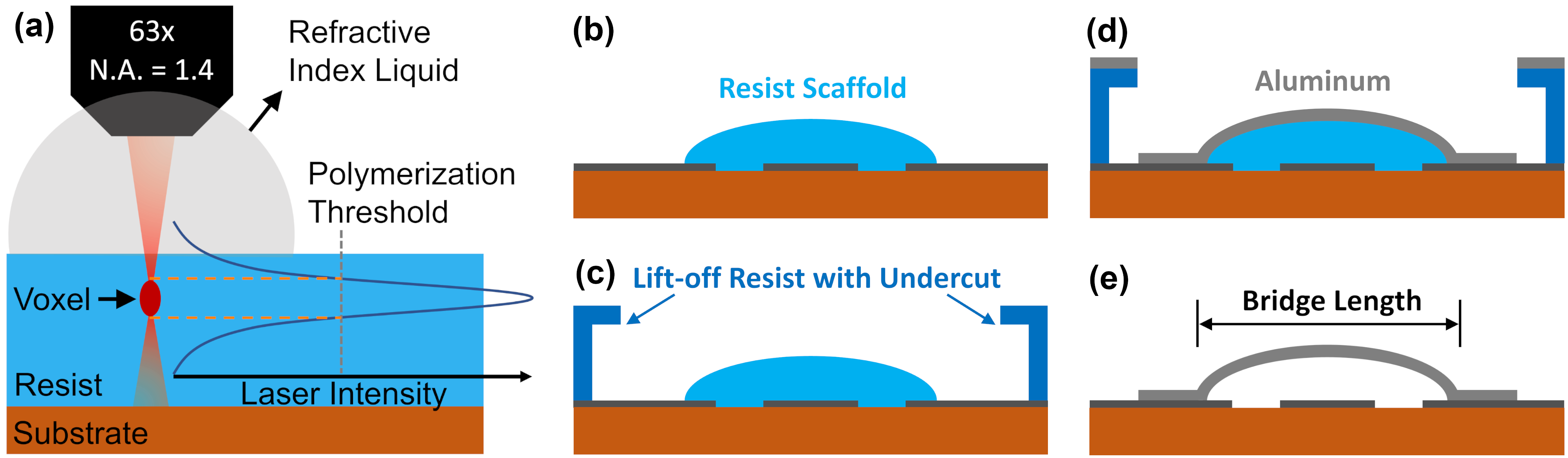
We start by presenting the key concepts of our fabrication process for Al AB in Fig. 1(b)-(e). First, a layer of negative-tone photoresist (AZ 15nXT) with a nominal thickness of 5.5 m was spun and baked on a device with patterned metal. The sacrificial scaffolds initially supporting the bridge structures were defined by exposing the resist using TPL (Photonic Professional GT2, Nanoscribe). The laser used, had a mean power of 50 mW, a wavelength of 780 nm, and illuminated the resist through an objective lens with a magnification of 63x and a numerical aperture of N.A. = 1.4. To obtain this N.A., the region between the objective and sample consisted of a matching refractive index liquid (Cargille) with = 1.6260 0.0002. After exposing and developing the solid resist scaffolds, a subsequent lift-off layer of 7 m photoresist (AZ nLOF 2070) was spun, baked, and exposed using a direct-write laser lithography tool (MLA150, Heidelberg). After developing this top layer of resist, which creates the aperture for the metal AB, the device was mounted in an electron beam evaporator (MEB550S, Plassys) for deposition of the metal AB. Prior to the deposition, an in situ aggressive argon ion mill was applied to remove the native oxide layer of the base metal and ensure good electrical contact. Then, 400 - 550 nm of Al was deposited at a rate of 0.5 nm/s to form the metal bridges. To remove the cross-linked resist formed during the argon ion mill step and assist the lift-off process, a reactive ion etch process using oxygen plasma was performed. Okuyama, Hashimoto, and Koguchi (1978); Chen et al. (2014) Finally, the two resists were dissolved and the AB were released by immersing the device in two subsequent baths of photoresist stripper (NI555, TechniStrip) at 80∘C.
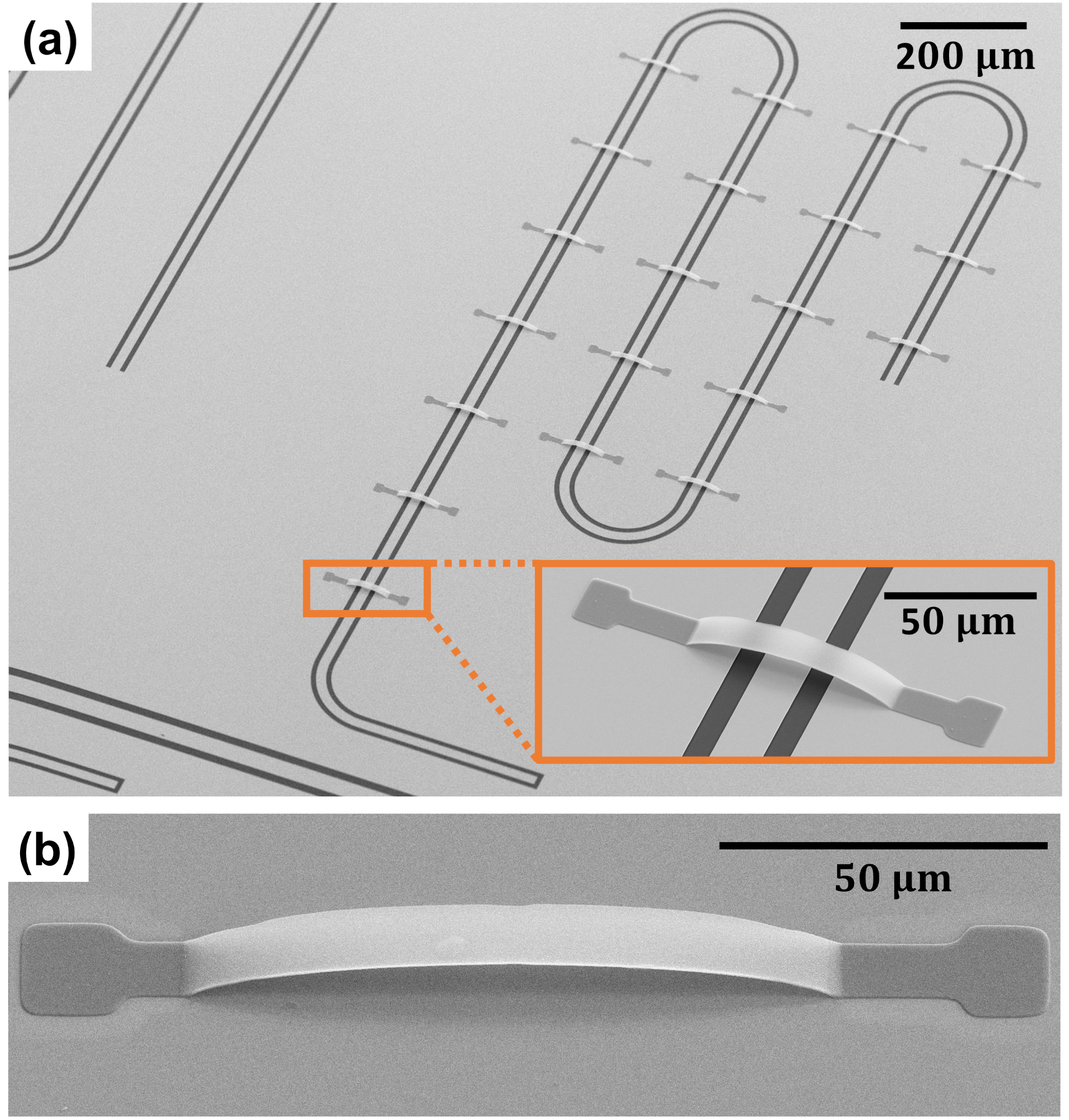
Using this TPL process, Al AB have been fabricated on both patterned reflective metal films on an optically transparent substrate such as sapphire and unpatterned substrates such as Si. Fig. 2 (a) shows a SEM micrograph of 20 AB, each AB has a length of 70 m and a width of 12 m creating a bridge for electrical ground signals, across a 6.15 GHz Ta quarter-wave CPW resonator. AB with lengths up to 100 m have been reliably fabricated (see Fig. 2 (b)).
To initially characterize the electrical properties of the resulting Al AB, 29 bridges in series were fabricated on a sapphire substrate and the resistance was measured using a four-probe measurement technique. The room temperature resistivity for the deposited Al AB was estimated to be , though we note that this estimate does not take into account the exact curved shape of the AB. The device was then cooled in a cryogen-free dilution refrigerator; a residual resistivity ratio of 3.85 and a sharp superconducting transition temperature of K were measured for the series of 29 Al AB.
The microwave loss, pertaining to the addition of our Al AB, was then characterized by fabricating three different numbers () of Al AB over Ta quarter-wave CPW resonators. For this work, a 200 nm thick tantalum film was deposited in a molecular-beam epitaxy system on a sapphire substrate. Four resonators coupled to a common transmission line were subsequently defined by photolithography and the Ta was etched using \ceCF4/\ceCHF3 in an inductively coupled plasma etcher. The CPW resonators nominally had a center trace of 16 m, gaps of 8 m, and different lengths such that the resonance frequencies () ranged from 5.38 to 6.15 GHz. We then fabricated 8, 20, and 35 AB, respectively, across three of the four resonators (see Fig. LABEL:FigS2(a) in the supplementary material for an optical image of the device).fno To measure the low-temperature microwave loss, the chip was then packaged and cooledfno ; Huang et al. (2023) in a cryogen-free dilution refrigerator with a base temperature of 10 mK. Using a vector network analyzer, the in-phase and out-of-phase S was measured as a function of frequency at different powers and temperatures. The internal quality factors, , were extracted by fitting S21 using the diameter correction method.fno ; Khalil et al. (2012)
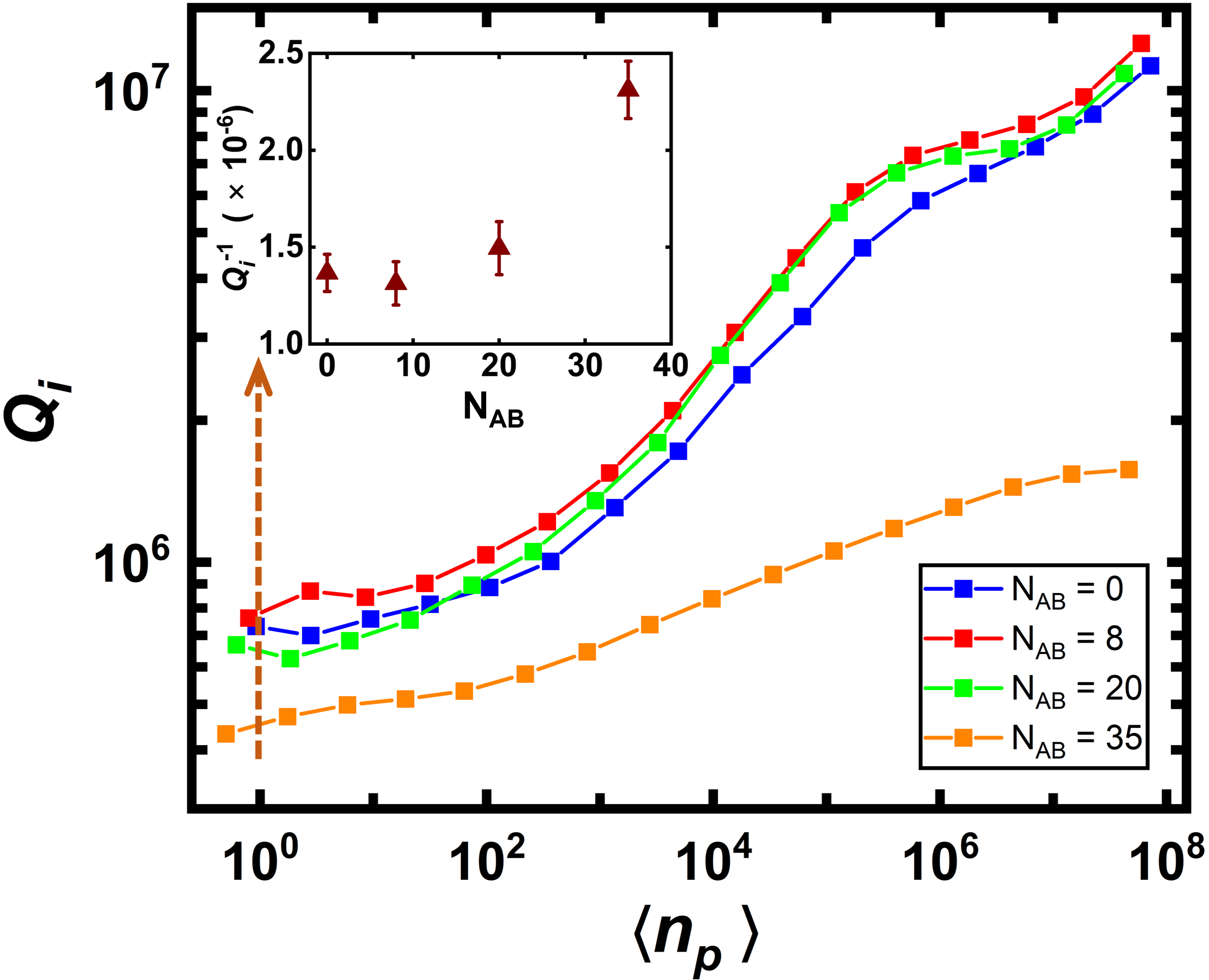
Fig. 3 shows the extracted as a function of the average stored photon number for the four different resonators at mK. At low powers corresponding to , the three resonators with = 0, 8, 20 had . These three resonators display a similar and weak increase of with increasing , reaching at stored powers corresponding to . On the other hand, the resonator device with = 35, displays more loss with at and at large powers. This observed loss for at is similar to the loss previously reported by other AB fabrication techniques (see inset Fig. 3). Chen et al. (2014); Dunsworth et al. (2018); Janzen et al. (2022) We note the dependence of on corresponding to the = 35 resonator can be well modeled as a power dependent loss similar to the other three resonators plus a power independent loss, .
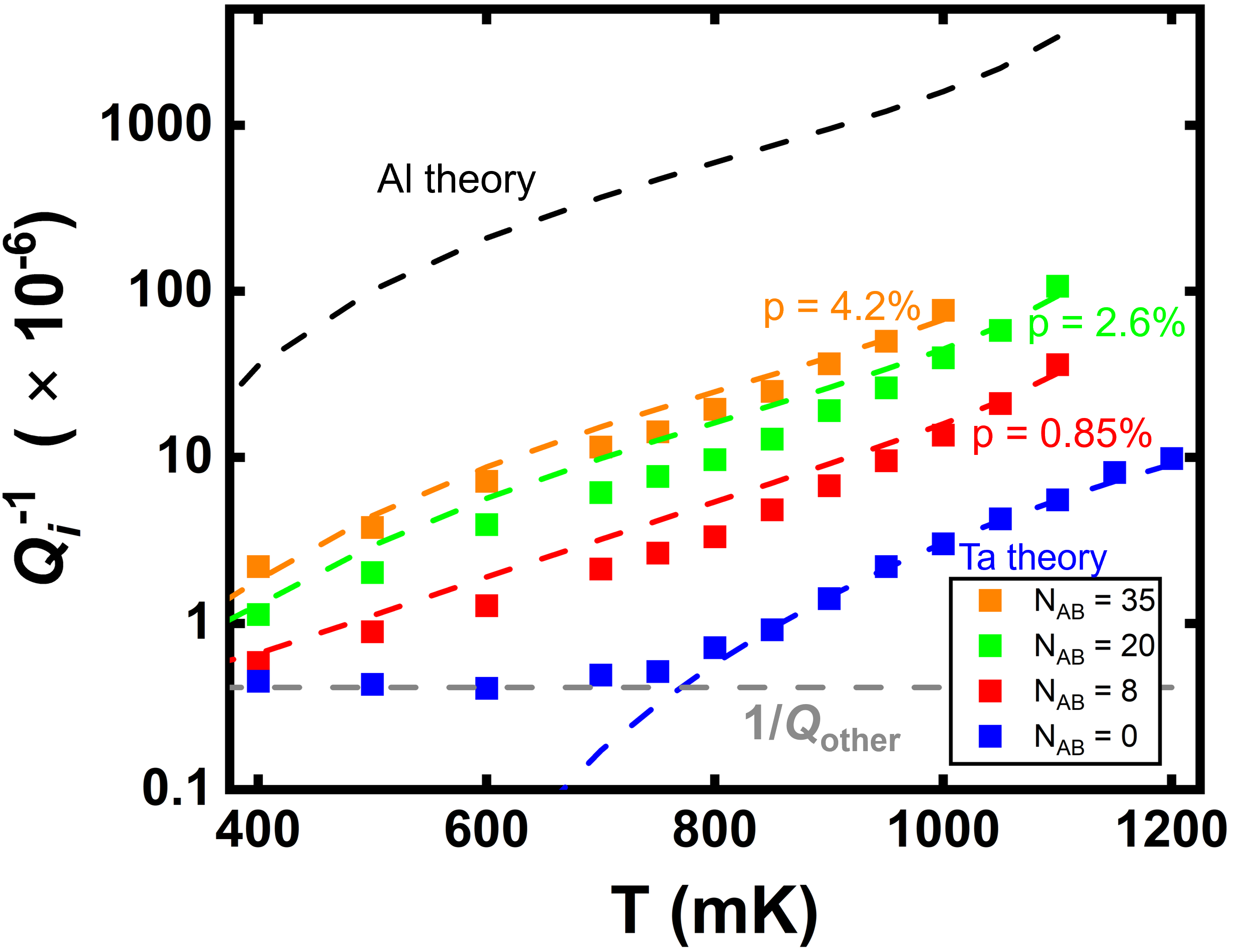
To determine if this source of loss is from inductive losses, we have determined the percentage of inductive energy stored in the AB for each . Since there is a significant difference in the superconducting gaps () between Al and Ta, the degradation of quality factors at elevated temperatures above 400 mK, depends on how much inductive energy is stored in the Al AB. Fig. 4 shows measurements of the loss () as a function of temperature from mK to above 1 K at . The exhibits a clear dependence on : with more air bridges added, the resonators display more loss at high temperatures. We model this dependence of on by assuming a percentage () of inductive energy stored in the Al AB and calculate the microwave loss of Al and Ta, respectively, as a function of temperature.
Using the theory of Mattis and Bardeen, Mattis and Bardeen (1958); Broom and Wolf (1977) associated with quasiparticles for a superconducting resonator with film thickness are given by
| (1) |
where is the fraction of kinetic to total (kinetic + geometric) inductance. The real and imaginary parts of the complex conductivity , and the London penetration depth as a function of are given by
| (2a) | ||||
| (2b) | ||||
| (2c) | ||||
Here, is the Fermi-Dirac distribution and is the normal state conductivity of the superconductor under consideration. By using , , , , 0.022, and 0.018, we theoretically calculate as a function of (see Fig.4) for Al (black dashed line) and Ta (blue dashed line). The percentage () of inductive energy stored in the AB is then extracted for each data set using
| (3) |
where is an unknown temperature independent loss. The fitted ’s range from 0.85% for up to 4.2 % for (see dashed lines in Fig.4). A similar but slightly reduced ’s were found when performing electromagnetic simulations using Ansys’ high frequency simulation software (HFSS).fno
By using these values, we can determine if the ’s measured at 10 mK are consistent with inductive losses. If we assume the power independent loss () observed in the resonator was inductive in nature and present in the resonator, the expected is
for , a value that is half of what is observed. This suggests that the observed loss with is not inductive in nature. Further tests including adjusting the placement of the AB and a larger sampling of would be needed to discern the loss mechanism.
In conclusion, we have used TPL and a lift-off process to create Al air bridges on superconducting CPW resonators, demonstrating a new technique for making AB. Our method can potentially be extended to create superconducting circuits with increased complexity enabled by the 3D capability of TPL. We confirmed the fabricated Al bridges to be superconducting and measured the loss when AB were placed over resonators. We have observed that with a measurable amount of loss is observed at 10 mK. Currently the loss mechanism is not consistent with being inductive in nature though further studies need to be conducted to fully understand the mechanism. Finally, the exposed TPL resist resolution perpendicular to the substrate is limited by the resist voxel size of 3 m.fno This limits our ability in creating an integrated lithographic process where the aperture at the top of the resist is defined in conjunction with the scaffold using TPL. Such an integrated process would be desired to further simplify the fabrication process.
Acknowledgements.
The authors thank Karen Grutter, Ryan Sochol, and Trisha Chakraborty for insightful discussions and suggestions.Data Availability
The data that support the findings of this study are available from the corresponding author upon reasonable request.
References
- Arute et al. (2019) F. Arute, K. Arya, R. Babbush, D. Bacon, J. C. Bardin, R. Barends, R. Biswas, S. Boixo, F. Brandao, D. A. Buell, B. Burkett, Y. Chen, Z. Chen, B. Chiaro, R. Collins, W. Courtney, A. Dunsworth, E. Farhi, B. Foxen, A. Fowler, C. Gidney, M. Giustina, R. Graff, K. Guerin, S. Habegger, M. P. Harrigan, M. J. Hartmann, A. Ho, M. Hoffmann, T. Huang, T. S. Humble, S. V. Isakov, E. Jeffrey, Z. Jiang, D. Kafri, K. Kechedzhi, J. Kelly, P. V. Klimov, S. Knysh, A. Korotkov, F. Kostritsa, D. Landhuis, M. Lindmark, E. Lucero, D. Lyakh, S. Mandra, J. R. McClean, M. McEwen, A. Megrant, X. Mi, K. Michielsen, M. Mohseni, J. Mutus, O. Naaman, M. Neeley, C. Neill, M. Y. Niu, E. Ostby, A. Petukhov, J. C. Platt, C. Quintana, E. G. Rieffel, P. Roushan, N. C. Rubin, D. Sank, K. J. Satzinger, V. Smelyanskiy, K. J. Sung, M. D. Trevithick, A. Vainsencher, B. Villalonga, T. White, Z. J. Yao, P. Yeh, A. Zalcman, H. Neven, and J. M. Martinis, Nature 574, 505–510 (2019).
- Kim et al. (2023) Y. Kim, A. Eddins, S. Anand, K. X. Wei, E. van den Berg, S. Rosenblatt, H. Nayfeh, Y. Wu, M. Zaletel, K. Temme, and A. Kandala, Nature 618, 500–505 (2023).
- Day et al. (2003) P. K. Day, H. G. LeDuc, B. A. Mazin, A. Vayonakis, and J. Zmuidzinas, Nature 425, 817–21 (2003).
- Pozar (2005) D. M. Pozar, Microwave Engineering, 3rd ed. (Wiley, 2005).
- Ponchak, Papapolymerou, and Tentzeris (2005) G. E. Ponchak, J. Papapolymerou, and M. M. Tentzeris, IEEE Trans. Microw. Theory Tech. 53, 713–717 (2005).
- Wenner et al. (2011) J. Wenner, M. Neeley, R. C. Bialczak, M. Lenander, E. Lucero, A. D. O’Connell, D. Sank, H. Wang, M. Weides, A. N. Cleland, and J. M. Martinis, Supercond. Sci. Technol. 24, 065001 (2011).
- Chen et al. (2014) Z. Chen, A. Megrant, J. Kelly, R. Barends, J. Bochmann, Y. Chen, B. Chiaro, A. Dunsworth, E. Jeffrey, J. Y. Mutus, P. J. J. O’Malley, C. Neill, P. Roushan, D. Sank, A. Vainsencher, J. Wenner, T. C. White, A. N. Cleland, and J. M. Martinis, Appl. Phys. Lett. 104, 052602 (2014).
- Bu et al. (2025) K. L. Bu, S. N. Huai, Z. X. Zhang, D. F. Li, Y. Li, J. J. Hu, X. P. Yang, M. C. Dai, T. Q. Cai, Y. C. Zheng, and S. Y. Zhang, npj Quantum Inf. 11, 17 (2025).
- Girgis, Liu, and Benkhedar (2006) E. Girgis, J. Liu, and M. L. Benkhedar, Appl. Phys. Lett. 88, 202103 (2006).
- Lankwarden et al. (2012) Y. J. Y. Lankwarden, A. Endo, J. J. A. Baselmans, and M. P. Bruijn, J. Low Temp. Phys. 167, 367–372 (2012).
- Abuwasib, Krantz, and Delsing (2013) M. Abuwasib, P. Krantz, and P. Delsing, J. Vac. Sci. Technol. B 31, 031601 (2013).
- Dunsworth et al. (2018) A. Dunsworth, R. Barends, Y. Chen, Z. Chen, B. Chiaro, A. Fowler, B. Foxen, E. Jeffrey, J. Kelly, P. V. Klimov, E. Lucero, J. Y. Mutus, M. Neeley, C. Neill, C. Quintana, P. Roushan, D. Sank, A. Vainsencher, J. Wenner, T. C. White, H. Neven, J. M. Martinis, and A. Megrant, Appl. Phys. Lett. 112, 063502 (2018).
- Jin et al. (2021) Y. Jin, M. Moreno, P. M. T. Vianez, W. K. Tan, J. P. Griffiths, I. Farrer, D. A. Ritchie, and C. J. B. Ford, Appl. Phys. Lett. 118, 162108 (2021).
- Janzen et al. (2022) N. Janzen, M. Kononenko, S. Ren, and A. Lupascu, Appl. Phys. Lett. 121, 094001 (2022).
- Sun et al. (2022) Y. T. Sun, J. Y. Ding, X. Y. Xia, X. H. Wang, J. W. Xu, S. Q. Song, D. Lan, J. Zhao, and Y. Yu, Appl. Phys. Lett. 121, 074001 (2022).
- Stavenga et al. (2023) T. Stavenga, S. A. Khan, Y. Liu, P. Krogstrup, and L. DiCarlo, Appl. Phys. Lett. 123, 024004 (2023).
- Alegria et al. (2025) L. D. Alegria, A. Abelson, E. Kim, S. Im, P. M. Voyles, V. Lordi, J. L. Dubois, and Y. J. Rosen, J. Appl. Phys. 137, 044402 (2025).
- Maruo, Nakamura, and Kawata (1997) S. Maruo, O. Nakamura, and S. Kawata, Opt. Lett. 22, 132–4 (1997).
- Goppert‐Mayer (1931) M. Goppert‐Mayer, Ann. Phys. 401, 273–294 (1931).
- Kaiser and Garrett (1961) W. Kaiser and C. G. B. Garrett, Phys. Rev. Lett. 7, 229–231 (1961).
- Lei et al. (2020) S. T. Lei, X. Zhao, X. M. Yu, A. M. Hu, S. Vukelic, M. B. G. Jun, H. E. Joe, Y. L. Yao, and Y. C. Shin, J. Manuf. Sci. Eng. Trans. ASME. 142, 031005 (2020).
- van der Velden, Fan, and Staufer (2020) G. van der Velden, D. Fan, and U. Staufer, Micro Nano Eng. 7, 100054 (2020).
- Harinarayana and Shin (2021) V. Harinarayana and Y. C. Shin, Opt. Laser Technol. 142, 107180 (2021).
- Cao et al. (2013) H. Z. Cao, M. L. Zheng, X. Z. Dong, F. Jin, Z. S. Zhao, and X. M. Duan, Appl. Phys. Lett. 102, 201108 (2013).
- Guney and Fedder (2016) M. G. Guney and G. K. Fedder, J. Micromech. Microeng. 26, 105011 (2016).
- Okuyama, Hashimoto, and Koguchi (1978) Y. Okuyama, T. Hashimoto, and T. Koguchi, J. Electrochem. Soc. 125, 1293–1298 (1978).
- (27) See supplementary material for device image, measurement setup, analysis method, and discussions on voxel size and electromagnetic simulations.
- Huang et al. (2023) Y. Z. Huang, Y. H. Huang, H. Z. Wang, Z. Steffen, J. Cripe, F. C. Wellstood, and B. S. Palmer, Appl. Phys. Lett. 123, 044001 (2023).
- Khalil et al. (2012) M. S. Khalil, M. J. A. Stoutimore, F. C. Wellstood, and K. D. Osborn, J. Appl. Phys. 111, 054510 (2012).
- Mattis and Bardeen (1958) D. C. Mattis and J. Bardeen, Phys. Rev. 111, 412–417 (1958).
- Broom and Wolf (1977) R. F. Broom and P. Wolf, Phys. Rev. B 16, 3100–3107 (1977).