- ACL
- atom-chip lattice
- SCL
- simple cubic lattice
- DRSC
- degenerate Raman sideband cooling
- PGC
- polarization gradient cooling
- TOF
- time-of-flight
- MOT
- magneto-optical trap
Atom-Chip Compatible Optical Lattice
Abstract
A lattice beam configuration which results in an isotropic 3D trap near the surface of an atom chip is described. The lattice is formed near the surface of a reflectively coated atom chip, where three incident beams and three reflected beams intersect. The coherent interference of these six beams form a phase-stable optical lattice which extends to the surface of the atom chip. The lattice is experimentally realized and the trap frequency is measured. Degenerate Raman sideband cooling is performed in the optical lattice, cooling 80 million atoms to .
1 Introduction
Magnetic and optical traps are powerful tools in atomic physics, and these two trap types have unique strengths and weaknesses. Magnetic traps offer greater flexibility to engineer potentials tailored to a specific application. Moreover, magnetic traps formed by an atom chip are well suited for use in portable and commercial devices due to their compact size, localized fields, low power consumption, and mature fabrication techniques. However magnetic traps only trap atoms in a low-field seeking Zeeman state, whereas optical traps are insensitive to the Zeeman state. Moreover, optical lattices commonly trap atoms in the Lamb-Dicke regime, which is required when performing sideband cooling.
To leverage the advantages of both technologies, an optical lattice must spatially overlap the trap created by an atom chip. Typically this requires an optical lattice to be formed within a few hundred micrometers of the atom chip. Two groups have reported trapping atoms in an optical lattice near an atom chip: Gallego et al. [1] were the first to combine an atom chip with a 1D optical lattice, while Straatsma et al. [2] extended this to a 3D optical lattice.
The lattice used by Straatsma et al. consisted of three, mutually orthogonal, retro-reflected beams. The light used to form the lattice had a short coherence length, such that each beam coherently interfered only with its retro-reflected counterpart. We will refer to this lattice design as the simple cubic lattice (SCL). With the SCL, two lattice beams must travel parallel to the atom chip. To achieve overlap with an atom chip magnetic trap, the chip-beam separation was . To minimize diffraction, incident lattice beams were displaced from the chip surface using periscoping optics bonded to the chip. The lattice beams used by Straatsma et al. were focused to a waist of .
In this work we present an alternative beam configuration which forms a 3D optical lattice near the surface of an atom chip. The lattice is formed by reflecting three incident beams off the surface of a reflectively coated atom chip. This design allows the lattice to be easily integrated into mirror magneto-optical trap (MOT) systems [3]. Because the lattice uses beams that are reflected from the atom chip, the design is not constrained by diffraction from the atom chip. Consequently, the lattice extends to within a wavelength of the atom chip. Furthermore, the lattice avoids the use of on-chip periscoping optics, thereby simplifying fabrication and improving optical access. Large beams may be used to create the lattice, which simplifies alignment and increases capture volume. Because the lattice forms at the surface of the atom chip, beam scatter from the chip may be imaged to further assist with beam alignment. We refer to this lattice as the atom-chip lattice (ACL).
In Sec. 2, we describe the beam geometry used to create the ACL. We present an expression for the lattice potential as well as formulas for the lattice properties. We compare the properties of the ACL to the SCL. We conclude this section with a brief discussion on the phase stability of the lattice. In Sec. 3, we describe an experimental implementation of the lattice. We present measurements of the lattice frequency, and demonstrate degenerate Raman sideband cooling (DRSC).
2 Atom Chip Lattice Theory
The far-off-resonant light that makes up an optical lattice interacts with the light induced dipole moment of an atom giving rise to the ac-Stark shift. The ac-Stark shift is given by
| (1) |
where the angled brackets denote a time-average, is the dynamic polarizability created through the interaction between the atom and light with angular frequency , is the electric field of the light, and denotes its complex-conjugate. In general, the electric field generated by incident plane waves is given by
| (2) |
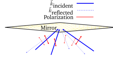
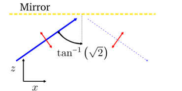
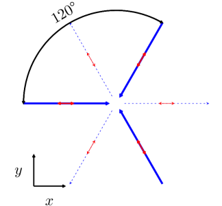
The ACL consists of three, coherent, red-detuned beams with equal intensity. All beams are directed towards a reflectively coated atom chip at an angle of incidence of . The beams are aligned to intersect at the surface of the atom chip. We define the z-axis as normal to the atom chip. Incident beams are separated by a in the xy-plane. In this configuration, incident beams are mutually orthogonal. All beams are linearly polarized with P-polarization. Fig. 1 illustrates the Poynting and polarization vectors for the beams used to create the ACL.
For the ACL, and are given as
The potential created by this lattice is
| (3) |
where and is the intensity of the beams used to create the lattice.
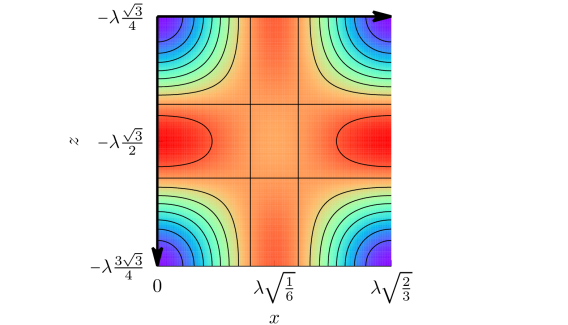
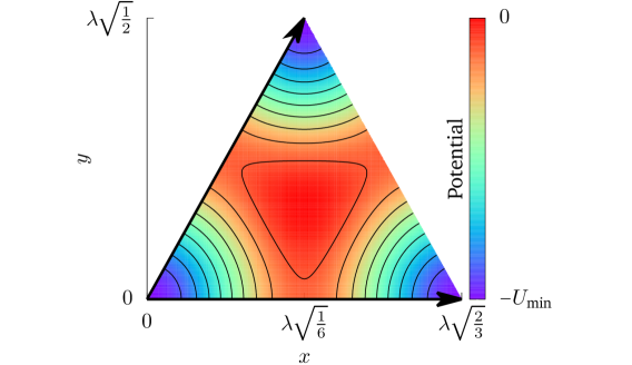
The resulting lattice has isotropic trap frequencies. There is translational symmetry along the z-axis with spatial periodicity of . In the xy-plane, local minima form equilateral triangles arranged in a hexagonal pattern. Minima are separated by in the xy-plane. The potential formed by the ACL is illustrated in Fig. 2 while the properties of the lattice are summarized in Tab. 1. The barrier described in Tab. 1 refers to the minimum potential barrier between adjacent lattice sites.
The properties of the ACL are independent of the phases of the incident beams as well as displacements in the reflecting mirror. A well-established rule[4] for lattice phase stability states that a lattice using coherently interfering beams to confine atoms in dimensions must have no more than independent phases. The ACL may appear to violate this rule, as the lattice is formed by the coherent interference of six beams. However, the ACL contains only four independent phases: three phases from the incident beams, with a fourth phase from the reflection from the surface. Because all three incident beams reflect off the same point of the same surface, all three beams receive a common phase shift upon reflection. Relative phase shifts in the incident beams result in a translation of the lattice in the xy-plane. Movement of the mirror results in a translation along the z-axis.
3 Experimental Realization
Experimental realization of the lattice was achieved using 87Rb. The system used for this experiment is similar to the one described in Ref. [5]. Atoms are prepared in a mirror MOT with the cloud center below the atom chip. Before loading into the optical lattice, the magnetic fields are ramped, moving the cloud below the atom chip. The atoms are further cooled to through polarization gradient cooling (PGC).
The lattice is formed using three beams from a 1:3 fiber splitter. Polarization-maintaining fibers are used to ensure the lattice beams maintain P-polarization. The beams are launched from fiber collimators mounted to custom pedestals angled to launch the beams with an angle of above the horizontal. The beams have beam waist and , , and of power. The lattice is tuned red of the resonance.
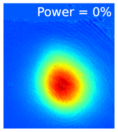
Alignment of the lattice is achieved with the help of an absorption imaging system with imaging axis oriented normal to the atom chip. The imaging beam is retro-reflected from the atom chip and directed into the imaging system via a beam splitting cube. The atoms are imaged following PGC. Lattice beams are aligned so that the center of the beams impinge on the atom chip at the location of the atoms following PGC. This is easily achieved through imaging the light scattered by the lattice beams off the surface of the atom chip.
We measure the fraction of atoms transferred from the MOT into the lattice using a horizontally oriented imaging system. The atoms are held in the lattice for then released for a time-of-flight (TOF). The resulting optical density, shown in Fig. 3, is fit to two Gaussians. From this analysis we calculate the fraction of atoms captured in the lattice. Using this technique we find that we transfer of the atoms from the MOT into the optical lattice.

The trap frequency of the lattice was measured using parametric heating. Heating was achieved by modulating the intensity of the lattice beams, while temperature was measured through TOF. The results of the parametric heating measurement show a trap frequency of , close to the expected frequency of .
The motional energy of atoms in the ACL is quantized such that the motional energy quanta are greater than the recoil energy transferred by near-resonant photon scatter; this regime is known as the Lamb-Dicke regime. Atoms in this limit are characterized by the Lamb-Dicke parameter, ; for the work presented here, . In the Lamb-Dicke regime, the probability that resonant photon scatter changes the motional energy of the atoms is reduced. This property of the Lamb-Dicke regime is exploited during the optical pumping stage of DRSC.
In DRSC, a small magnetic field is applied such that the Zeeman splitting between states equals the motional energy quantization created by the optical lattice. Off-resonant light drives the 2-photon degenerate Raman transitions between the and states, where is the quantum number describing the motional state of the trapped atom. This effectively enables the atoms to trade Zeeman energy for motional energy. Because this process is coherent, heating and cooling both occur with equal probability. Optical pumping is used to create a “ratchet,” allowing the atoms to repeatedly trade higher Zeeman energy for lower motional energy, while suppressing the reverse process.

In this experiment, our atoms are loaded into the ground state. As depicted in Fig. 4, optical pumping light is tuned to the resonance, while polarization and magnetic field direction are chosen so that the optical pumping photons are polarized with respect to the atoms. Because has only a single Zeeman state, , optical pumping photons only scatter when atoms are the highest Zeeman energy, lowest motional energy, state: . After scattering into these atoms decay back into the ground state where further cooling may occur. Because atoms are trapped in the Lamb-Dicke regime, any reduction in motional energy tends to be preserved during the optical pumping. This process is repeated until the atom is in both the lowest motional energy and lowest Zeeman energy state, . Atoms in this state are dark to both optical pumping and Raman light.
In preparation for DRSC, our atoms are cooled using PGC. Following this, the atoms are pumped into the state by tuning the MOT cooling light to the resonance, and tuning the MOT repump light red of the resonance; the atoms are pumped for . MOT and PGC light is extinguished, while the intensity of the optical lattice is ramped adiabatically over following the curve described in Ref. [6]. After loading into the lattice, the magnetic field is ramped over to create the Zeeman-motional degeneracy. Optical pumping and repump light is applied for . Following DRSC the optical lattice is extinguished and the magnetic field is zeroed. The temperature of the cloud is measured through TOF.
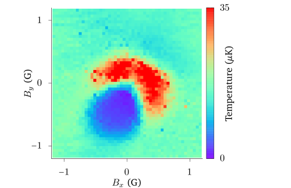
The magnetic field dependence of the DRSC was explored by performing a scan of the and magnetic bias fields. For each bias field, the temperature was calculated by measuring the cloud size following a and TOF. This data, shown in Fig. 5, shows clearly defined regions of Stokes heating and anti-Stokes cooling. The minimum temperature is seen at bias field of .
The best results were achieved by linearly ramping the intensity of the optical lattice light, as well as the magnetic fields and optical pumping detuning during the DRSC stage. The optimal experimental parameters were found using a particle swarm optimizer modified to handle stochastic data. The DRSC parameters were optimized to maximize phase-space density. In the optimal configuration, the optical lattice intensity starts fully on and ramps down to of max intensity. The magnetic field strength starts at and ramps down to . Lastly, the optical pumping is initially tuned blue of the resonance, and is increased to blue. Following optimization, we find that we cool 80 million atoms to horizontally and vertically.
4 Conclusions
We have presented an isotropic 3D optical lattice design which extends to the surface of an atom chip. The lattice does not require on-chip optics and may be formed using large beams, which enables increased capture volume while easing alignment requirements. Despite arising from the coherent interference of six beams, the optical lattice is phase stable due to the common phase shift applied to all three incident beams upon reflection. The lattice presented here represents a single example of a class of near-chip lattices which are formed by the reflection of lattice beams off the surface of an atom chip. Further lattice designs including anisotropic 3D lattices, 2D lattices, and blue-detuned lattices may be formed using this technique.
We experimentally demonstrated trapping of 87Rb in the ACL. We succeeded in transferring more than of the atoms from the MOT into this lattice. The frequency of the lattice was measured and found to be in close agreement with theory. We performed DRSC in the atom-chip lattice, cooling 80 million atoms to . The ability to perform DRSC near the atom chip could enable the rapid production of Bose-Einstein condensates and increase the measurement frequency of atom-wave interferometers.
Funding This work was funded by the Air Force Office of Scientific Research under lab task 22RVCOR017.
Disclosures The authors declare no conflicts of interest.
Disclaimer The views expressed are those of the authors and do not necessarily reflect the official policy or position of the Department of the Air Force, the Department of the Defense, or the U.S. Government.
References
- [1] D. Gallego, S. Hofferberth, T. Schumm, P. Krüger, and J. Schmiedmayer, \JournalTitleOpt. Lett. 34, 3463 (2009).
- [2] C. J. E. Straatsma, M. K. Ivory, J. Duggan, J. Ramirez-Serrano, D. Z. Anderson, and E. A. Salim, \JournalTitleOpt. Lett. 40, 3368 (2015).
- [3] J. Fortagh, A. Grossmann, C. Zimmermann, and T. W. Hänsch, \JournalTitlePhys. Rev. Lett. 81, 5310 (1998).
- [4] G. Grynberg, B. Lounis, P. Verkerk, J. Courtois, and C. Salomon, \JournalTitlePhys. Rev. Lett. 70, 2249 (1993).
- [5] M. B. Squires, S. E. Olson, B. Kasch, J. A. Stickney, C. J. Erickson, J. A. R. Crow, E. J. Carlson, and J. H. Burke, \JournalTitleApplied Physics Letters 109, 264101 (2016).
- [6] A. Kerman, “Raman sideband cooling and cold atomic collisions in optical lattices,” Doctoral dissertation, Stanford University (2002).