An integrated widely tunable linear isolator based on electro-optic Autler-Townes splitting
Abstract
Optical isolators are essential for laser protection and robust signal routing, but the incorporation of the necessary magneto-optic (MO) materials in foundries has remained a challenge. As an alternative, several integrated non-magnetic isolators based on acousto-optic (AO) and electro-optic (EO) spatio-temporal modulation have been proposed. Unlike MO isolators, these solutions are wavelength agnostic, though few published demonstrations reach performance that is comparable to MO devices. The most significant remaining concerns are on mitigating undesirable sidebands, lowering power consumption, achieving wide bandwidth or wide tunability, and having a design that is practical to deploy. Here we demonstrate a compact EO optical isolator, using thin film lithium niobate, that produces a very high isolation figure of merit ( dB contrast per dB of insertion loss) with THz-scale (8 nm) tunability and, due to its architecture, achieves linear operation with negligible sideband generation. The device uses a 20x smaller interaction length and consumes 64x less power compared to the state-of-the-art EO and AO architectures, without being subject to many of their technical constraints.
Magneto-optic isolators have persisted as the dominant non-reciprocal technology. However, there remain unsolved challenges with bringing the necessary magneto-optic materials onto integrated photonics platforms [bi_-chip_2011, ghosh_ceyigsilicon--insulator_2012, huang_dynamically_2017, zhang_monolithic_2019, du_monolithic_2018, yan_waveguide-integrated_2020, yan_ultra-broadband_2024], primarily due to foundry constraints, but also due to the requirement of magnetic biasing, and the large absorption and strong chromatic dependence of the magneto-optic materials. In recent years, there have emerged alternative electrically-driven non-reciprocal systems that use either acousto-optic (AO) [hwang_all-fiber-optic_1997, sohn_time-reversal_2018, kittlaus_electrically_2020, sohn_electrically_2021, tian_magnetic-free_2021] or electro-optic (EO) [bhandare_novel_2005, doerr_optical_2011, lira_electrically_2012, tzuang_non-reciprocal_2014, doerr_silicon_2014, dostart_optical_2021, yu_integrated_2023, orsel_electro-optic_2023, gao_thin-film_2024, orsel_giant_2024] symmetry breaking to produce a direction sensitive optical response. The general principle behind these devices is to generate a traveling wave index modulation, or spatio-temporal modulation, from which light experiences some combination of non-reciprocal operations. Non-magnetic isolators that use these approaches have been able to exhibit wide bandwidth non-reciprocal effects [doerr_silicon_2014, yu_integrated_2023, gao_thin-film_2024], very low insertion loss [sohn_electrically_2021, tian_magnetic-free_2021, yu_integrated_2023], ultra-high contrast [bhandare_novel_2005, tian_magnetic-free_2021, sohn_electrically_2021, yu_integrated_2023, gao_thin-film_2024], and linear response [sohn_electrically_2021, tian_magnetic-free_2021], though currently there is no single solution that delivers on all of these metrics simultaneously.
A broad category of non-magnetic isolators leverage non-reciprocal interference induced by spatio-temporal modulation [bhandare_novel_2005, doerr_optical_2011, tzuang_non-reciprocal_2014, dostart_optical_2021, yu_integrated_2023, gao_thin-film_2024, orsel_giant_2024]. These devices are relatively easy to produce, but they require precise tuning of the amplitude and phase of the electrical stimulus for best performance, and also generate a very large number of spurious sidebands. The second broad category of non-magnetic isolators leverage non-reciprocal inter-modal conversion [hwang_all-fiber-optic_1997, lira_electrically_2012, sohn_time-reversal_2018, sohn_electrically_2021, tian_magnetic-free_2021, kittlaus_electrically_2020], also driven by spatio-temporal modulation. These devices do not require precise control of the electrical stimuli, as the non-reciprocity is determined by the availability of specific optical modes and not through interference effects. Additionally, all undesirable sidebands are suppressed due to the absence of suitable optical states. However, these devices require stringent phase matching in both frequency and momentum space which increases the design complexity.
Since isolators can be cascaded, a key figure of merit is the ratio of isolation contrast to insertion loss (IC/IL) for the optical carrier signal. To date, only two reported non-magnetic chip-scale isolators [sohn_electrically_2021, yu_integrated_2023] have reached IC/IL dB/dB, i.e. performance that is considered comparable to commercial off-chip magneto-optic devices. The AO isolator demonstrated by Sohn et al. [sohn_electrically_2021] (and the similar design by Tian et al. [tian_magnetic-free_2021]) leverages non-reciprocal inter-modal conversion within a resonator to break the spectral symmetry of its counter-propagating modes. The resonator is then used as a chiral absorber by critical shunt coupling to a waveguide so that, for some range of wavelengths, there is no interaction with light propagating in the forward direction along the waveguide, but simultaneously there is very strong extinction for light propagating in the backward direction. Importantly, all undesirable modulation sidebands are strongly suppressed as they are not phase-matched to any of the available optical states. The forward insertion loss and the residual first-order sideband in the forward direction both diminish monotonically with increasing drive strength, reaching fully linear isolator behavior in the strong-coupling regime with very large drive. However, since the acoustic dispersion locks together the stimulus frequency and momentum, the strict optical-acoustic phase matching is only satisfied between a limited set of optical modes and cannot be extended elsewhere in the spectrum. On the other hand, the EO isolator demonstrated by Yu et al. [yu_integrated_2023] uses traveling wave phase modulation in a long (1.75 cm interaction length) waveguide to produce direction-dependent interference. High transmission can be achieved over a relatively wide bandwidth in the forward direction by tuning the RF drive frequency and length of the modulation region. The RF drive amplitude is then separately fine-tuned to fully deplete any returning signal in the backward direction, but due to the design, the spectral energy is up- and down-scattered into sidebands up to 4th-order. This necessitates the use of a tunable filter which ultimately limits the instantaneous operational bandwidth to that of the filter.
Importantly, both of these device types [sohn_electrically_2021, tian_magnetic-free_2021, yu_integrated_2023] draw considerable RF power. The AO demonstrations [sohn_electrically_2021, tian_magnetic-free_2021] require power to be converted from RF to acoustic domain, and the acoustic waves subsequently propagate away from the device or are dissipated. The EO demonstration [yu_integrated_2023] draws RF power from the signal generator, which propagates through the device, and is subsequently dissipated at a load.
An ideal optical isolator should exhibit ultra-low insertion loss and high directional contrast, with linearity (minimal sidebands or frequency shifts) and linear operation (input-output relation), all with low power consumption. It should also be readily tunable over a wide spectrum. For in-the-field robustness, it is preferable not to rely on free surfaces (e.g. for acoustic reflections) and it should be possible to encapsulate within a cladding for protection. An optimal solution would likely combine the best features of both of the above record-setting approaches [sohn_electrically_2021, yu_integrated_2023].
In this work we experimentally demonstrate a compact electro-optic isolator that exhibits IC/IL dB/dB, reaches near-ideal isolator operation with minimal sidebands, and is tunable over a wide wavelength range (we demonstrate this over 1542 – 1550 nm). The design leverages the architectural advantages of the AO-based chiral shunt isolator [sohn_electrically_2021, tian_magnetic-free_2021] while introducing multiple EO innovations that solve phase-matching challenges, enable enhanced EO tuning, and permit cladding of the device without requiring any free surfaces. Notably, the device has a very compact footprint and uses significantly less power than prior state-of-the-art AO and EO isolators.
-1in-1in
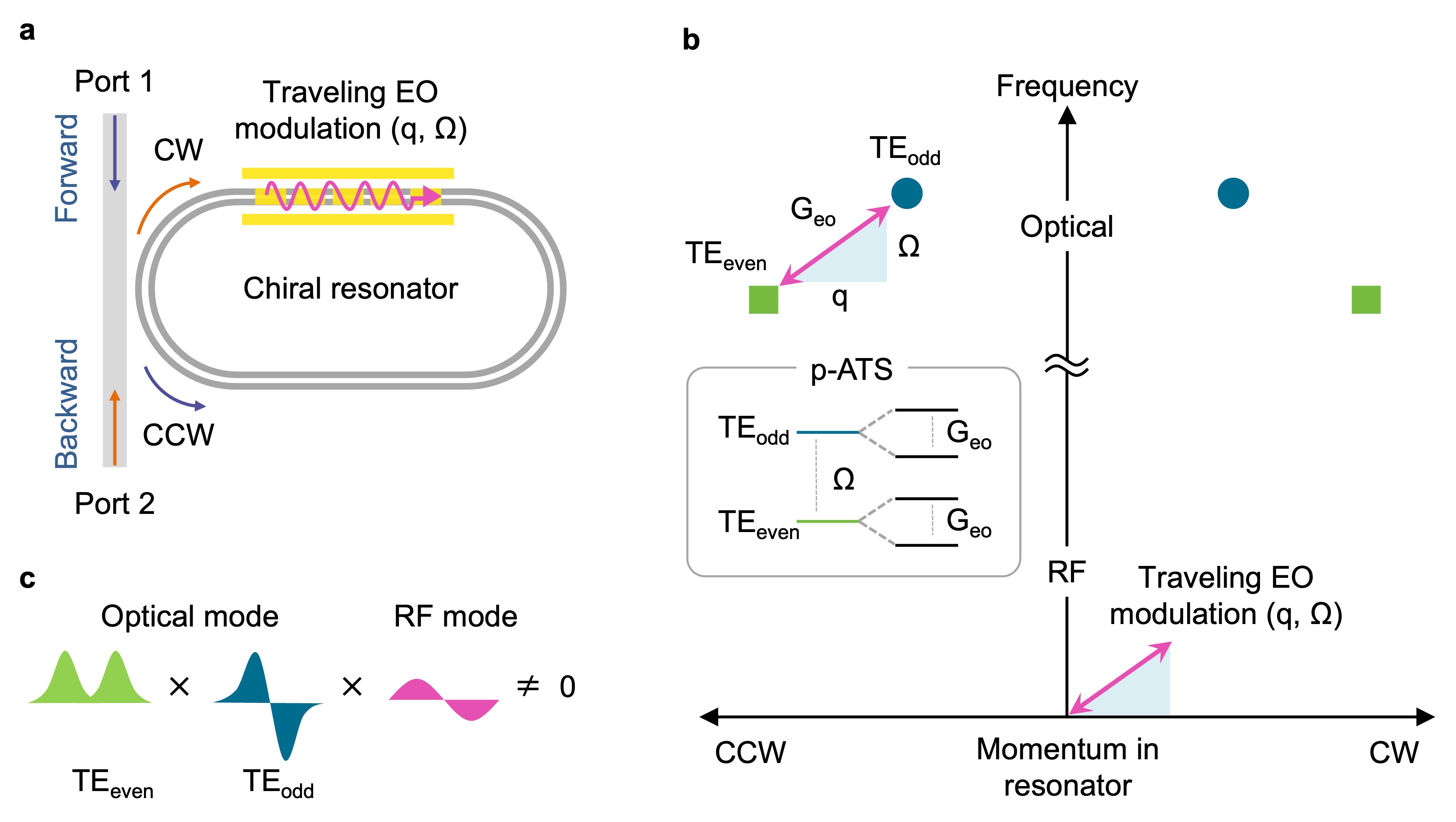
At the core of this isolator is a two-level “photonic atom” [zhang_electronically_2019] whose optical density of states (DoS) exhibits large chiral asymmetry due to an induced photonic Autler-Townes splitting (p-ATS) effect [peng_what_2014, kim_complete_2017, shi_nonreciprocal_2018, zhang_electronically_2019, sohn_electrically_2021]. This photonic atom is shunt coupled to a bus waveguide to produce isolation (Fig. 1a). A straightforward approach to producing the photonic atom is with a whispering gallery or racetrack resonator that supports only two non-degenerate optical mode families with distinct dispersions. A unidirectional stimulus with non-zero propagating momentum is then applied to the resonator, ensuring that the phase-matching for inter-modal conversion is only satisfied for one direction of propagation (Fig. 1b). When the stimulus-induced coupling rate , where are the loss rates for the individual optical modes, the system enters the strong coupling regime where the non-degenerate optical modes are hybridized and exhibit splitting, analogous to the splitting of electronic states in the conventional ATS phenomenon. Importantly, this p-ATS effect modifies the optical DoS only for the phase-matched direction [sohn_electrically_2021, kim_complete_2017, shi_nonreciprocal_2018]. For the counter-propagating direction, the original optical DoS remains unmodified. The previous AO implementations of this concept used single input propagating acoustic wave [sohn_electrically_2021] and 3-input acoustic standing wave [tian_magnetic-free_2021] stimuli to accomplish the phase-matching. Here we aim to replace this with an EO stimulus to facilitate tuning and encapsulation. However, the major challenge is that, unlike acoustic phonons which possess substantial momentum [sohn_electrically_2021, kittlaus_electrically_2020], RF traveling waves have very high phase velocity and are unable to bridge the required momentum gaps at practical frequencies.
-1in-1in
Our solution is to invoke a periodic EO modulator that generates a synthetic stimulus momentum [orsel_electro-optic_2023]. This approach also alleviates the phase-matching challenge across a wide spectrum by making the frequency a “free choice” variable that can be selected appropriately during operation. The schematic for our specific modulator is shown later in Fig. 2d, where a controlled relative phase shift is applied between subsequent electrodes having pitch . This configuration establishes a dominant spatial wavenumber of . The stimulus momentum is therefore set by an initial lithographic choice of , while the stimulus frequency is freely selectable during operation.
The next major requirement is to ensure a fixed azimuthal momentum separation between the optical mode pairs over a wide spectral range. The previous AO designs [sohn_electrically_2021, tian_magnetic-free_2021] required precise dimension control of the resonator to obtain the required momentum separation between the modes, but this causes the device yield to be very sensitive to small fabrication variations. Moreover, since the optical dispersions are different, the phase matching in a selected device is only achievable between a limited set of optical mode pairs, which restricts dynamic tuning of the isolation wavelength. Accordingly, our second key innovation is to instead use a double-racetrack resonator [xu_mutual-coupling_2022, zhang_broadband_2022], composed of identical component waveguides having identical underlying dispersion (Fig. 2a). This allows us to very easily control the momentum separation of the TEeven and TEodd optical modes (Fig. 2b) across a very wide spectrum, even though the frequency separation can vary slightly (as seen later in Fig. 5a). The combination of the above two design features – the freedom to choose the stimulus frequency, and the very steady momentum separation – enables the isolation effect to be coarsely tuned to optical mode pairs across a very wide spectral range.
Finally, the RF stimulus needs to be designed so that it breaks orthogonality (Fig. 1c) between the TEeven and TEodd modes via the nonlinearity. This is interpreted as a non-zero overlap integral between the optical modes and the RF stimulus, which is mathematically expressed as:
| (1) |
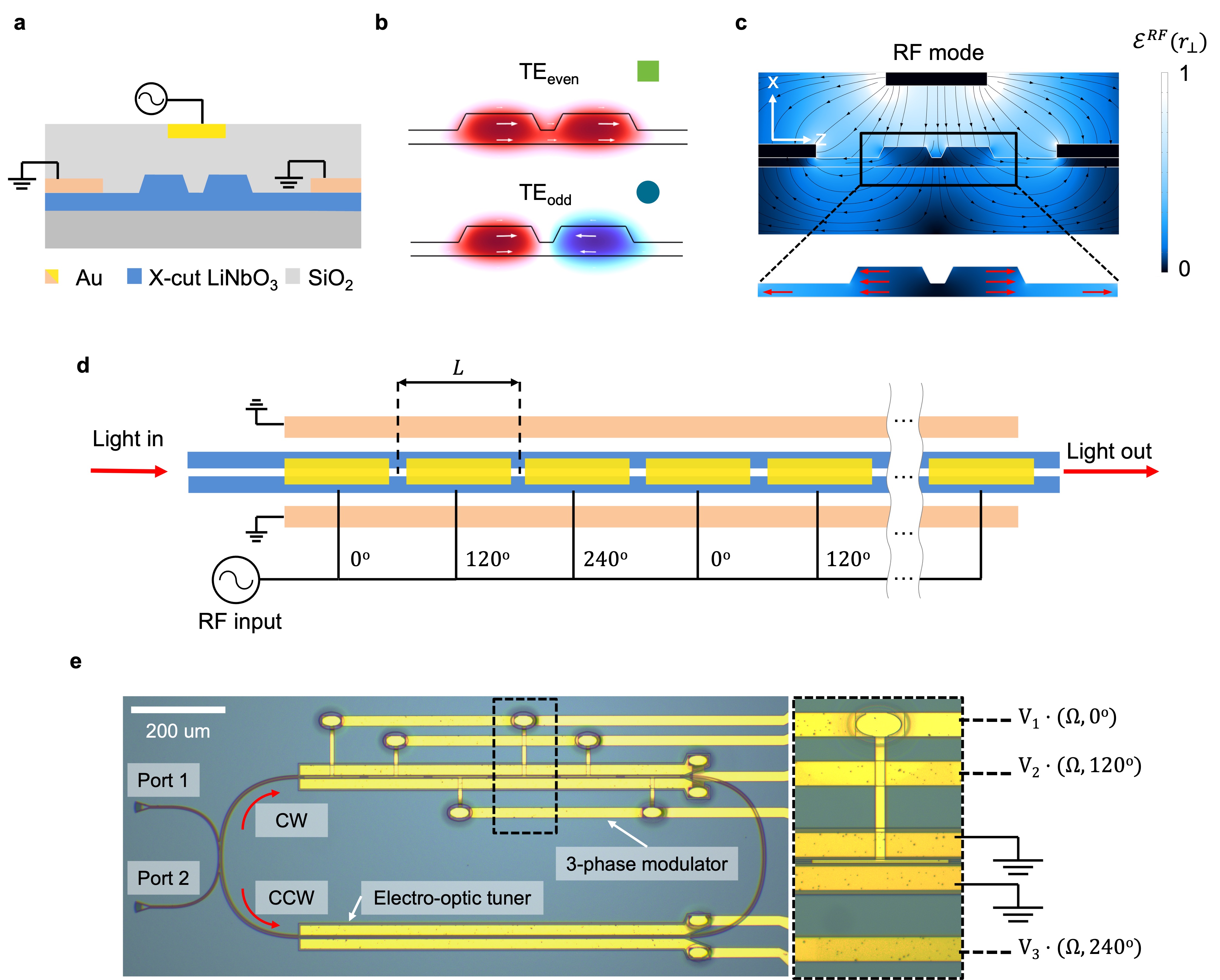
where , , and are the transverse field distribution of optical and RF modes respectively (Fig. 2b,c) and the subscripts refer to coordinate axes for the electro-optic tensor (the mathematical details are presented in [orsel_electro-optic_2023]). For our specific device, the best RF electrode configuration requires a two-layer structure. The lower layer supports the uninterrupted ground electrodes while the upper layer is split into the multi-phase stimulus electrode (Fig. 2a,d).
Results
We fabricated this optical isolator (Fig. 2e) using a 600 nm X-cut thin-film lithium niobate on insulator (TFLN) integrated photonics platform with an oxide cladding and two-layer gold electrodes to generate the required electro-optic stimuli. The fabrication process and key geometric features are described in Methods. Lithium niobate is well-suited for electro-optics due to its large EO coefficient ( pm/V) and wide bandgap, offering a broad transparency range of 250 to 5300 nm with propagation losses below 0.1 dB/cm [weis_lithium_1985, desiatov_ultra-low-loss_2019]. The resonator design targets an optical momentum gap of 13000 – 15000 rad/m. Accordingly, two periods of the 3-phase RF stimulus electrodes were patterned on one side of the resonator, and their pitch was selected at µm, resulting in a total interaction length of 900 µm. The stimulus electrode cross-section (Fig. 2a) was designed to generate a mirror-symmetric transverse electric field profile along the LN Z-axis (Fig. 2c) to efficiently harness the coefficient for modulation. We additionally fabricated a set of EO tuning electrodes on the opposite side of the resonator.
-1in-1in
-1in-1in
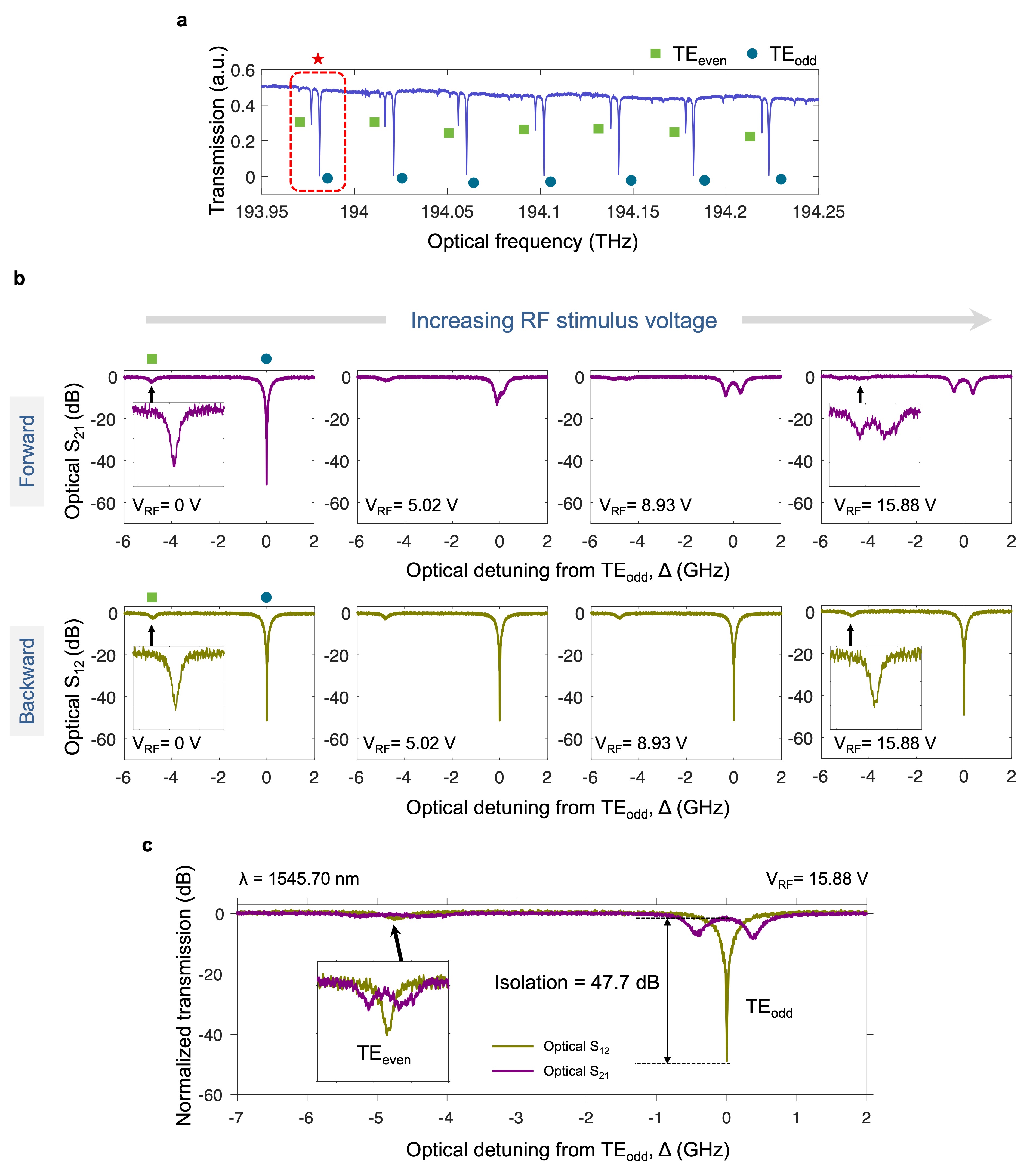
Demonstration of electro-optic isolation – Fig. 3 presents an example experiment on the isolator. First, we measured optical transmission through the waveguide in the telecom band, around 1550 nm, which reveals two distinct optical mode families of the resonator (Fig. 3a) with separation of a few GHz. The modes can be identified as TEeven and TEodd based on both coupling to the waveguide and their dispersive effect supported through finite element simulations. Next, we experimentally measure the through-waveguide transmission using a heterodyne detection system (see Methods) which enables resolved measurements on the carrier transmission, as well as any sideband signals that are generated. In this experiment we chose an optical mode pair near 193.98 THz (1545.50 nm) as identified in Fig. 3a with frequency gap of approximately 4.8 GHz and individual loss rates GHz and 0.53 GHz. We accordingly apply a 3-phase RF stimulus at GHz to the electrodes. Fig. 3b presents the evolution of the optical transmission through waveguide as a function of RF voltage (i.e. sinusoidal amplitude of RF stimulus, VRF) for both forward and backward directions. Here, we have we arbitrarily set the TEodd mode as the zero detuning reference point () for the optical frequency axis. In the absence of any applied RF, the transmission function remains identical in both directions. However, with increasing RF voltage, the p-ATS modal hybridization appears for one direction of propagation only. In Fig. 3c we present a superimposed result at the highest applied RF amplitude of 15.88 V, reaching a peak isolation contrast of 47.7 dB with a forward insertion loss of 1.45 dB. This implies IC/IL ratio of dB/dB which makes the performance comparable to commercial magneto-optic isolators. By fitting to coupled mode theory [sohn_electrically_2021], we determine that this driving condition corresponds to an EO coupling rate GHz. We measure a 10 dB IC bandwidth of MHz and 20 dB IC bandwidth of MHz. We tested this device with an estimated in-waveguide optical power up to 5 mW.
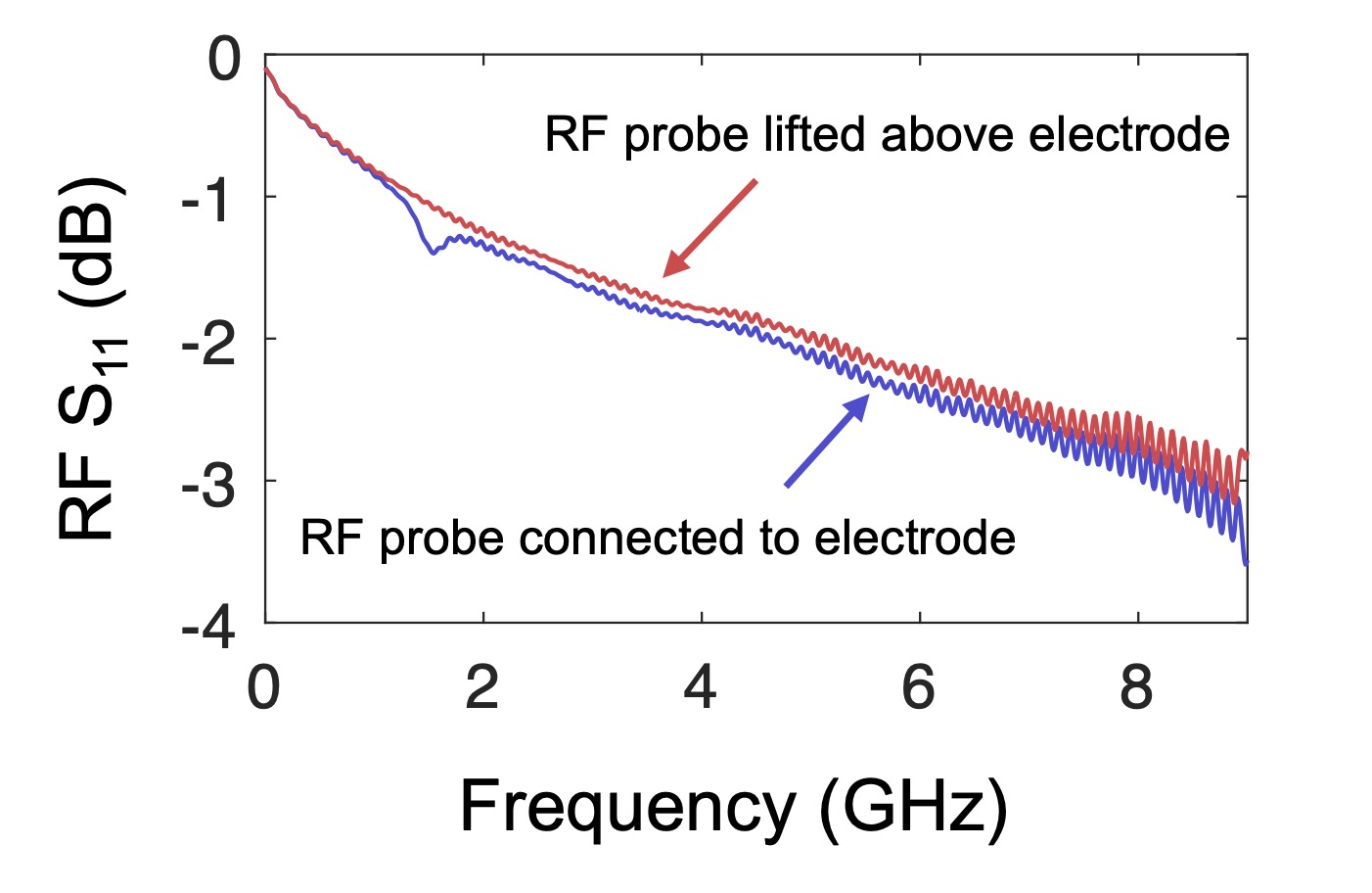
While the EO stimulus on this device has an overall traveling wave characteristic, the propagating momentum is generated only synthetically. We confirm this using a RF S11 reflection measurement at the stimulus electrodes (Supplementary Data Figure 2) which confirms their uniformly high reflection and open circuit (capacitive) behavior [orsel_electro-optic_2023]. The residual loss arises from propagation in the measurement cables. For the specific experiment in Fig. 3, the bench-top signal generator power was set at 28 dBm (630 mW), and the RF S11 measurement at 4.8 GHz informs us of a fundamental upper limit of only 12.9 mW (11.09 dBm) power consumed by the device. With improved RF design and a custom source, the power consumption can be reduced significantly. Thus, essentially all of the signal generator voltage (15.88 V) appears directly on the stimulus electrodes due to the open circuit.
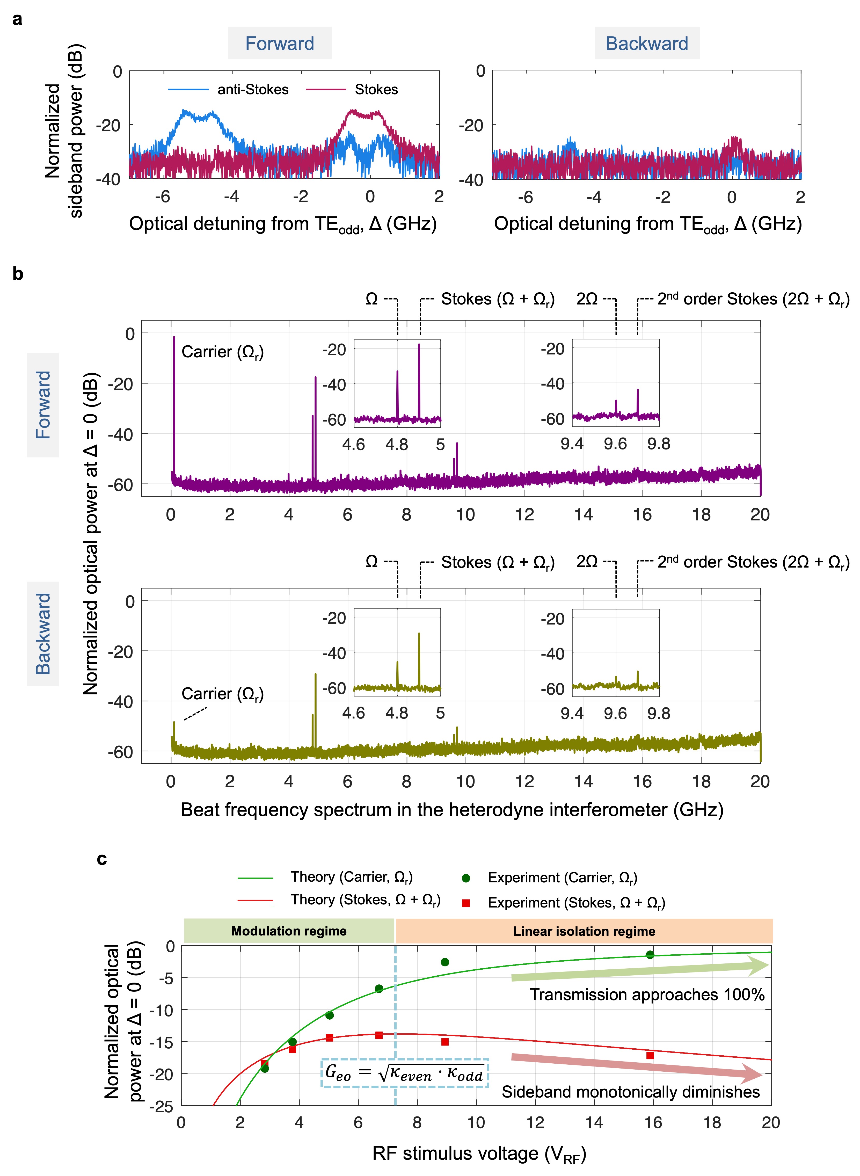
Sideband analysis – During experiments we also monitored the anti-Stokes and Stokes sidebands since they are a concern in non-reciprocal devices that use strong spatio-temporal modulation [doerr_optical_2011, doerr_silicon_2014, yu_integrated_2023, gao_thin-film_2024]. Fig. 4a presents measurements of the first-order sidebands as a function of optical detuning , under the operational conditions of Fig. 3c. Naturally, the sideband generation in the forward (phase-matched) direction is shaped by the optical DoS as modified by the p-ATS. In the limit of very strong coupling, the p-ATS dressed states will be fully resolved [kim_complete_2017], and at the optical DoS will reach zero causing the forward direction first-order sideband to be eliminated. In the backward (not phase-matched) direction the sidebands are significantly smaller.
Fig. 4b analyzes the higher-order sidebands in the optical spectrum using the heterodyne interferometer (see Methods and Supplementary Data Figure 1) with the input laser centered on the TEodd mode () and reference arm frequency shift of MHz. We expect that only first-order Stokes scattering will be notable since only scattering to TEeven can take place. The interferometer spectrum shows the carrier (at ), first Stokes (at ), and a much smaller second-order Stokes (at ) signal. We normalize the forward and backward measurements relative to the carrier transmission in the forward direction. These measurements confirm that only the first Stokes sideband is of significance. The first anti-Stokes () and second anti-Stokes () are absent, or below the noise floor, as there are no optical states available within the resonator.
These sideband generation behaviors are readily predictable from coupled mode theory [sohn_electrically_2021, kim_complete_2017] and two regimes of operation have been identified. When the applied stimulus is small, the device acts as a non-reciprocal frequency shifting modulator [sohn_time-reversal_2018]. However, once the device enters the strong coupling or p-ATS regime where linear isolation becomes available. With increasing drive level the p-ATS dressed states get resolved further and the ideality of the device monotonically improves as sideband generation reduces monotonically. This behavior and the close match between experiments and theory is confirmed in Fig. 4c.
-1in-1in

Tunability across a wide spectrum – We additionally confirmed the tuning capability of this EO isolator over the range 193.35 – 194.45 THz (approximately 8 nm from 1542 – 1550 nm). For all the mode pairs shown in Fig. 5a, we identify the frequency gap as it changes slightly across the spectrum even though the azimuthal momentum spacing within any mode pair must be the same. We then apply the corresponding 3-phase RF stimulus at that with V. This is possible since, as mentioned earlier, the frequency is a completely free variable in this EO design. We observed that the isolator maintains dB contrast and dB insertion loss for all mode pairs across this spectral range, confirming consistent optical isolation performance. Thus, each mode pair indicates a coarse tuning choice for the isolator.
Finally, we explore the possibility of fine-tuning to fill the spectral gaps between the coarse tuning points. We measure that a dc voltage on the EO tuning electrodes (see Supplementary Data Fig. 3) linearly shifts both modes of a pair together (Fig. 5b). For the device tested the tuning capability was measured at 0.20 GHz/V for the TEodd mode and 0.21 GHz/V for the TEeven mode, with the difference arising due to the distinction of modal group index. The small monotonic change in the frequency gap can be tracked while tuning the device to appropriately adjust the stimulus frequency . Since the free spectral range between optical mode pairs in this device is around GHz, an application of 100 VDC can tune the modes to completely cover the gaps. We leave further improvements on the tuning structure to future efforts, since the resonator free spectral range can be reduced by simple redesign, and we additionally note that the combination of EO tuning and stress-based piezoelectric tuning [tian_piezoelectric_2024] could provide enhanced tuning capability.
Discussion
This EO isolator delivers dB/dB isolator figure-of-merit while using nearly 20x smaller interaction length (900 µm here, vs 1.75 cm) and requires nearly 10x lower RF input power than the best comparable EO isolator (12.5 mW here, vs 125 mW) [yu_integrated_2023]. This is because the stimulus electrodes do not draw RF power from the signal generator, but merely act as open-circuited capacitors. Also, this design consumes nearly 64x lower RF input power than the best comparable performance AO p-ATS isolator of similar design (794 mW) [sohn_electrically_2021]. The efficiency of our device can be improved further by incorporating more periods of the EO stimulus electrodes around the resonator resulting in a larger interaction length. The EO tuning could then be performed using these same stimulus electrodes but with two different dc ground offset voltages. As with the AO p-ATS isolator, our EO p-ATS design has an instantaneous isolation bandwidth that is fundamentally set by the optical modes, though that could be improved somewhat by lowering the optical Q-factors while simultaneously increasing . We also showed that very wide tuning capability is enabled thanks to dual innovations on a double-racetrack resonator design and a synthetic momentum approach, both of which together relax the phase-matching constraints. Most importantly, the p-ATS approach intrinsically produces minimal sidebands, but which also improve monotonically as the stimulus level is increased. Thus, future modulation efficiency enhancements with novel materials like BaTiO3 [dong_monolithic_2023, demkov_ferroelectric_2024, mohl_bidirectional_2025] could improve ideality and performance metrics even further. Another approach to reduce the residual sideband is to fully decouple the auxiliary TEeven mode from the waveguide by means of smart optical design. Ultimately, these narrowband but widely tunable non-magnetic isolators can have a big positive impact for single-frequency protection, e.g. for ultrastable laser sources [poulton_coherent_2017, spencer_optical-frequency_2018, lucas_ultralow-noise_2020], atomic references [knappe_microfabricated_2004, hummon_photonic_2018, newman_architecture_2019], and optical metrology [delhaye_optical_2007].
Methods
Device fabrication – The starting substrate was X-cut thin film lithium niobate on 2 µm silicon dioxide on a silicon handle wafer. Optical components were patterned using a 150 keV electron beam lithography (EBL, Elionix ELS-G150) system and the thin film lithium niobate was etched down by 300 nm (approximately 60 degree sidewalls) via argon inductively coupled plasma reactive ion etch (ICP-RIE). The double-racetrack resonator was designed using identical concentric waveguides, each having width 1.2 µm and gap of 650 nm between them. Lower electrodes were defined by EBL using 200 nm gold deposited through e-beam evaporation and lift-off process, and placed 3 µm away from the edge of the double racetrack resonator. A 2 µm silicon dioxide (SiO2) cladding layer was deposited using plasma enhanced chemical vapor deposition (PECVD). Metal via holes were created in the cladding using buffered oxide etching. Top electrodes were finally patterned by depositing an additional 400 nm gold layer via e-beam evaporation and lift-off process.
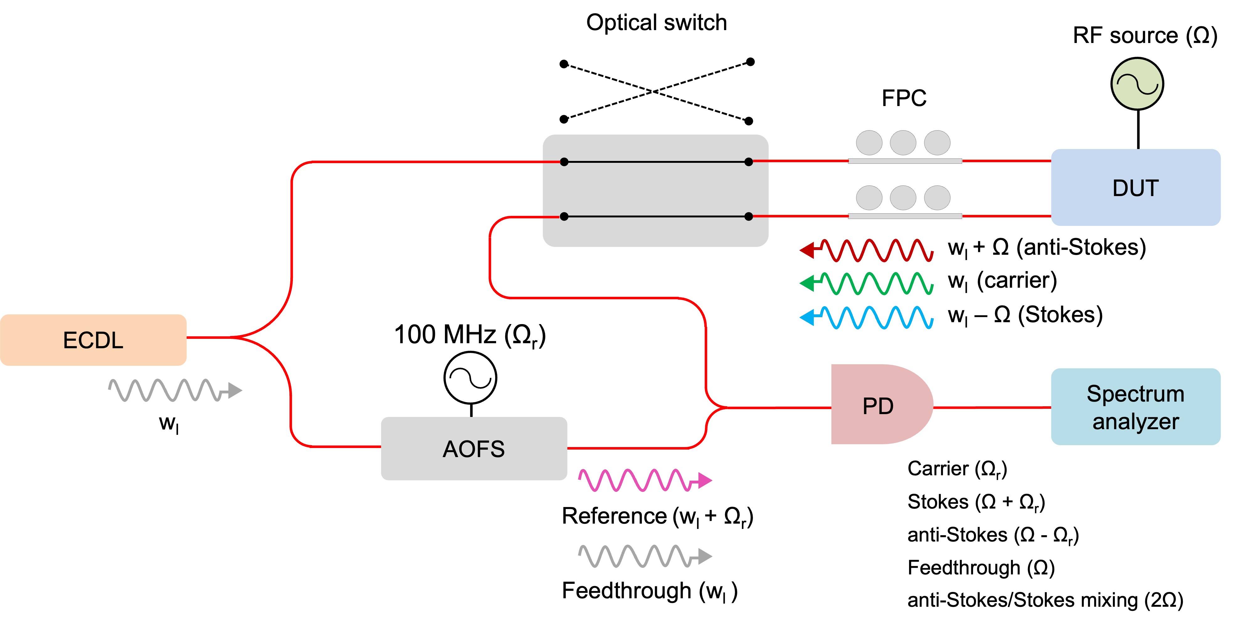
Heterodyne measurement system – We measure the carrier and sidebands using a heterodyne interferometer (Supplementary Data Fig. 1) which was described in [sohn_electrically_2021]. A tunable external cavity diode laser (New Focus TLB-6712-P), operating within the 1520–1570 nm range and featuring a sub-50 kHz linewidth, was utilized as the light source. An acousto-optic frequency shifter (Brimrose TEF-200-780-2FP) was employed to generate a reference signal for frequency-resolved characterization of the carrier and sidebands, which were analyzed using a high-speed photodetector (Thorlabs RXM25DF). Probe direction was managed via an off-chip optical switch (Thorlabs OSW22-780E). The optical beat signal was generated and analyzed using a 4-port vector network analyzer (Agilent ENA E5080A) and a real-time spectrum analyzer (Tektronix RSA5100B). RF signals were directly supplied by a multi-output synchronized microwave signal generator (Holzworth 9004).
References
- [1] Bi, L. et al. On-chip optical isolation in monolithically integrated non-reciprocal optical resonators. Nat. Photonics 5, 758 (2011). URL https://www.nature.com/articles/nphoton.2011.270.
- [2] Ghosh, S. et al. Ce:YIG/Silicon-on-Insulator waveguide optical isolator realized by adhesive bonding. Optics Express 20, 1839 (2012). URL https://opg.optica.org/oe/abstract.cfm?uri=oe-20-2-1839.
- [3] Huang, D. et al. Dynamically reconfigurable integrated optical circulators. Optica 4, 23 (2017). URL https://opg.optica.org/abstract.cfm?URI=optica-4-1-23.
- [4] Zhang, Y. et al. Monolithic integration of broadband optical isolators for polarization-diverse silicon photonics. Optica 6, 473 (2019). URL https://opg.optica.org/abstract.cfm?URI=optica-6-4-473.
- [5] Du, Q. et al. Monolithic On-chip Magneto-optical Isolator with 3 dB Insertion Loss and 40 dB Isolation Ratio. ACS Photonics 5, 5010–5016 (2018). URL https://pubs.acs.org/doi/10.1021/acsphotonics.8b01257.
- [6] Yan, W. et al. Waveguide-integrated high-performance magneto-optical isolators and circulators on silicon nitride platforms. Optica 7, 1555 (2020). URL https://opg.optica.org/abstract.cfm?URI=optica-7-11-1555.
- [7] Yan, W. et al. Ultra-broadband magneto-optical isolators and circulators on a silicon nitride photonics platform. Optica 11, 376 (2024). URL https://opg.optica.org/abstract.cfm?URI=optica-11-3-376.
- [8] Hwang, I. K., Yun, S. H. & Kim, B. Y. All-fiber-optic nonreciprocal modulator. Optics Letters 22, 507 (1997). URL https://opg.optica.org/abstract.cfm?URI=ol-22-8-507.
- [9] Sohn, D. B., Kim, S. & Bahl, G. Time-reversal symmetry breaking with acoustic pumping of nanophotonic circuits. Nature Photonics 12, 91–97 (2018). URL https://www.nature.com/articles/s41566-017-0075-2.
- [10] Kittlaus, E. A. et al. Electrically driven acousto-optics and broadband non-reciprocity in silicon photonics. Nature Photonics 15, 43–52 (2020). URL https://www.nature.com/articles/s41566-020-00711-9.
- [11] Sohn, D. B., Örsel, O. E. & Bahl, G. Electrically driven optical isolation through phonon-mediated photonic Autler–Townes splitting. Nature Photonics 15, 822–827 (2021). URL https://www.nature.com/articles/s41566-021-00884-x.
- [12] Tian, H. et al. Magnetic-free silicon nitride integrated optical isolator. Nature Photonics 15, 828–836 (2021). URL https://www.nature.com/articles/s41566-021-00882-z.
- [13] Bhandare, S. et al. Novel nonmagnetic 30-dB traveling-wave single-sideband optical isolator integrated in III/V material. IEEE Journal of Selected Topics in Quantum Electronics 11, 417–421 (2005). URL http://ieeexplore.ieee.org/document/1425478/.
- [14] Doerr, C. R., Dupuis, N. & Zhang, L. Optical isolator using two tandem phase modulators. Optics Letters 36, 4293 (2011). URL https://opg.optica.org/abstract.cfm?URI=ol-36-21-4293.
- [15] Lira, H., Yu, Z., Fan, S. & Lipson, M. Electrically Driven Nonreciprocity Induced by Interband Photonic Transition on a Silicon Chip. Physical Review Letters 109, 033901 (2012). URL https://link.aps.org/doi/10.1103/PhysRevLett.109.033901.
- [16] Tzuang, L. D., Fang, K., Nussenzveig, P., Fan, S. & Lipson, M. Non-reciprocal phase shift induced by an effective magnetic flux for light. Nature Photonics 8, 701–705 (2014). URL https://www.nature.com/articles/nphoton.2014.177.
- [17] Doerr, C. R., Chen, L. & Vermeulen, D. Silicon photonics broadband modulation-based isolator. Optics Express 22, 4493 (2014). URL https://opg.optica.org/oe/abstract.cfm?uri=oe-22-4-4493.
- [18] Dostart, N., Gevorgyan, H., Onural, D. & Popovifá, M. A. Optical isolation using microring modulators. Optics Letters 46, 460 (2021). URL https://opg.optica.org/abstract.cfm?URI=ol-46-3-460.
- [19] Yu, M. et al. Integrated electro-optic isolator on thin-film lithium niobate. Nature Photonics 17, 666–671 (2023). URL https://www.nature.com/articles/s41566-023-01227-8.
- [20] Örsel, O. E. & Bahl, G. Electro-optic non-reciprocal polarization rotation in lithium niobate. APL Photonics 8, 096107 (2023). URL https://pubs.aip.org/app/article/8/9/096107/2911672/Electro-optic-non-reciprocal-polarization-rotation.
- [21] Gao, L. et al. Thin-film lithium niobate electro-optic isolator fabricated by photolithography assisted chemo-mechanical etching. Optics Letters 49, 614 (2024). URL https://opg.optica.org/abstract.cfm?URI=ol-49-3-614.
- [22] Örsel, O. E. et al. Giant non-reciprocity and gyration through modulation-induced Hatano-Nelson coupling in integrated photonics (2024). URL http://arxiv.org/abs/2410.10079. ArXiv:2410.10079 [physics].
- [23] Zhang, M. et al. Electronically programmable photonic molecule. Nature Photonics 13, 36–40 (2019). URL https://www.nature.com/articles/s41566-018-0317-y.
- [24] Peng, B., Özdemir, Ş. K., Chen, W., Nori, F. & Yang, L. What is and what is not electromagnetically induced transparency in whispering-gallery microcavities. Nature Communications 5, 5082 (2014). URL https://www.nature.com/articles/ncomms6082.
- [25] Kim, J., Kim, S. & Bahl, G. Complete linear optical isolation at the microscale with ultralow loss. Sci. Rep. 7, 1647 (2017). URL https://www.nature.com/articles/s41598-017-01494-w.
- [26] Shi, Y., Lin, Q., Minkov, M. & Fan, S. Nonreciprocal Optical Dissipation Based on Direction-Dependent Rabi Splitting. IEEE Journal of Selected Topics in Quantum Electronics 24, 1–7 (2018). URL https://ieeexplore.ieee.org/document/8310902/.
- [27] Xu, Y., Liu, T., Liu, S., Sun, X. & Zhang, D. Mutual-Coupling in High-Q Silicon Dual-Concentric Micro-Ring/Racetrack Resonator. IEEE Photonics Journal 14, 1–7 (2022). URL https://ieeexplore.ieee.org/document/9809804/.
- [28] Zhang, Y., Zhong, K., Zhou, X. & Tsang, H. K. Broadband high-Q multimode silicon concentric racetrack resonators for widely tunable Raman lasers. Nature Communications 13, 3534 (2022). URL https://www.nature.com/articles/s41467-022-31244-0.
- [29] Weis, R. S. & Gaylord, T. K. Lithium niobate: Summary of physical properties and crystal structure. Applied Physics A Solids and Surfaces 37, 191–203 (1985). URL http://link.springer.com/10.1007/BF00614817.
- [30] Desiatov, B., Shams-Ansari, A., Zhang, M., Wang, C. & Lonfçar, M. Ultra-low-loss integrated visible photonics using thin-film lithium niobate. Optica 6, 380 (2019). URL https://opg.optica.org/abstract.cfm?URI=optica-6-3-380.
- [31] Tian, H. et al. Piezoelectric actuation for integrated photonics. Advances in Optics and Photonics 16, 749 (2024). URL https://opg.optica.org/abstract.cfm?URI=aop-16-4-749.
- [32] Dong, Z. et al. Monolithic Barium Titanate Modulators on Silicon-on-Insulator Substrates. ACS Photonics 10, 4367–4376 (2023). URL https://pubs.acs.org/doi/10.1021/acsphotonics.3c01144.
- [33] Demkov, A. A. & Posadas, A. B. Ferroelectric BaTiO for Electro-Optic Modulators in Si Photonics. IEEE Journal of Selected Topics in Quantum Electronics 30, 1–13 (2024). URL https://ieeexplore.ieee.org/document/10538359/.
- [34] Möhl, C. et al. Bidirectional microwave-optical conversion with an integrated soft-ferroelectric barium titanate transducer (2025). URL http://arxiv.org/abs/2501.09728. ArXiv:2501.09728 [physics].
- [35] Poulton, C. V. et al. Coherent solid-state LIDAR with silicon photonic optical phased arrays. Optics Letters 42, 4091 (2017). URL https://opg.optica.org/abstract.cfm?URI=ol-42-20-4091.
- [36] Spencer, D. T. et al. An optical-frequency synthesizer using integrated photonics. Nature 557, 81–85 (2018). URL https://www.nature.com/articles/s41586-018-0065-7.
- [37] Lucas, E. et al. Ultralow-noise photonic microwave synthesis using a soliton microcomb-based transfer oscillator. Nature Communications 11, 374 (2020). URL https://www.nature.com/articles/s41467-019-14059-4.
- [38] Knappe, S. et al. A microfabricated atomic clock. Applied Physics Letters 85, 1460–1462 (2004). URL https://pubs.aip.org/apl/article/85/9/1460/116970/A-microfabricated-atomic-clock.
- [39] Hummon, M. T. et al. Photonic chip for laser stabilization to an atomic vapor with 10 instability. Optica 5, 443 (2018). URL https://opg.optica.org/abstract.cfm?URI=optica-5-4-443.
- [40] Newman, Z. L. et al. Architecture for the photonic integration of an optical atomic clock. Optica 6, 680 (2019). URL https://opg.optica.org/abstract.cfm?URI=optica-6-5-680.
- [41] Del’Haye, P. et al. Optical frequency comb generation from a monolithic microresonator. Nature 450, 1214–1217 (2007). URL https://www.nature.com/articles/nature06401.
Acknowledgments
This work was sponsored by the Defense Advanced Research Projects Agency (DARPA) under Cooperative Agreement D24AC00003, the Air Force Research Laboratory (AFRL) / US Space Force (USSF) grant FA9453-20-2-0001, and the US Office of Naval Research (ONR) Multi-University Research Initiative grant N00014-20-1-2325. The views and conclusions contained herein are those of the authors and should not be interpreted as necessarily representing the official policies or endorsements, either expressed or implied, of DARPA, AFRL, ONR, or the US Government. The authors would like to acknowledge invaluable support from Dr. Brian Kasch at the Air Force Research Laboratory, Space Vehicles Directorate, and Dr. Edmond Chow and Amr O. Ghoname at the Holonyak Micro & Nanotechnology Lab (HMNTL) at University of Illinois at Urbana-Champaign.
-1in-1in
-1in-1in
-1in-1in
| Author | Year | Device | Technique | Isolation contrast (IC) | Insertion loss (IL) | IC/IL (dB/dB) |
| This work | - | Resonator | EO | 47.7 dB | 1.45 dB | 32.9 |
| Yu et. al. [yu_integrated_2023] | 2023 | Waveguide | EO | 48 dB | 1.4 dB (w/ filter) | 34.28 |
| 0.5 dB (w/o necessary filter) | 96 | |||||
| Gao et. al. [gao_thin-film_2024] | 2023 | Waveguide | EO | 39.5 dB | 2.6 dB (w/o filter) | 15.19 |
| Dostart et. al. [dostart_optical_2021] | 2021 | Resonator | EO | 13.1 dB | 18.1 dB | 0.18 |
| Doerr et. al. [doerr_silicon_2014] | 2014 | Waveguide | EO | 6 dB | 4 dB | 0.66 |
| Tzuang et. al. [tzuang_non-reciprocal_2014] | 2014 | Waveguide | EO | 2.4 dB | N/A | N/A |
| Lira et. al. [lira_electrically_2012] | 2012 | Waveguide | EO | 3 dB | 70 dB | 0.04 |
| Doerr et. al. [doerr_optical_2011] | 2011 | Waveguide | EO | 2 dB | 11 dB | 0.18 |
| Bhandare et. al. [bhandare_novel_2005] | 2005 | Waveguide | EO | 30 dB | 8 dB | 3.75 |
| Sohn et. al. [sohn_electrically_2021] | 2021 | Resonator | AO | 39.31 dB | 0.65 dB | 60.46 |
| 12.75 dB | 1.13 dB | 11.28 | ||||
| Tian et. al. [tian_magnetic-free_2021] | 2021 | Resonator | AO | 9.3 dB | 0.8 dB | 11.62 |
| 41 dB | 1.9 dB | 21.57 |