Fabrication and Characterization of Impedance-transformed Josephson Parametric Amplifier
Abstract
In this paper, we introduce a method of using a double-layer resist lift-off process to prepare the capacitor dielectric layer for fabricating impedance-engineered Josephson parametric amplifiers (IMPAs). Compared with traditional techniques, this method enhances fabrication success rate, accelerates production. The IMPA we made experimentally achieves an instantaneous bandwidth over 950 (600) MHz with a gain exceeding 10 (14) dB, along with saturation input power of -115 dBm and near quantum-limited noise. We demonstrate the negligible backaction from the IMPA on superconducting qubits, resulting in no significant degradation of the relaxation time and coherence time of the qubits. The IMPA improves the signal-to-noise ratio from 1.69 to 14.56 and enables the amplification chain to achieve a high quantum efficiency with , making it a critical necessity for large-scale quantum computation.
pacs:
42.50.Dv, 42.50.ExQuantum-limitedCaves (1982) Josephson parametric amplifiers (JPAs) play a key role in experiments for detection of single-photon-level microwave signals in the field of circuit quantum electrodynamics. Featured applications include single-shot readout,Lin et al. (2013); Abdo et al. (2011); Walter et al. (2017) feedback control of superconducting qubits,Vijay et al. (2012); Ristè et al. (2013) and the generation of squeezed quantum states.Yurke (1987); Castellanos-Beltran et al. (2008) Despite extensive research on Josephson parametric amplifiers over the past decades,Mooij et al. (1999); You, Tsai, and Nori (2003); Koch et al. (2007a); Yamamoto et al. (2008); Reed et al. (2010); Hatridge et al. (2011); Lucero et al. (2012); Barends et al. (2013); Zhong et al. (2013) their limited bandwidth and dynamic range have constrained their applicability in the rapidly advancing field of multi-qubit architectures and the realization of fault-tolerant quantum computation.Chen et al. (2012); Fowler et al. (2012); Barends et al. (2014)
In recent years, a variety of schemes have been proposed to enhance the bandwidth and dynamic range of parametric amplifiers.Roy et al. (2015); Esposito et al. (2021); Macklin et al. (2015); Mutus et al. (2014); Duan et al. (2021) One scheme is the Josephson traveling-wave parametric amplifier (JTWPA), which achieves a bandwidth over several gigahertz with a gain exceeding 20 dB, making it suitable for the simultaneous readout of multiple qubits.Macklin et al. (2015) However, this scheme requires the fabrication of thousands of nearly identical Josephson junctions, which significantly reduces the overall fabrication success rate of the device. Moreover, the strict requirements on phase matching make the design, fabrication and calibration of JTWPA difficult.Esposito et al. (2021)
Another scheme is the impedance-engineered Josephson parametric amplifier (IMPA), which focuses on designing the environmental impedance to enhance the coupling of the JPA to the environment and reduce the quality factor of the Josephson oscillator, resulting in improving the bandwidth and saturation power.Roy et al. (2015); Mutus et al. (2014); Duan et al. (2021) In one method, A lumped-element Josephson parametric amplifier was introduced, designed to achieve strong environmental coupling via a tapered transmission line.Mutus et al. (2014) This method successfully broadens the bandwidth and saturation power. However, engineering a tapered transmission line requires complex nano-fabrication. An alternative method of introducing one impedance transformer and one impedance transformer simplify the fabrication process and also achieves noteworthy performance.Roy et al. (2015); Duan et al. (2021) We adopt this methodDuan et al. (2021) and present a double-layer resist lift-off process to fabricate the capacitor dielectric layer of IMPA, which offers a higher success rate than traditional methods.
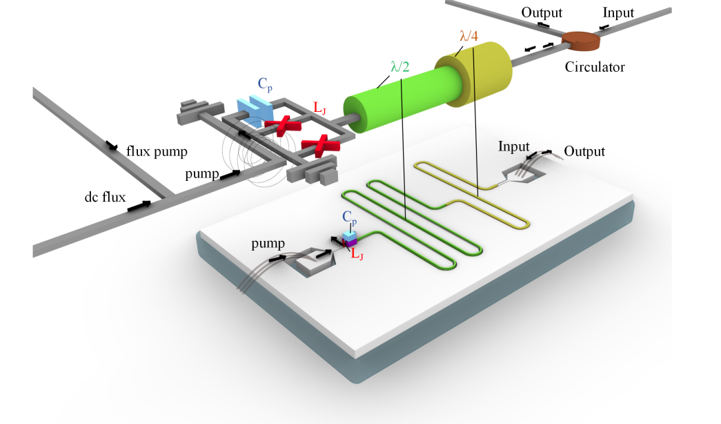
Figure 1a presents the 3D scheme and the circuit model of our device. The non-linear LC resonator is formed by a capacitor and a superconducting quantum interference device (SQUID) loop as a nonlinear inductor . The performance of the JPA is inherently limited by the weak coupling that exists between this nonlinear resonator and its external environment. To enhance the amplifier’s gain, Josephson nonlinear components and a coplanar-waveguide (CPW) transformer are integrated on the same chip,Duan et al. (2021) as depicted in Figure 1a. To begin with, a impedance transformer is employed to convert the standard ambient impedance from to . This transformation not only broadens the bandwidth but also reduces the value of . Subsequently, A co-planar waveguide resonator is introduced to induce a positive linear slope in the imaginary component of the impedance shunting the JPA, while maintaining the impedance at . This configuration modifies the coherent cavity dynamics, reducing the susceptibility to the effects of detuning the signal from the pump. In our design, the capacitor and the total critical current .
| Equipment | Device model |
|---|---|
| Maskless Lithography System | Heidelberg Instruments DWL66+ |
| Plasma Enhanced Chemical Vapor Deposition System | Oxford Instruments System100 PECVD |
| Inductively Coupled Plasma Reactive Ion Ecthing | Oxford Instruments Plasmalab System100 |
| Electron-Beam Lithography System | JOEL JBX-6300FS |
| Electron-Beam Evaporator System | Plassys MEB550SL3 |
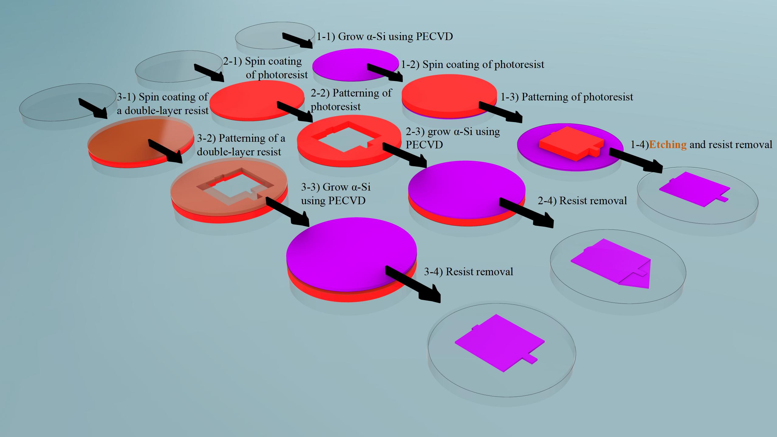
Our device is fabricated on a 430--thick, 2-inch diameter sapphire wafer with a (0001) orientation. The wafer undergoes thermal annealing at 200°C for 3 hours under high vacuum conditions and subsequently subjected to electron beam evaporation (EBD) to deposit a 100-nm-thick aluminum film. Then we pattern the aluminum film with laser direct writing and wet etching techniques, which defines the capacitor’s ground electrode and co-planar waveguide resonators. Subsequently, we proceed with the preparation of the dielectric layer of the capacitor. Initially, we adopt the method including a deposition of an amorphous silicon layer and then pattern it by etching,Mutus et al. (2014) illustrated in figure 1b as the first method. However, this method necessitates precise control of the etching rate of reactive ion etching (RIE), as improper control can lead to issues such as over-etching and under-etching. Over-etching can potentially induce damage to the aluminum film surface, thereby increasing electron scattering and thermal noise, which in turn reduces the signal-to-noise ratio. Under-etching, on the other hand, can leave residual dielectric material, which may interfere with the subsequent growth of SQUIDs. To address these challenges, we investigate alternative methods utilizing lift-off techniques. We finally choose the third method in figure 1b, a double-layer resist lift-off technique combined with plasma-enhanced chemical vapor deposition (PECVD), to fabracite 250-nm-thick amorphous silicon dielectric layer. Our findings reveal that the single-layer resist lift-off process is prone to defects, such as incomplete removal of the dielectric layer, which can adversely affect the electrical connection between the upper electrode and other components. Conversely, the double-layer resist lift-off process effectively substantially minimizes the accumulation of dielectric residues, thus leading to enhanced process reliability. Furthermore, the potential issue of protruding dielectric layer edges following the lift-off process is considered, as this could interfere with deposition on the upper electrode of the capacitor, thereby impeding proper electrical connection on either side of the protrusion. To address this concern, LOR3A and SPR955 are carefully selected from a range of photoresists, and their spin-coating speeds are precisely controlled to regulate the height of these protrusions. This ensures that the thickness of the aluminum film deposited on the upper electrode exceeds the height of the protrusions, which, results in preserving electrical continuity and improving the success rate of fabrication.
Subsequently, the upper electrode of the capacitor, consisting of a 300-nm-thick aluminum film, is also fabricated using the aforementioned double-layer resist lift-off technique. Ultimately, SQUIDs are fabricated using Dolan bridge shadow evaporation technique.Dolan (1977) A double-layer resist system is employed for the bridge fabrication, consisting of a methyl methacrylate (MMA) EL9 copolymer resist as the first layer and polymethyl methacrylate (PMMA) 950 A5 as the second layer. An in-situ argon ion milling process is essential for optimal electrical connectivity between the initial alumium layer and the SQUIDs. After the ion milling process, We utilize a standard double-angle evaporation technique to create trilayer structures as Josephson junctions. Several additional SQUIDs are integrated on the chip to verify that the resistance of the junction at ambient temperature is adequate. The types and specific models of instruments utilized in the fabrication process are presented in Table 1.
Our IMPA device is electrically interconnected to an aluminum sample holder through wire bonding, which is subsequently positioned within a magnetically shielded enclosure. The device is cooled to a 15mK base temperature inside a dilution refrigerator and worked in a reflection mode. A very weak signal ( -108 dBm to -132 dBm) is input into the measurement system, subsequently amplified and reflected. A 4-8 GHz cryogenic circulator, connected to the IMPA, is utilized to separate the reflected output signal and the input signal. The output signal undergoes further amplification through a commercial high-electron-mobility transistor (HEMT) amplifier operating at 4 K, followed by additional amplification at room temperature before digitization.
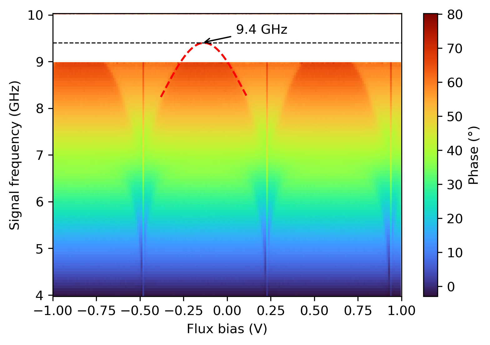
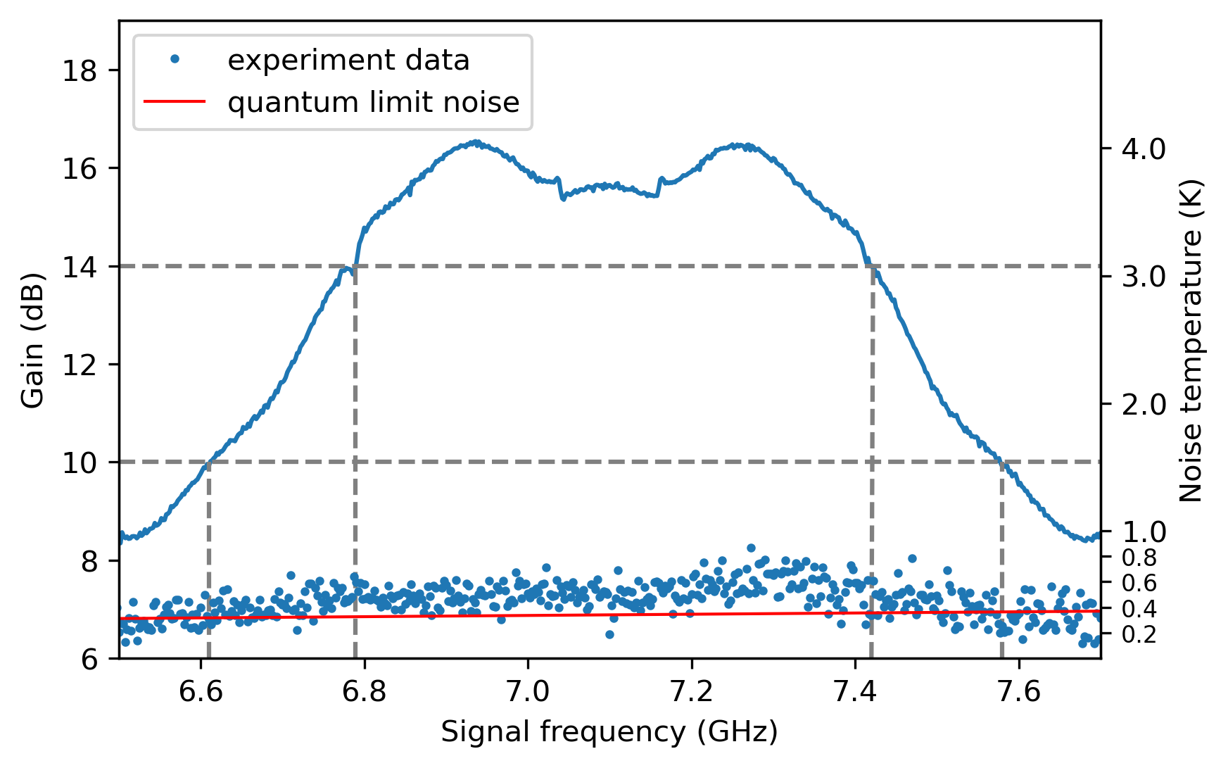
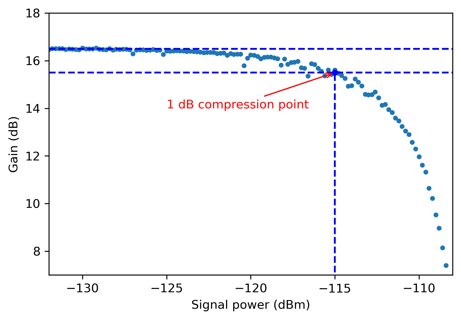
The initial step in characterizing our device is measuring the phase and amplitude components of parameter as a function of DC flux bias for various input signal frequency. Typically, the amplitude component of exhibits minimal variation with the DC bias due to the low quality factor, whereas the phase component of displays more pronounced changes. By varying the DC bias, we observe a periodic structure as illustrated in fig2a, which is attributed to the modulation of the critical current of the SQUID. Next, we determine the appropriate resonant frequency for signal amplification. We then measure the parameter with the IMPA pump on and off and define gain as . As shown in figure 2b, the measured gain exhibits a distinct bimodal frequency response. Specifically, the peak gain achieved is 16.5 dB. The bandwidth over which the gain exceeds 10 dB is measured to be approximately 1 GHz, while the bandwidth for which the gain remains above 14 dB is greater than 600 MHz. Figure 2b also shows the frequency-dependent behavior of noise, with the measured noise temperature of the IMPA closely approaching the quantum limit. Additionally, we investigate the gain as a function of input signal power, as illustrated in figure 2c, and find that the saturation power of the IMPA is -115 dBm.
We fabricate several IMPA devices with identical configurations, utilizing one of them to enhance the measurement quantum efficiency for photon quadrature measurement and tomography.Li et al. (2025) In the experiment, which involves the emission of on-demand shaped photons, we further assess the performance of IMPA. The Jaynes-Cummings (JC) model describes a system comprising a two-level atom (such as a superconducting qubit) coupled to a resonator. Denoting and as the frequencies of the qubit and the resonator, respectively, and as the qubit state operator, the Hamiltonian of the system is given by , where the frequency detuning significantly exceeds the coupling rate .Koch et al. (2007b) It becomes apparent that the state of the qubit dictates the frequency of the resonator. We then demodulate the signal into its in-phase (I) and quadrature (Q) components. Figure 3a and 3b display data acquired with the IMPA pump off and on, respectively. The blue and red points represent the readout states and . The single-shot measurements are repeated 3,000 times. Notably, with the IMPA activated, the state-discrimination visibility rises from 0.54 to 0.84 and the separation between the two clouds of data points becomes more distinct. This enhanced separation facilitates faster readout processesJeffrey et al. (2014) and improves the measurement fidelity.
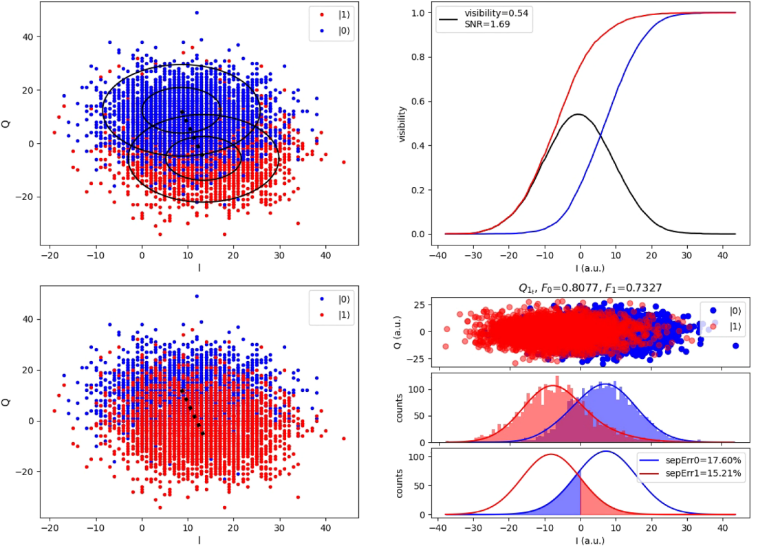
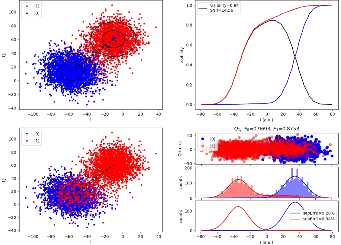
In the absence of IMPA pump and bias, we measure the relaxation time , the coherence time and the signal-to-noise ratio (SNR) to be 5.151 s, 3.007 s and 1.69, respectively. In contrast, when the IMPA pump and bias are applied, increases to 5.539 s, rises to 3.036 s and the SNR improves significantly to 14.56. These results demonstrate that the pump and bias of our IMPA significantly enhance the signal-to-noise ratio, while the impact of pump and bias on the decoherence properties of the qubits remains negligible. In the experimental setup for heterodyne measurement of quantum microwave field, we employ the IMPA to enhance SNR, thereby improving the stability of the quantum state tomography (QST) data. As a result, for the quantum state, the coefficient of variation of the QST data improves from 6.73% with IMPA off to 0.91% with IMPA on after repetitions. Moreover, after repetitions, the coefficient of variation of QST data improves from 3.22% with IMPA off to 0.19% with IMPA on. These results demonstrate the excellent performance in SNR enhancement in real experimental applications.
The overall quantum efficiency accounts for contributions from noise introduced by the amplifiers, losses and spurious reflections throughout the amplification chain, as well as inefficiencies during the detection process, which includes the sampling and data processing stages. Li et al. (2025) Given the significant gain of the IMPA, the system’s noise is primarily dominated by the noise introduced by the first near-quantum-limited amplifier. Blais et al. (2021) We calibrate the average photon number of the thermal noise induced by the amplification chain as , which yields an overall quantum efficiency of . This quantum efficiency surpasses the value reported by Ferreira et al. Ferreira et al. (2024) in a similar setup using a single Josephson traveling-wave parametric amplifier (JTWPA), where they measured . This comparison highlights the exceptional performance of the IMPA from a certain perspective.
We have fabricated and characterized several broadband impedance-transformed Josephson parametric amplifiers (IMPAs). One method has been introduced for preparing the capacitor’s dielectric layer, employing a double-layer lift-off process that offers improved stability and accelerates production compared with the traditional technique. Experimental results indicate that the IMPA achieves an instantaneous bandwidth over 950 (600) MHz with a gain exceeding 10 (14) dB, along with saturation input power of -115 dBm and near quantum-limited noise. Due to no significant degradation of the relaxation time and coherence time of the superconducting qubits, the backaction from the IMPA on qubits can be ingored. The IMPA significantly improves the SNR and enables the amplification chain to achieve a high quantum efficiency with , making it a critical necessity for large-scale quantum computation.
This work was supported by the National Natural Science Foundation of China (Grant Nos. 12204528, 92265207, T2121001, 92365301, T2322030, 12122504, 12274142, 12475017), the Innovation Program for Quantum Science and Technology (Grant No. 2021ZD0301800), the Beijing Nova Program (Grant No. 20220484121), the Natural Science Foundation of Guangdong Province (Grant No. 2024A1515010398). This work was supported by the Synergetic Extreme Condition User Facility (SECUF). Devices were made at the Nanofabrication Facilities at Institute of Physics, CAS in Beijing.
AUTHOR DECLARATIONS
Conflict of Interest
The authors have no conflicts to disclose.
Author Contributions
Zhengyang Mei and Xiaohui Song contributed equally to this work.
Zhengyang Mei: Conceptualization (equal); Data curation (equal); Formal analysis (equal); Investigation (lead); Methodology (supporting); Validation (equal); Visualization (lead); Writing – original draft (equal). Xiaohui Song: Conceptualization (equal); Data curation (equal); Formal analysis (equal); Investigation (supporting); Methodology (equal); Project administration (lead); Visualization (supporting); Writing – original draft (equal). Xueyi Guo: Data curation (supporting); Formal analysis (equal); Investigation (supporting); Software (lead). Xiang Li: Data curation (equal); Formal analysis (equal); Investigation (supporting); Software (supporting); Writing – original draft (supporting). Yunhao Shi: Software (supporting); Writing – original draft (supporting). Guihan Liang: Investigation (supporting). Chenglin Deng: Software (supporting). Li Li: Software (supporting). Yang He: Software (supporting). Dongning Zheng: Funding acquisition (equal); Project administration (supporting); Resources (supporting); Supervision(supporting); Writing – review & editing(supporting). Kai Xu: Funding acquisition (equal); Project administration (supporting); Resources (equal); Supervision(supporting); Writing – review & editing(supporting). Heng Fan: Funding acquisition (equal); Project administration (supporting); Resources (equal); Supervision(equal); Writing – review & editing(equal). Zhongcheng Xiang: Conceptualization (equal); Methodology (equal); Funding acquisition (equal); Project administration (supporting); Resources (equal); Supervision(equal); Writing – review & editing(equal).
DATA AVAILABILITY
The data that support the findings of this study are available from the corresponding authors upon reasonable request.
References
- Caves (1982) C. M. Caves, “Quantum limits on noise in linear amplifiers,” Phys. Rev. D 26, 1817–1839 (1982).
- Lin et al. (2013) Z. R. Lin, K. Inomata, W. D. Oliver, K. Koshino, Y. Nakamura, J. S. Tsai, and T. Yamamoto, “Single-shot readout of a superconducting flux qubit with a flux-driven josephson parametric amplifier,” Applied Physics Letters 103, 132602 (2013).
- Abdo et al. (2011) B. Abdo, F. Schackert, M. Hatridge, C. Rigetti, and M. Devoret, “Josephson amplifier for qubit readout,” Applied Physics Letters 99, 162506 (2011).
- Walter et al. (2017) T. Walter, P. Kurpiers, S. Gasparinetti, P. Magnard, A. Potočnik, Y. Salathé, M. Pechal, M. Mondal, M. Oppliger, C. Eichler, and A. Wallraff, “Rapid high-fidelity single-shot dispersive readout of superconducting qubits,” Phys. Rev. Appl. 7, 054020 (2017).
- Vijay et al. (2012) R. Vijay, C. Macklin, D. H. Slichter, S. J. Weber, K. W. Murch, R. Naik, A. N. Korotkov, and I. Siddiqi, “Stabilizing rabi oscillations in a superconducting qubit using quantum feedback,” Nature 490, 77–80 (2012).
- Ristè et al. (2013) D. Ristè, M. Dukalski, C. A. Watson, G. de Lange, M. J. Tiggelman, Y. M. Blanter, K. W. Lehnert, R. N. Schouten, and L. DiCarlo, “Deterministic entanglement of superconducting qubits by parity measurement and feedback,” Nature 502, 350–354 (2013).
- Yurke (1987) B. Yurke, “Squeezed-state generation using a josephson parametric amplifier,” J. Opt. Soc. Am. B 4, 1551–1557 (1987).
- Castellanos-Beltran et al. (2008) M. A. Castellanos-Beltran, K. D. Irwin, G. C. Hilton, L. R. Vale, and K. W. Lehnert, “Amplification and squeezing of quantum noise with a tunable josephson metamaterial,” Nature Physics 4, 929–931 (2008).
- Mooij et al. (1999) J. E. Mooij, T. P. Orlando, L. Levitov, L. Tian, C. H. van der Wal, and S. Lloyd, “Josephson persistent-current qubit,” Science 285, 1036–1039 (1999).
- You, Tsai, and Nori (2003) J. Q. You, J. S. Tsai, and F. Nori, “Controllable manipulation and entanglement of macroscopic quantum states in coupled charge qubits,” Phys. Rev. B 68, 024510 (2003).
- Koch et al. (2007a) J. Koch, T. M. Yu, J. Gambetta, A. A. Houck, D. I. Schuster, J. Majer, A. Blais, M. H. Devoret, S. M. Girvin, and R. J. Schoelkopf, “Charge-insensitive qubit design derived from the cooper pair box,” Phys. Rev. A 76, 042319 (2007a).
- Yamamoto et al. (2008) T. Yamamoto, K. Inomata, M. Watanabe, K. Matsuba, T. Miyazaki, W. D. Oliver, Y. Nakamura, and J. S. Tsai, “Flux-driven josephson parametric amplifier,” Applied Physics Letters 93, 042510 (2008).
- Reed et al. (2010) M. D. Reed, L. DiCarlo, B. R. Johnson, L. Sun, D. I. Schuster, L. Frunzio, and R. J. Schoelkopf, “High-fidelity readout in circuit quantum electrodynamics using the jaynes-cummings nonlinearity,” Phys. Rev. Lett. 105, 173601 (2010).
- Hatridge et al. (2011) M. Hatridge, R. Vijay, D. H. Slichter, J. Clarke, and I. Siddiqi, “Dispersive magnetometry with a quantum limited squid parametric amplifier,” Phys. Rev. B 83, 134501 (2011).
- Lucero et al. (2012) E. Lucero, R. Barends, Y. Chen, J. Kelly, M. Mariantoni, A. Megrant, P. O’Malley, D. Sank, A. Vainsencher, J. Wenner, T. White, Y. Yin, A. N. Cleland, and J. M. Martinis, “Computing prime factors with a josephson phase qubit quantum processor,” Nature Physics 8, 719–723 (2012).
- Barends et al. (2013) R. Barends, J. Kelly, A. Megrant, D. Sank, E. Jeffrey, Y. Chen, Y. Yin, B. Chiaro, J. Mutus, C. Neill, P. O’Malley, P. Roushan, J. Wenner, T. C. White, A. N. Cleland, and J. M. Martinis, “Coherent josephson qubit suitable for scalable quantum integrated circuits,” Phys. Rev. Lett. 111, 080502 (2013).
- Zhong et al. (2013) Y.-P. Zhong, C.-Y. Li, H.-H. Wang, and Y. Chen, “Progress in superconducting qubits from the perspective of coherence and readout,” Chinese Physics B 22, 110313 (2013).
- Chen et al. (2012) Y. Chen, D. Sank, P. O’Malley, T. White, R. Barends, B. Chiaro, J. Kelly, E. Lucero, M. Mariantoni, A. Megrant, C. Neill, A. Vainsencher, J. Wenner, Y. Yin, A. N. Cleland, and J. M. Martinis, “Multiplexed dispersive readout of superconducting phase qubits,” Applied Physics Letters 101, 182601 (2012).
- Fowler et al. (2012) A. G. Fowler, M. Mariantoni, J. M. Martinis, and A. N. Cleland, “Surface codes: Towards practical large-scale quantum computation,” Phys. Rev. A 86, 032324 (2012).
- Barends et al. (2014) R. Barends, J. Kelly, A. Megrant, A. Veitia, D. Sank, E. Jeffrey, T. C. White, J. Mutus, A. G. Fowler, B. Campbell, Y. Chen, Z. Chen, B. Chiaro, A. Dunsworth, C. Neill, P. O’Malley, P. Roushan, A. Vainsencher, J. Wenner, A. N. Korotkov, A. N. Cleland, and J. M. Martinis, “Superconducting quantum circuits at the surface code threshold for fault tolerance,” Nature 508, 500–503 (2014).
- Mutus et al. (2014) J. Y. Mutus, T. C. White, R. Barends, Y. Chen, Z. Chen, B. Chiaro, A. Dunsworth, E. Jeffrey, J. Kelly, A. Megrant, C. Neill, P. J. J. O’Malley, P. Roushan, D. Sank, A. Vainsencher, J. Wenner, K. M. Sundqvist, A. N. Cleland, and J. M. Martinis, “Strong environmental coupling in a josephson parametric amplifier,” Applied Physics Letters 104, 263513 (2014).
- Roy et al. (2015) T. Roy, S. Kundu, M. Chand, A. M. Vadiraj, A. Ranadive, N. Nehra, M. P. Patankar, J. Aumentado, A. A. Clerk, and R. Vijay, “Broadband parametric amplification with impedance engineering: Beyond the gain-bandwidth product,” Applied Physics Letters 107, 262601 (2015).
- Esposito et al. (2021) M. Esposito, A. Ranadive, L. Planat, and N. Roch, “Perspective on traveling wave microwave parametric amplifiers,” Applied Physics Letters 119, 120501 (2021).
- Macklin et al. (2015) C. Macklin, K. O’Brien, D. Hover, M. E. Schwartz, V. Bolkhovsky, X. Zhang, W. D. Oliver, and I. Siddiqi, “A near–quantum-limited josephson traveling-wave parametric amplifier,” Science 350, 307–310 (2015).
- Duan et al. (2021) P. Duan, Z. Jia, C. Zhang, L. Du, H. Tao, X. Yang, L. Guo, Y. Chen, H. Zhang, Z. Peng, W. Kong, H.-O. Li, G. Cao, and G.-P. Guo, “Broadband flux-pumped josephson parametric amplifier with an on-chip coplanar waveguide impedance transformer,” Applied Physics Express 14, 042011 (2021).
- Dolan (1977) G. J. Dolan, “Offset masks for lift-off photoprocessing,” Applied Physics Letters 31, 337–339 (1977).
- Song et al. (2021) P. Song, X. Guo, K. Xu, X. Song, Z. Wang, Z. Xiang, H. Li, L. Su, Y. Jin, and D. Zheng, “Fabrication of josephson parameter amplifier and its application in squeezing vacuum fluctuations,” Chinese Physics B 30, 128502 (2021).
- Li et al. (2025) X. Li, S.-Y. Li, S.-L. Zhao, Z.-Y. Mei, Y. He, C.-L. Deng, Y. Liu, Y.-J. Liu, G.-H. Liang, J.-Z. Wang, X.-H. Song, K. Xu, H. Fan, Y.-X. Zhang, Z.-C. Xiang, and D.-N. Zheng, “On-demand shaped-photon emission based on a parametrically modulated qubit,” Phys. Rev. Appl. 23, 024019 (2025).
- Koch et al. (2007b) J. Koch, T. M. Yu, J. Gambetta, A. A. Houck, D. I. Schuster, J. Majer, A. Blais, M. H. Devoret, S. M. Girvin, and R. J. Schoelkopf, “Charge-insensitive qubit design derived from the cooper pair box,” Phys. Rev. A 76, 042319 (2007b).
- Jeffrey et al. (2014) E. Jeffrey, D. Sank, J. Y. Mutus, T. C. White, J. Kelly, R. Barends, Y. Chen, Z. Chen, B. Chiaro, A. Dunsworth, A. Megrant, P. J. J. O’Malley, C. Neill, P. Roushan, A. Vainsencher, J. Wenner, A. N. Cleland, and J. M. Martinis, “Fast accurate state measurement with superconducting qubits,” Phys. Rev. Lett. 112, 190504 (2014).
- Blais et al. (2021) A. Blais, A. L. Grimsmo, S. M. Girvin, and A. Wallraff, “Circuit quantum electrodynamics,” Rev. Mod. Phys. 93, 025005 (2021).
- Ferreira et al. (2024) V. S. Ferreira, G. Kim, A. Butler, H. Pichler, and O. Painter, “Deterministic generation of multidimensional photonic cluster states with a single quantum emitter,” Nature Physics 20, 865–870 (2024).