Shift current response in twisted double bilayer graphenes
Abstract
We calculate the shift current response in twisted double bilayer graphenes (TDBG) by applying the perturbative approach to the effective continuum Hamiltonian. We have performed a systematic study of the shift current in AB-AB and AB-BA stacked TDBG, where we have investigated the dependence of the signal on the twist angle, the vertical bias voltage and the Fermi level. The numerical analyses demonstrate that a large signal is generated from the formation of the moiré minibands. Notably, we also found that there is a systematic sign reversal of the signal in the two stacking configurations below the charge neutrality point for large bias voltages. We qualitatively explain the origin of this sign reversal by studying the shift current response in AB-stacked bilayer graphene.
I Introduction
The study of moiré systems has been one of the major focusses of modern condensed matter physics. By stacking two sheets with a relative twist angle, the total system shows a moiré pattern originating from the lattice mismatch between the two layers. This moiré pattern leads to a modification of the band structure of the system, where the most notable example is the flat band formation and the experimental observation of superconductivity in twisted bilayer graphene (TBG) at an angle known as the magic angle [1; 2; 3]. Studies has expanded to other graphene-based moiré systems, such as twisted monolayer-bilayer [4; 5; 6; 7; 8; 9; 10; 11; 12; 13], twisted trilayer [14; 15; 16; 17; 18; 19; 20], and other twisted multilayer graphene [21; 22; 23; 24].
Twisted double bilayer graphene (TDBG) is a moiré system where two sheets of AB-stacked bilayer graphene (BLG) are stacked with a relative twist angle, as shown in Fig. 1. A variety of studies on TDBG has been performed, such as the observation of strongly correlated phenomena [25; 26; 27; 28; 29; 30; 31; 32; 33; 34; 35; 36; 37; 38; 39; 40], owing to its highly tuneable band structure, where a band gap can be opened through the application of a vertical bias voltage. Importantly, TDBG can be fabricated in two distinct stacking structures, known as AB-AB and AB-BA, respectively shown in Fig. 1 (a) and (b). The AB-AB stacking is composed of two bilayer sheets stacked and twisted with the same orientation, while the AB-BA stacking introduces a offset on the second layer. A schematic diagram of the respective variants are shown in Fig. 1 (a) and (b). It is known that the two variants have completely different valley Chern numbers while hosting very similar band structures [25; 26; 21].
Simultaneously, the shift current response has been under intense investigation due to its potential to probe the topology, quantum geometry and the symmetry of a variety of materials [41; 42; 43; 44; 45; 46; 47]. This is a second order nonlinear optical response where light is rectified into dc current in noncentrosymmetric materials [48; 49; 50]. It is characterised by a quantity known as the shift vector, which is expressed in terms of the difference between the Berry connection of the initial and final band of the optical excitation. The shift current response has been experimentally measured in various 2D materials [43; 51; 52; 53; 54; 55; 56; 57; 58], where the two main types which have been actively studied are the family of transition metal dichalcogenides [59; 60; 61; 62; 63; 64; 65; 66; 67; 68; 69] and ferroelectric 2D materials, such as transition metal monochalcogenides [70; 52; 55] and CuInP2S6 [71; 54].
Nowadays, the scope of investigation of the shift current has expanded to moiré materials [72; 31; 73; 74; 38; 75; 76] where there is no need to rely on the polarisation of the monolayer to observe a finite shift current; for example, two non-polar materials with a lattice mismatch can be stacked in order to create an interface with broken inversion symmetry. The shift current response in TBG, being one of the simplest moiré system, has been studied theoretically [31; 73; 77; 78]. However, the symmetry renders the in-plane shift current to vanish [78], thus, an extra term is required in the TBG Hamiltonian to break such symmetry. This is achieved by introducing an asymmetric potential between the A and B sites which can be experimentally realised through the alignment with hBN. There have also been studies of the shift current in other graphitic systems [31; 38; 74] and heterostrucutres [63; 72; 53], such as WSe2/black phosphorene heterostructure [53] and twisted TMD heterobilayers [72; 79].
In the present work, we theoretically study the shift current response in AB-AB and AB-BA stacked TDBG. This is motivated by the fact that TDBG is composed of AB-stacked BLG, which has broken symmetry, allowing for a finite in-plane shift current response without the need for any substrate or external field unlike TBG. Furthermore, the band structure of TDBG is highly tuneable through the application of a vertical bias voltage, giving an extra degree of freedom to investigate the behaviour of the shift current. The fact that the two variants of TDBG exhibit similar band structures with distinct topologies [25; 26; 21] offers a platform to study how this contrast influences the shift current response. One previous work has studied the shift current response in AB-AB and AB-BA stacked TDBG for fixed values of the twist angle, Fermi level and vertical bias voltage [31], however, the relationship between the two variants was unclear. Here, we systematically investigate the twist angle, Fermi level and vertical bias voltage dependence on the TDBG shift current to study its relation to the stacking configuration. In particular, we have found a systematic sign reversal in the signals of the AB-AB and AB-BA variants when a large vertical bias voltage is applied. We further give a qualitative explanation on the origin of this sign reversal by studying the shift current in AB-stacked BLG.
The present paper is organised as follows. In Section II, we introduce the effective continuum Hamiltonian for TDBG and the theoretical expression of the shift current. Then, in Section III, we present our results of the shift current response in TDBG and provide a discussion on the interpretation on the results in Section IV. Finally, we will conclude the present paper in Section V.
II Model and Methods
II.1 Twisted double bilayer graphene
The primitive lattice vectors of the graphene lattice are chosen to be and , where 0.246nm is the lattice constant. Then, the corresponding reciprocal lattice vectors are and . AB-stacked bilayer graphene (BLG), which can be prepared by stacking two graphene sheets with the A and B sites of the upper and lower layers aligned, shares the same primitive lattice vectors with monolayer graphene, thus, the Brillouin zones are also common. A schematic diagram is shown on the left side of Fig. 1 (a), where there are four atomic sites labelled , , and . Sites (), which are vertically aligned, are referred to as the dimerised sites and experience an energy offset of 0.050 eV.
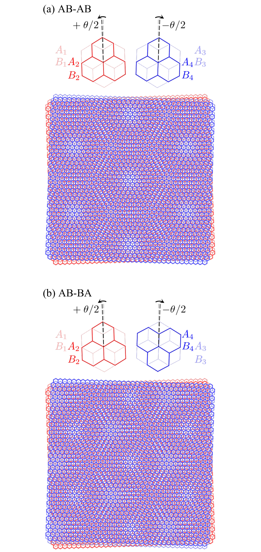
Twisted double bilayer graphene (TDBG) is a system where two sheets of AB-stacked BLG are stacked and twisted with a relative twist angle, as shown in Fig. 1 (a), (b). To fabricate a sample of TDBG, we first stack the two BLG without twisting. There are two ways to perform this operation: one is to simply stack the two BLG sheets with the same orientation and the other is to perform a rotation about the -axis on one sheet and then stacking the two. Then, a relative twist angle between the two BLG sheets is introduced to form a sample of TDBG. Here, the first variant is known as AB-AB stacking, while the second is known as AB-BA stacking. Their respective structures are shown in Fig. 1 (a) and (b), and the difference in their moiré patterns can be seen. Hence, the extra rotation leads to a different environment at the twist interface between the two stacking configurations, resulting in different band topologies [25]. It should also be noted that the AB-AB variant has the in-plane three-fold rotational symmetry inherited from monolayer graphene and a two-fold rotational symmetry along along the -axis. Similarly, the AB-BA variant has and rotational symmetries.
In cases when the moiré lattice constant is much greater than the graphene lattice constant, i.e. when the twist angle is small, we can construct an effective continuum Hamiltonian for TDBG around the valleys. When the lower layer () and the upper layer () are rotated by an angle , the reciprocal lattice vectors in the respective layers are given as , where is the two dimensional rotation matrix. This allows us to define the moiré reciprocal lattice vectors .
The Hamiltonians for AB-AB and AB-BA TDBG are written as
| (1) | ||||
where we have defined
| (2) | ||||
The velocities are defined as , being hopping integrals, and , being the valley index . Namely, eV is the intralayer nearest neighbouring hopping, 0.4 eV is the hopping between the dimerised sites, 0.32 eV and 0.044 eV are the diagonal hopping between the (, ) and (, ) sites, respectively. Also, and are the valleys in the respective layers. By inspecting the Hamiltoanians, we can see that the top left block corresponds to the Hamiltonian for AB-stacked BLG. We have the same Hamiltonian in the bottom right block for , however, for , we can see that the pairs and are interchanged, reflecting the difference in stacking configuration. The interlayer moiré potential is given by
| (3) | ||||
where 0.0797 eV, 0.0975 eV [25; 80] and is the cube root of unity. The final term is the diagonal matrix modelling the vertical bias voltage
| (4) |
We note that a finite breaks the / rotational symmetries in the AB-AB/AB-BA stacked TDBG. In this system, the twist angle and the vertical bias voltage are the parameters that can be modified experimentally.
The numerical evaluation of Hamiltonians in Eq. (1) involves expanding in term of the Fourier components with respect to , with integers and . This Fourier expansion entails the introduction of a cutoff in space, and in this study, we have adopted a cutoff of .
II.2 Shift current
When two rays of light, and polarised in the direction with frequency respectively, are shone to a sample, we expect a current density in the direction resulting from a second order nonlinear optical (NLO) response. Here, in the present 2D set-up. Adopting the Einstein summation convention over repeated indices, the second order NLO response is expressed as
| (5) |
where is the second order NLO conductivity tensor and . It should be noted that will be finite only when the system lacks inversion symmetry [48; 49], which can be checked by inspecting the inversion symmetry of both sides of Eq. (5).
The shift current corresponds to the case where , resulting in a dc response . If we choose to focus on the case where the incoming light is of a single polarisation , the shift current conductivity in 2D is given by the following expression [49; 50]
| (6) |
Here, is the charge of the carrier, , where is the eigenenergy of the Bloch state , , where is the Fermi-Dirac occupation function, is the velocity operator, where is used as a shorthand for . We also introduce the shift vector , defined using the intraband Berry connection and the phase of the velocity matrix element .
A close inspection of Eq. (6) allows us to deduce a couple of key features of the shift current. First, is the joint density of states (JDoS) which counts the number of states that are separated by energy , and is the dipole matrix element which dictates the transition rules at each -point. Thus, we can conclude that and respectively labels the initial and final state of the optical transition and that the magnitude of the current is proportional to the number of states available for the transition. Second, the shift current is characterised by the shift vector . It is expressed as the difference between the intraband Berry connections of the initial and final bands of the optical transition, and we can understand this as being the difference in the centre-of-mass coordinate of the electron wavepacket in the initial and the final band [81; 82; 83]. The final term is present to ensure that is gauge invariant.
In the present paper, we only work with Hamiltonians which are linear in . This allows us to rewrite Eq. (6) as [73]
| (7) |
where we have set , where is the elemental charge. Here, we can view the states and as the initial and final states of the real optical transition, while state corresponds to some intermediate state that is reached through virtual transitions. The numerical evaluation of the shift current response in the present work was performed using this expression. We replace the integral over the moiré Brillouin zone by a summation over a mesh of and employ a Lorentzian function with a broadening 1 meV in place of .
In applying Eq. (7) to our system, we can perform a simple symmetry analysis on the tensor to find its independent components. To do so, we return to Eq. (5) and consider a transformation from coordinates to a new set of coordinates given by a rotation matrix . In this new frame, we can rewrite Eq. (5) as
| (8) |
leading us to the following transformation law
| (9) |
Imposing symmetry, in which we set with , we find [31]
| (10) | ||||
Therefore, only contains two independent components, and . Since any signal can be expressed in terms of and , in the subsequent sections, we solely focus on these two components. We further note that in the case where the vertical bias voltage is absent, AB-AB (AB-BA) configuration recovers the () rotational symmetry [25], further rendering = 0 ( = 0).
III Results
III.1 Intrinsic shift current response
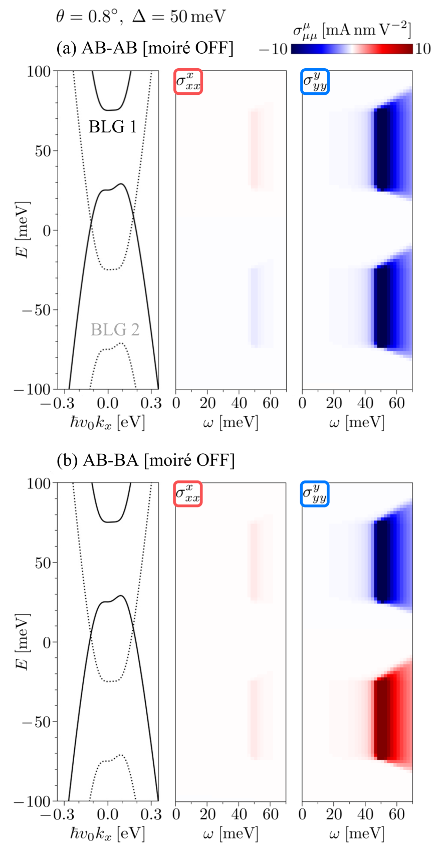
We compute the shift current response in twisted double bilayer graphene (TDBG) at a twist angle of . We specifically focus on the intrinsic signal in the absence of any bias voltage 0.
The results for the response in AB-AB and AB-BA stacked TDBG are shown on the leftmost panels in Fig. 2 (a) and (b) respectively. Focussing on the AB-AB variant, we show the band structure on the left panel and as a colour density plot on the right panel. The shift current is plotted with frequency meV on the horizontal and Fermi level meV on the vertical axis. Therefore, each horizontal strip of the density plot corresponds to a - plot for a certain value of . We note that the scale of the vertical axis is adjusted to match that of the band structure plot. In Fig. 2 (b), we show the corresponding plots for AB-BA TDBG, however, due the the symmetry, is completely suppressed.
If we inspect the density plot in AB-AB TDBG, we see that there is a strong signal in the low frequency region which gradually tails off as we move to higher frequencies. This behaviour is seen throughout the plotted range and is due to the prefactor in Eq. (6). This prefactor acts to enhance the signal when the gap is small and to cause a suppression for high frequencies. The enhancement is especially strong near the charge neutrality point (CNP), indicated by the grey arrow, where bands are concentrated giving rise to very small energy gaps. A similar enhancement of the shift current is reported other moiré materials [31; 72; 73; 74]. We also notice that the low frequency signal is not of a single sign but a series of sign changes is observed as the Fermi level is swept. Note that the signal should technically vanish as , however, due to to the finite broadening and the colour scale of the density plot, it appears that there is a finite response in the dc limit.
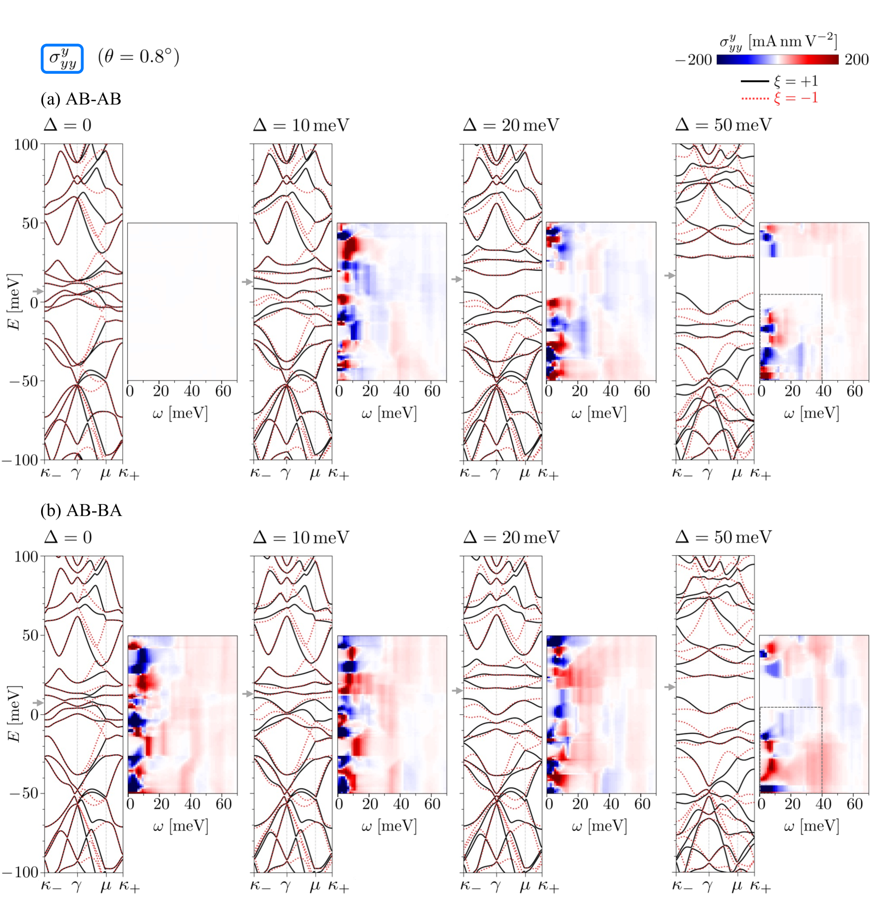
The results for the response are shown in Fig. 3 in a similar fashion. In this case, the (b) AB-BA variant gives a finite response while it vanishes in the (a) AB-AB case due to the symmetry. Although there are differences between the and responses, we find that their overall behaviour, such as the strong enhancement at low frequencies, are common.
III.2 Effect of vertical bias voltage
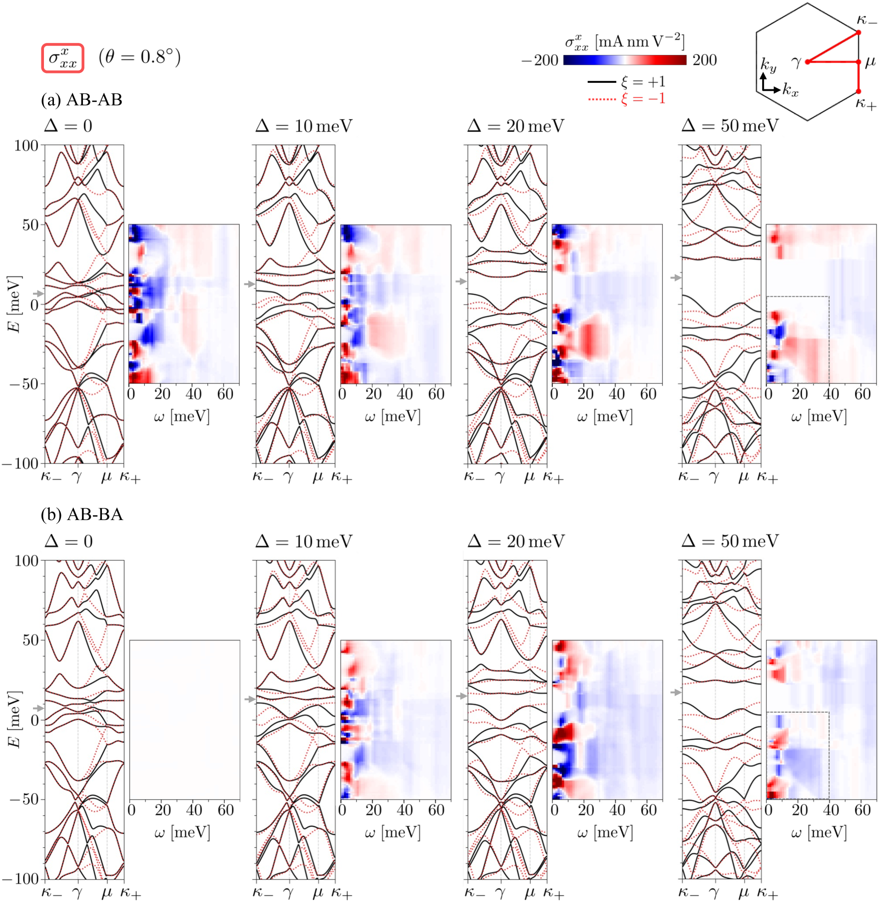
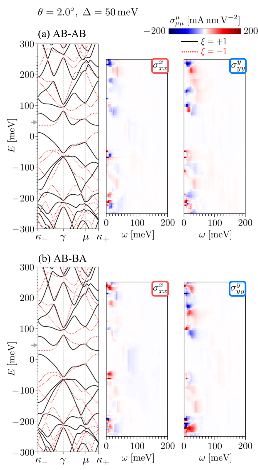
Having studied the behaviour of the intrinsic shift current response, we now move our attention to the evolution of the response as a result of the application of . We begin with the response at values of 10, 20 and 50 meV and show the band structures of AB-AB and AB-BA stacked TDBG in Fig. 2 (a) and (b) respectively.
Focussing on the AB-AB configuration, where is always non-zero, as is increased, we see that the overall size of the signal is suppressed. This is due to the fact that the bias voltage increases the gap size, which in turn suppresses the signal via the factor. On the other hand, in the AB-BA variant, as soon as the vertical bias voltage begins to break the symmetry, we observe a finite response. From here, the signal continues to grow in magnitude until 10 meV, from which the signal follows the same pattern with the suppression for stronger . A similar pattern between the signal strength and the band gap can be seen when the twist angle is increased. The results for and at 50 meV are given in Appendix A.
We further notice that there is a large insulating region, represented in white, near the CNP as increases. This behaviour can be simply inferred from the large band gap that opens at the CNP. We see similar trends in the response show in in Fig. 3 (a) and (b).
III.3 Comparison between AB-AB and AB-BA stacked TDBG
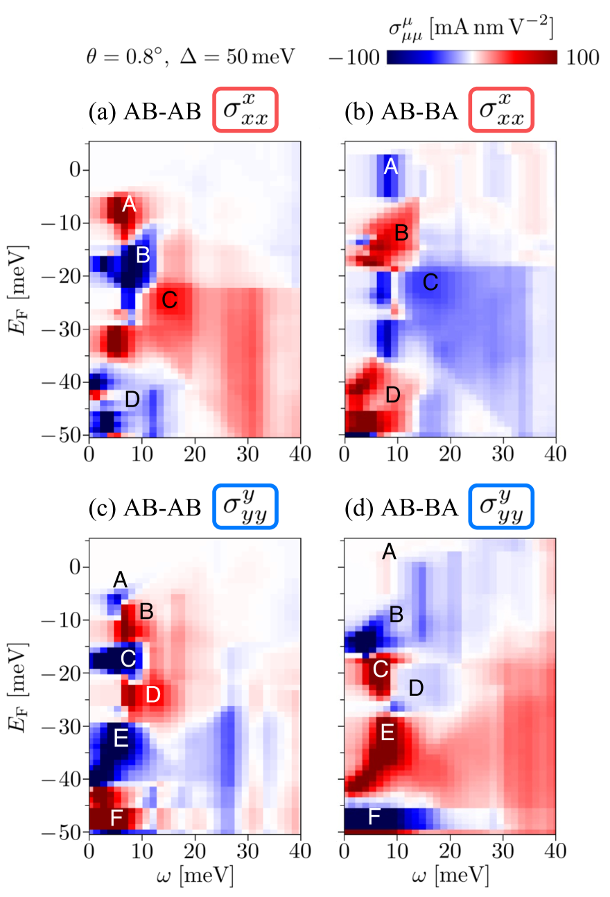
We find that there is a visible relationship between the signals of the two variants when is large and the bands are well separated. To allow for a systematic comparison of the shift current response between the two stacking configurations, we consider the case where a finite vertical bias voltage of 50 meV is applied. On the rightmost side of Fig. 2, we show the band structure and the corresponding plots for (a) AB-AB and (b) AB-BA stacked TDBG.
If we begin to compare the density plots between the two stacking configurations, we notice that there is a general positive/negative correlation in the sign of the signal above/below the CNP. The negative correlation is illustrated in Fig. 4 where we show a close-up view of the four density plots below the CNP, indicated by the grey dashed boxes in Fig. 2 and 3. Focussing first on the response shown in Fig. 4 (a) and (b), we have labelled four regions from A to D where a sign reversal can be seen. For example, in the AB-AB variant, region A has a positive signal, while the corresponding signal in the AB-BA variant is negative. A similar pattern is seen for the other three regions. Likewise, in Fig. 4 (c) and (d), where show the density plots for , we find that regions with the same label have opposite signs. We note that this positive/negative correlation is overshadowed as we turn down and the bands begin to cluster.
IV Understanding sign reversal in TDBG shift current
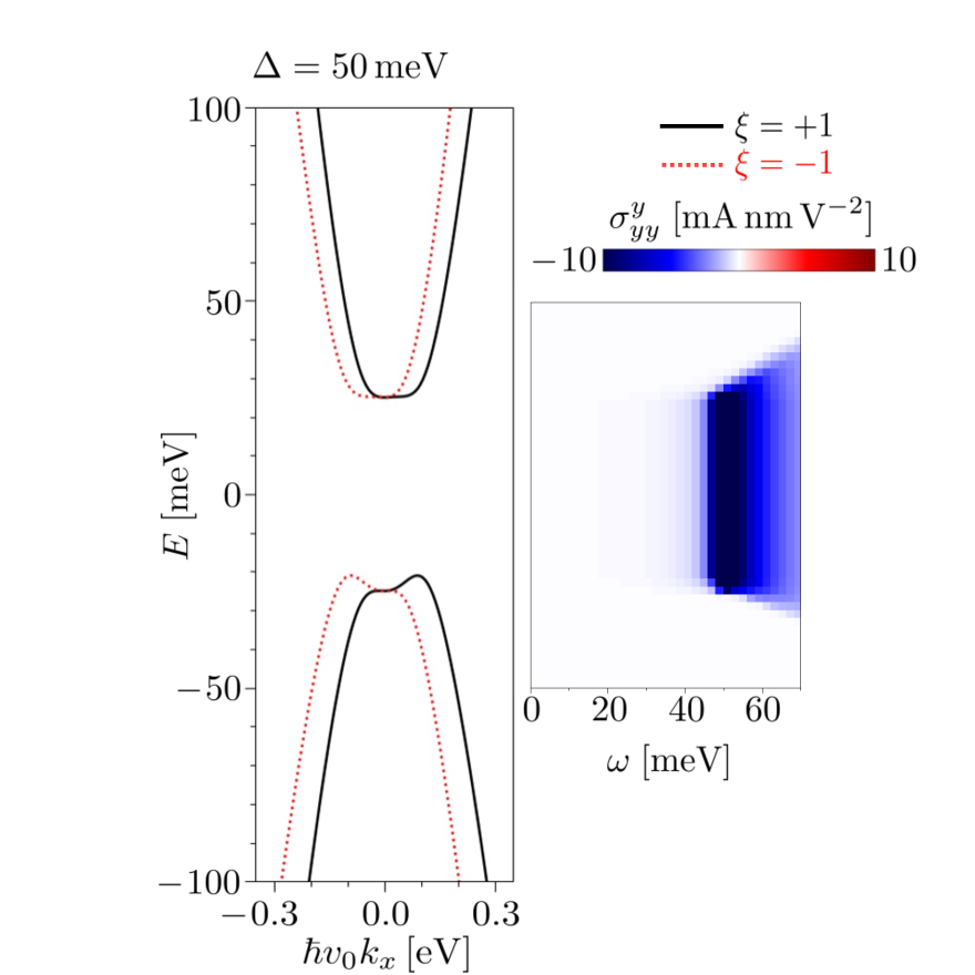
In order to understand the sign reversal seen in the AB-AB and AB-BA stacked TDBG, we consider the shift current response in AB-stacked bilayer graphene (BLG). We note that BLG is intrinsically centrosymmetric, hence, requires some external symmetry breaking for a finite response. In the present case, we apply a vertical bias voltage of 50 meV to match the value of in the previous section. It should also be noted that BLG has mirror symmetry across the - plane, which renders to zero. Therefore, it will suffice to study to describe its shift current response.
The continuum Hamiltonian for BLG around the valleys is given by the top left matrix in Eq. (1),
| (11) |
where represents the vertical bias voltage
| (12) |
Using this Hamiltonian, we show the band structure (left panel) and the corresponding response (right panel) of BLG in Fig. 5. The band structure computed from the Hamiltonian in Eq. (11) shows a slice through at around the () point, plotted in the black solid (red dashed) line. The vertical bias voltage allows for a gap-opening of around 50 meV. On the right panel, we show the shift current response as a colour density plot with frequency on the horizontal and Fermi level on the vertical axis. The numerical evaluation of Eq. (7) was performed with a broadening of 1 meV. We can initially see that there is very little or no response at frequencies below 50 meV, which is a reflection of the fact that there are no possible optical transitions in this frequency range due to the gap opened via the bias voltage. As we move up to 50 meV, we start to see a large response when the Fermi level is set within the gap. This sharp response corresponds to the optical transition from the band edge of the valence to that of the conduction band, where a large joint density of states (JDoS) is realised. We also note that the size of the signal is in the range of 10 mA nm , which is an order of magnitude smaller compared to the signal seen in TDBG. This result suggests that the effect of the moiré reconstruction of the band structure indeed enhances the shift current response.
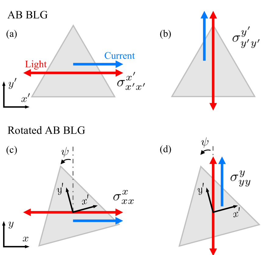
We next move on to the case where two AB-stacked BLG are stacked and twisted with no coupling at the twist interface, which we will refer to as uncoupled TDBG. Since the two sheets of BLG are uncoupled, the shift current response of the total system is given by the sum of the responses from each BLG.
The results of the shift current shown in Fig. 5 are given with respect to coordinates aligned with the lattice orientation of the BLG, which we will denote using primed coordinates . However, once we begin to rotate the BLG sheets, we are in need to compute the components of the shift current, and , with respect to the fixed coordinates denoted by unprimed coordinates. A schematic diagram of the set-up under consideration is shown in Fig. 6. Using the transformation law in Eq. (9), the relationship between the conductivities are given as
| (13) | ||||
where we have used the fact that . The detail of the derivation is described in Appendix. B. We note that, now, both and are finite since symmetry is broken as the two BLG sheets are twisted relative to each other.
Now, that we have an expression for and , we will apply this to the uncoupled TDBG. Here, we use the parameters and 50 meV. In Fig. 7, we show the schematic band structures of (a) AB-AB and (b) AB-BA uncoupled TDBG at the point, which simply corresponds to having two copies of the band structure shown in Fig. 5 with a shift in the Fermi energy. On the right panels, we show the density plots for the shift current conductivities and . Fist, we note that the magnitudes of is much smaller than , which stems from the fact that grows linearly with for small twist angles.
If we focus on the signs of the signal on the centre panels, we can see that there is a positive/negative correlation above/below the charge neutrality point between the two variants. This can be understood from the fact that the relative orientation of the BLG sheets are aligned/antialigned in the AB-AB/AB-BA variant. As the shift current is related to the polarisation of the material, the rotation of the second layer leads to a sign reversal of the signal. The same effect is seen in the signal on the right panels. This qualitatively explains the sign reversal that was seen in the TDBG calculation, and it reveals that this relationship is retained even after the effect of the moiré coupling.
V Conclusion
In the present paper, we have studied the shift current response in AB-AB and AB-BA stacked twisted double bilayer graphene (TDBG). We have studied the intrinsic signal and the effect on the signal as we turn on the vertical bias voltage and their dependence on the Fermi level. In the low frequency regime, we have found a strong signal and a series of sign flips across band edges. We have further found a positive/negative correlation in the sign of the signal between the AB-AB and AB-BA variants above/below the charge neutrality point at large values of the vertical bias voltage. To understand the origin of the sign relationship between the two variants, we used a simplified model for TDBG with no moiré coupling at the twist interface. By studying the response in this system, we have found that the sign reversal originated from the rotation of one of the bilayer and that the relative sign between the variants is retained even after the effects of the moiré reconstruction of the bands.
Acknowledgements.
This work was supported by JSPS KAKENHI Grants No. JP20K14415, No. JP20H01840, No. JP20H00127, No. JP21H05236, No. JP21H05232, JP24K06921, by JST CREST Grant No. JPMJCR20T3, and by JST SPRING, Grant No. JPMJSP2138, Japan.Appendix A Results for and
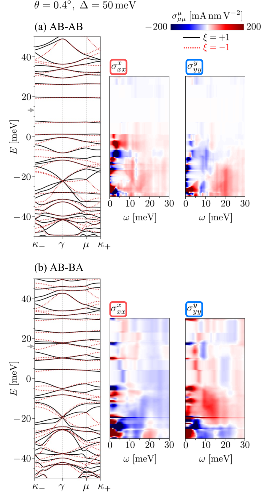
Here, we show the band structures and shift current plots for AB-AB and AB-BA TDBG for and with 50 meV. The results for and are shown in Fig. 8 and Fig. 9, respectively. We can see that the signal strength is strong at , while it is suppressed at . This is a similar behaviour to what was seen when the vertical bias voltage was increased, in which, the widened band gap suppressed the signal strength via the factor. We further note that the sign reversal that was seen below the charge neutrality point in the , 50 meV) case is overshadowed at , which is mainly due to the fact that the bands are much more dispersive compared to the case.
Appendix B Transformation of the conductivity tensor in non-moiré TDBG
In this appendix, we show the detail of the calculation that was performed to obtain Eq. (13). Using the explicit forms for the rotation matrix
| (14) |
and the conductivity tensor in the coordinates aligned with the BLG lattice
| (15) |
we can perform the matrix multiplication in Eq. (13) to obtain the tensor in the unprimed coordinates. It reads
| (16) |
where the matrix is explicitly given as
| (17) |
Then, the and components are given as
| (18) | ||||
Recalling that from the mirror symmetry, we finally end with
| (19) | ||||
which is the expression we have used in Section IV.
References
- Bistritzer and MacDonald [2011] R. Bistritzer and A. H. MacDonald, Proceedings of the National Academy of Sciences 108, 12233 (2011).
- Cao et al. [2018a] Y. Cao, V. Fatemi, S. Fang, K. Watanabe, T. Taniguchi, E. Kaxiras, and P. Jarillo-Herrero, Nature 556, 43 (2018a).
- Cao et al. [2018b] Y. Cao, V. Fatemi, A. Demir, S. Fang, S. L. Tomarken, J. Y. Luo, J. D. Sanchez-Yamagishi, K. Watanabe, T. Taniguchi, E. Kaxiras, et al., Nature 556, 80 (2018b).
- Rademaker et al. [2020] L. Rademaker, I. V. Protopopov, and D. A. Abanin, Physical Review Research 2, 033150 (2020).
- Park et al. [2020] Y. Park, B. L. Chittari, and J. Jung, Physical Review B 102, 035411 (2020).
- He et al. [2021a] M. He, Y.-H. Zhang, Y. Li, Z. Fei, K. Watanabe, T. Taniguchi, X. Xu, and M. Yankowitz, Nature Communications 12, 4727 (2021a).
- Xu et al. [2021] S. Xu, M. M. Al Ezzi, N. Balakrishnan, A. Garcia-Ruiz, B. Tsim, C. Mullan, J. Barrier, N. Xin, B. A. Piot, T. Taniguchi, et al., Nature Physics 17, 619 (2021).
- Chen et al. [2021] S. Chen, M. He, Y.-H. Zhang, V. Hsieh, Z. Fei, K. Watanabe, T. Taniguchi, D. H. Cobden, X. Xu, C. R. Dean, et al., Nature Physics 17, 374 (2021).
- Li et al. [2022a] S.-y. Li, Z. Wang, Y. Xue, Y. Wang, S. Zhang, J. Liu, Z. Zhu, K. Watanabe, T. Taniguchi, H.-j. Gao, et al., Nature communications 13, 4225 (2022a).
- Tong et al. [2022] L.-H. Tong, Q. Tong, L.-Z. Yang, Y.-Y. Zhou, Q. Wu, Y. Tian, L. Zhang, L. Zhang, Z. Qin, and L.-J. Yin, Physical Review Letters 128, 126401 (2022).
- Li et al. [2022b] S.-y. Li, Z. Wang, Y. Xue, Y. Wang, S. Zhang, J. Liu, Z. Zhu, K. Watanabe, T. Taniguchi, H.-j. Gao, et al., Nature communications 13, 4225 (2022b).
- Boschi et al. [2024] A. Boschi, Z. M. Gebeyehu, S. Slizovskiy, V. Mišeikis, S. Forti, A. Rossi, K. Watanabe, T. Taniguchi, F. Beltram, V. I. Fal’ko, et al., Communications Physics 7, 391 (2024).
- Zhang et al. [2024] H. Zhang, Q. Li, Y. Park, Y. Jia, W. Chen, J. Li, Q. Liu, C. Bao, N. Leconte, S. Zhou, et al., Nature Communications 15, 3737 (2024).
- Zhu et al. [2020] Z. Zhu, S. Carr, D. Massatt, M. Luskin, and E. Kaxiras, Physical review letters 125, 116404 (2020).
- Park et al. [2021] J. M. Park, Y. Cao, K. Watanabe, T. Taniguchi, and P. Jarillo-Herrero, Nature 590, 249 (2021).
- Ma et al. [2021] Z. Ma, S. Li, Y.-W. Zheng, M.-M. Xiao, H. Jiang, J.-H. Gao, and X. Xie, Science Bulletin 66, 18 (2021).
- Hao et al. [2021] Z. Hao, A. Zimmerman, P. Ledwith, E. Khalaf, D. H. Najafabadi, K. Watanabe, T. Taniguchi, A. Vishwanath, and P. Kim, Science 371, 1133 (2021).
- Phong et al. [2021] V. T. Phong, P. A. Pantaleón, T. Cea, and F. Guinea, Physical Review B 104, L121116 (2021).
- Kim et al. [2022a] H. Kim, Y. Choi, C. Lewandowski, A. Thomson, Y. Zhang, R. Polski, K. Watanabe, T. Taniguchi, J. Alicea, and S. Nadj-Perge, Nature 606, 494 (2022a).
- Turkel et al. [2022] S. Turkel, J. Swann, Z. Zhu, M. Christos, K. Watanabe, T. Taniguchi, S. Sachdev, M. S. Scheurer, E. Kaxiras, C. R. Dean, et al., Science 376, 193 (2022).
- Liu et al. [2019] J. Liu, Z. Ma, J. Gao, and X. Dai, Physical Review X 9, 031021 (2019).
- Park et al. [2022] J. M. Park, Y. Cao, L.-Q. Xia, S. Sun, K. Watanabe, T. Taniguchi, and P. Jarillo-Herrero, Nature Materials 21, 877 (2022).
- Nguyen et al. [2022] V. H. Nguyen, T. X. Hoang, and J.-C. Charlier, Journal of Physics: Materials 5, 034003 (2022).
- Shin et al. [2023] K. Shin, Y. Jang, J. Shin, J. Jung, and H. Min, Physical Review B 107, 245139 (2023).
- Koshino [2019] M. Koshino, Phys. Rev. B 99, 235406 (2019).
- Chebrolu et al. [2019] N. R. Chebrolu, B. L. Chittari, and J. Jung, Phys. Rev. B 99, 235417 (2019).
- Burg et al. [2019] G. W. Burg, J. Zhu, T. Taniguchi, K. Watanabe, A. H. MacDonald, and E. Tutuc, Physical review letters 123, 197702 (2019).
- Crosse et al. [2020] J. A. Crosse, N. Nakatsuji, M. Koshino, and P. Moon, Phys. Rev. B 102, 035421 (2020).
- Liu et al. [2020] X. Liu, Z. Hao, E. Khalaf, J. Y. Lee, Y. Ronen, H. Yoo, D. Haei Najafabadi, K. Watanabe, T. Taniguchi, A. Vishwanath, et al., Nature 583, 221 (2020).
- Haddadi et al. [2020] F. Haddadi, Q. Wu, A. J. Kruchkov, and O. V. Yazyev, Nano letters 20, 2410 (2020).
- Liu and Dai [2020] J. Liu and X. Dai, npj Computational Materials 6, 57 (2020).
- Culchac et al. [2020] F. J. Culchac, R. Del Grande, R. B. Capaz, L. Chico, and E. S. Morell, Nanoscale 12, 5014 (2020).
- Shen et al. [2020] C. Shen, Y. Chu, Q. Wu, N. Li, S. Wang, Y. Zhao, J. Tang, J. Liu, J. Tian, K. Watanabe, et al., Nature Physics 16, 520 (2020).
- Cao et al. [2020] Y. Cao, D. Rodan-Legrain, O. Rubies-Bigorda, J. M. Park, K. Watanabe, T. Taniguchi, and P. Jarillo-Herrero, Nature 583, 215 (2020).
- He et al. [2021b] M. He, Y. Li, J. Cai, Y. Liu, K. Watanabe, T. Taniguchi, X. Xu, and M. Yankowitz, Nature Physics 17, 26 (2021b).
- Szentpéteri et al. [2021] B. Szentpéteri, P. Rickhaus, F. K. de Vries, A. Márffy, B. Fulop, E. Tóvári, K. Watanabe, T. Taniguchi, A. Kormányos, S. Csonka, et al., Nano Letters 21, 8777 (2021).
- Wang et al. [2022] Y. Wang, J. Herzog-Arbeitman, G. W. Burg, J. Zhu, K. Watanabe, T. Taniguchi, A. H. MacDonald, B. A. Bernevig, and E. Tutuc, Nature Physics 18, 48 (2022).
- Ma et al. [2022] C. Ma, S. Yuan, P. Cheung, K. Watanabe, T. Taniguchi, F. Zhang, and F. Xia, Nature 604, 266 (2022).
- Rubio-Verdú et al. [2022] C. Rubio-Verdú, S. Turkel, Y. Song, L. Klebl, R. Samajdar, M. S. Scheurer, J. W. Venderbos, K. Watanabe, T. Taniguchi, H. Ochoa, et al., Nature Physics 18, 196 (2022).
- Tomić et al. [2022] P. Tomić, P. Rickhaus, A. Garcia-Ruiz, G. Zheng, E. Portolés, V. Fal’ko, K. Watanabe, T. Taniguchi, K. Ensslin, T. Ihn, et al., Physical Review Letters 128, 057702 (2022).
- Tan et al. [2016] L. Z. Tan, F. Zheng, S. M. Young, F. Wang, S. Liu, and A. M. Rappe, npj Computational Materials 2, 16026 (2016).
- Orenstein et al. [2021] J. Orenstein, J. Moore, T. Morimoto, D. Torchinsky, J. Harter, and D. Hsieh, Annual Review of Condensed Matter Physics 12, 247 (2021).
- Aftab et al. [2022] S. Aftab, M. Z. Iqbal, Z. Haider, M. W. Iqbal, G. Nazir, and M. A. Shehzad, Advanced Optical Materials 10, 2201288 (2022).
- Ma et al. [2023] Q. Ma, R. Krishna Kumar, S. Y. Xu, F. H. L. Koppens, and J. C. W. Song, Nature Reviews Physics 5, 170 (2023).
- Ahn et al. [2022] J. Ahn, G.-Y. Guo, N. Nagaosa, and A. Vishwanath, Nature Physics 18, 290 (2022).
- Cook et al. [2017] A. M. Cook, B. M. Fregoso, F. de Juan, S. Coh, and J. E. Moore, Nature Communications 8, 14176 (2017).
- Nagaosa and Morimoto [2017] N. Nagaosa and T. Morimoto, Advanced Materials 29, 1603345 (2017).
- von Baltz and Kraut [1981] R. von Baltz and W. Kraut, Phys. Rev. B 23, 5590 (1981).
- Sipe and Shkrebtii [2000] J. E. Sipe and A. I. Shkrebtii, Phys. Rev. B 61, 5337 (2000).
- Parker et al. [2019] D. E. Parker, T. Morimoto, J. Orenstein, and J. E. Moore, Phys. Rev. B 99, 045121 (2019).
- Ibañez-Azpiroz et al. [2020] J. Ibañez-Azpiroz, I. Souza, and F. de Juan, Physical Review Research 2, 013263 (2020).
- Chan et al. [2021] Y.-H. Chan, D. Y. Qiu, F. H. da Jornada, and S. G. Louie, Proceedings of the National Academy of Sciences 118, e1906938118 (2021).
- Akamatsu et al. [2021] T. Akamatsu, T. Ideue, L. Zhou, Y. Dong, S. Kitamura, M. Yoshii, D. Yang, M. Onga, Y. Nakagawa, K. Watanabe, et al., Science 372, 68 (2021).
- Zhang et al. [2022] Y. Zhang, R. Taniguchi, S. Masubuchi, R. Moriya, K. Watanabe, T. Taniguchi, T. Sasagawa, and T. Machida, Applied Physics Letters 120 (2022).
- Chang et al. [2023] Y.-R. Chang, R. Nanae, S. Kitamura, T. Nishimura, H. Wang, Y. Xiang, K. Shinokita, K. Matsuda, T. Taniguchi, K. Watanabe, et al., Advanced Materials n/a, 2301172 (2023).
- Postlewaite et al. [2024] A. Postlewaite, A. Raj, S. Chaudhary, and G. A. Fiete, Physical Review B 110, 245122 (2024).
- Kitayama and Ogata [2024] K. Kitayama and M. Ogata, Physical Review B 110, 045127 (2024).
- Fei et al. [2020] R. Fei, L. Z. Tan, and A. M. Rappe, Phys. Rev. B 101, 045104 (2020).
- Jiang et al. [2021] J. Jiang, Z. Chen, Y. Hu, Y. Xiang, L. Zhang, Y. Wang, G.-C. Wang, and J. Shi, Nature Nanotechnology 16, 894 (2021).
- Yang et al. [2022] D. Yang, J. Wu, B. T. Zhou, J. Liang, T. Ideue, T. Siu, K. M. Awan, K. Watanabe, T. Taniguchi, Y. Iwasa, et al., Nature Photonics 16, 469 (2022).
- Dong et al. [2023] Y. Dong, M.-M. Yang, M. Yoshii, S. Matsuoka, S. Kitamura, T. Hasegawa, N. Ogawa, T. Morimoto, T. Ideue, and Y. Iwasa, Nature Nanotechnology 18, 36 (2023).
- Tan et al. [2017] H. Tan, W. Xu, Y. Sheng, C. S. Lau, Y. Fan, Q. Chen, M. Tweedie, X. Wang, Y. Zhou, and J. H. Warner, Advanced Materials 29, 1702917 (2017).
- Britnell et al. [2013] L. Britnell, R. M. Ribeiro, A. Eckmann, R. Jalil, B. D. Belle, A. Mishchenko, Y.-J. Kim, R. V. Gorbachev, T. Georgiou, S. V. Morozov, et al., Science 340, 1311 (2013).
- Schankler et al. [2021] A. M. Schankler, L. Gao, and A. M. Rappe, The Journal of Physical Chemistry Letters 12, 1244 (2021).
- Habara and Wakabayashi [2023] R. Habara and K. Wakabayashi, Phys. Rev. B 107, 115422 (2023).
- Kaner et al. [2020] N. T. Kaner, Y. Wei, Y. Jiang, W. Li, X. Xu, K. Pang, X. Li, J. Yang, Y. Jiang, G. Zhang, et al., ACS Omega 5, 17207 (2020).
- Sauer et al. [2023] M. O. Sauer, A. Taghizadeh, U. Petralanda, M. Ovesen, K. S. Thygesen, T. Olsen, H. Cornean, and T. G. Pedersen, npj Computational Materials 9, 35 (2023).
- Rangel et al. [2017] T. Rangel, B. M. Fregoso, B. S. Mendoza, T. Morimoto, J. E. Moore, and J. B. Neaton, Phys. Rev. Lett. 119, 067402 (2017).
- Panday et al. [2019] S. R. Panday, S. Barraza-Lopez, T. Rangel, and B. M. Fregoso, Phys. Rev. B 100, 195305 (2019).
- Qian et al. [2023] Z. Qian, J. Zhou, H. Wang, and S. Liu, npj Computational Materials 9, 67 (2023).
- Li et al. [2021] Y. Li, J. Fu, X. Mao, C. Chen, H. Liu, M. Gong, and H. Zeng, Nature Communications 12, 5896 (2021).
- Hu et al. [2023a] J. X. Hu, Y. M. Xie, and K. T. Law, Phys. Rev. B 107, 075424 (2023a).
- Chaudhary et al. [2022] S. Chaudhary, C. Lewandowski, and G. Refael, Phys. Rev. Res. 4, 013164 (2022).
- Chen et al. [2024] S. Chen, S. Chaudhary, G. Refael, and C. Lewandowski, Communications Physics 7, 250 (2024).
- Kim et al. [2022b] B. Kim, N. Park, and J. Kim, Nature Communications 13, 3237 (2022b).
- Zhang et al. [2019] Y. J. Zhang, T. Ideue, M. Onga, F. Qin, R. Suzuki, A. Zak, R. Tenne, J. H. Smet, and Y. Iwasa, Nature 570, 349 (2019).
- Kaplan et al. [2022] D. Kaplan, T. Holder, and B. Yan, Phys. Rev. Res. 4, 013209 (2022).
- Peñaranda et al. [2024] F. Peñaranda, H. Ochoa, and F. de Juan, Phys. Rev. Lett. 133, 256603 (2024).
- Hu et al. [2023b] C. Hu, M. H. Naik, Y.-H. Chan, J. Ruan, and S. G. Louie, Proceedings of the National Academy of Sciences 120, e2314775120 (2023b).
- Koshino et al. [2018] M. Koshino, N. F. Q. Yuan, T. Koretsune, M. Ochi, K. Kuroki, and L. Fu, Phys. Rev. X 8, 031087 (2018).
- Wannier [1937] G. H. Wannier, Phys. Rev. 52, 191 (1937).
- King-Smith and Vanderbilt [1993] R. D. King-Smith and D. Vanderbilt, Phys. Rev. B 47, 1651 (1993).
- Resta [1994] R. Resta, Rev. Mod. Phys. 66, 899 (1994).