Aharonov–Bohm and Altshuler–Aronov–Spivak oscillations in the quasi-ballistic regime in phase-pure GaAs/InAs core/shell nanowires
Abstract
The realization of various qubit systems based on high-quality hybrid superconducting quantum devices, is often achieved using semiconductor nanowires. For such hybrid devices, a good coupling between the superconductor and the conducting states in the semiconductor wire is crucial. GaAs/InAs core/shell nanowires with an insulating core, and a conductive InAs shell fulfill this requirement, since the electronic states are strongly confined near the surface. However, maintaining a good crystal quality in the conducting shell is a challenge for this type of nanowire. In this work, we present phase-pure zincblende GaAs/InAs core/shell nanowires and analyze their low-temperature magnetotransport properties. We observe pronounced magnetic flux quantum periodic oscillations, which can be attributed to a combination of Aharonov–Bohm and Altshuler–Aronov–Spivak oscillations. From the gate and temperature dependence of the conductance oscillations, as well as from supporting theoretical transport calculations, we conclude that the conducting states in the shell are in the quasi-ballistic transport regime, with few scattering centers, but nevertheless leading to an Altshuler–Aronov–Spivak correction that dominates at small magnetic field strengths. Our results demonstrate that phase-pure zincblende GaAs/InAs core/shell nanowires represent a very promising alternative semiconductor nanowire-based platform for hybrid quantum devices.
I Introduction
Semiconductor nanowires are considered to be a versatile building block for various applications in nanoelectronics and quantum devices [Badawy2024]. In particular, when combined with superconductors, they provide a flexible platform for various applications in classical and topological quantum computing [deLange2015, Larsen2015, Tosi2019, Metzger2021, Zellekens2022, Yazdani2023]. In many cases bulk InAs nanowires are used, since the Fermi level pinning at the surface naturally leads to an accumulation layer at the interface in the semiconductor [Wirths2011]. This ensures conductive channels even at low temperatures. The accumulation layer also provides good coupling to metallic contacts, which is particularly important in the case of superconducting electrodes. Even better coupling is expected when the electronic state in the nanowire is confined close to the interface with the superconductor by using a semiconductor heterostructure in a core/shell nanowire.
In a core/shell nanowire, the heterointerface between the high bandgap core semiconductor and the low bandgap shell material, creating a band offset, forms a radial quantum well that confines the electron wave function close to the outer radius. This results in a tubular conductor [Tserkovnyak2006, Rosdahl2014, Ferrari2008, Manolescu2016]. Applying an axial magnetic field leads to magnetic flux quantum -periodic Aharonov–Bohm-type (AB) oscillations in the magnetoconductance [Aharonov1959], where is the electron charge and is Planck’s constant. Aharonov–Bohm-type oscillations have been observed in GaAs/InAs [Guel2014, Bloemers2013, Haas2016, Haas2017], GaAs/InSb [Zellekens2020], as well as In2O3/InOx core/shell nanowires [Jung2008]. The tubular quantum states in semiconductor core/shell nanowires have certain similarities to the tubular topological protected surface states in a topological insulator nanowire [Peng2010, Cho2015, Arango2016]. For this type of nanowire, AB oscillations in the quasi–ballistic regime have recently been observed. A possible reason for reaching the quasi-ballistic regime in this case is that spin-momentum locking in topological insulators leads to reduced scattering [Ziegler2018, Rosenbach2022]. On the other hand, Altshuler–Aronov–Spivak (AAS) oscillations with a period of resulting from interference of time-reversed paths have been observed here as well [Kim2020], indicating the presence of scattering.
Recently, we have succeeded in growing GaAs nanowires with a phase-pure crystal structure by dynamically controlled growth using molecular beam epitaxy (MBE) [Jansen2020]. In this study, we use this approach to grow zincblende phase-pure GaAs/InAs core/shell nanowires and investigate their transport properties. Due to the phase purity in the InAs shell, we expect significantly reduced scattering in electronic transport. In this regime of reduced scattering we investigate magnetotransport oscillations that are known to appear in both (quasi-)ballistic and diffusive regimes. Gate-dependent low temperature transport measurements allow us to disentangle different contributions to the oscillatory behavior of the magnetoconductance. The relevant transport regime is determined by temperature dependent measurements. We interpret the experimental results by comparing them with transport calculations based on linear response theory (Kubo formalism) and the Landauer formalism (quantum transport simulations using KWANT) [Groth2014].
II Experimental details
The GaAs/InAs core/shell nanowires are grown by MBE via self-catalyzed vapor-liquid-solid technique on pre-structured substrates. To obtain a phase-pure crystal structure, the catalyst droplet on top of the growing nanowires is dynamically controlled during the growth, following the approach reported in Jansen et al. [Jansen2020]. In our case, we achieved a contact angle of the Ga catalyst droplet above resulting in a zincblende (ZB) crystal structure. We used Si(111) substrates covered with about 20 nm of thermally deposited containing hole arrays with varying diameters of 40, 60, and 80 nm and pitches with varying pinhole sizes of 0.5, 1, 2, and 4 m, prepared by electron beam lithography and subsequent dry and wet etching. The GaAs core is grown by applying an As flux with a beam equivalent pressure (BEP) of mbar for 90 min at about C, while the Ga flux is dynamically decreased by 40 % from the starting value of mbar. Subsequently, the InAs shell growth is performed at a substrate temperature of C comprising In and As fluxes with BEPs of mbar and mbar, respectively.
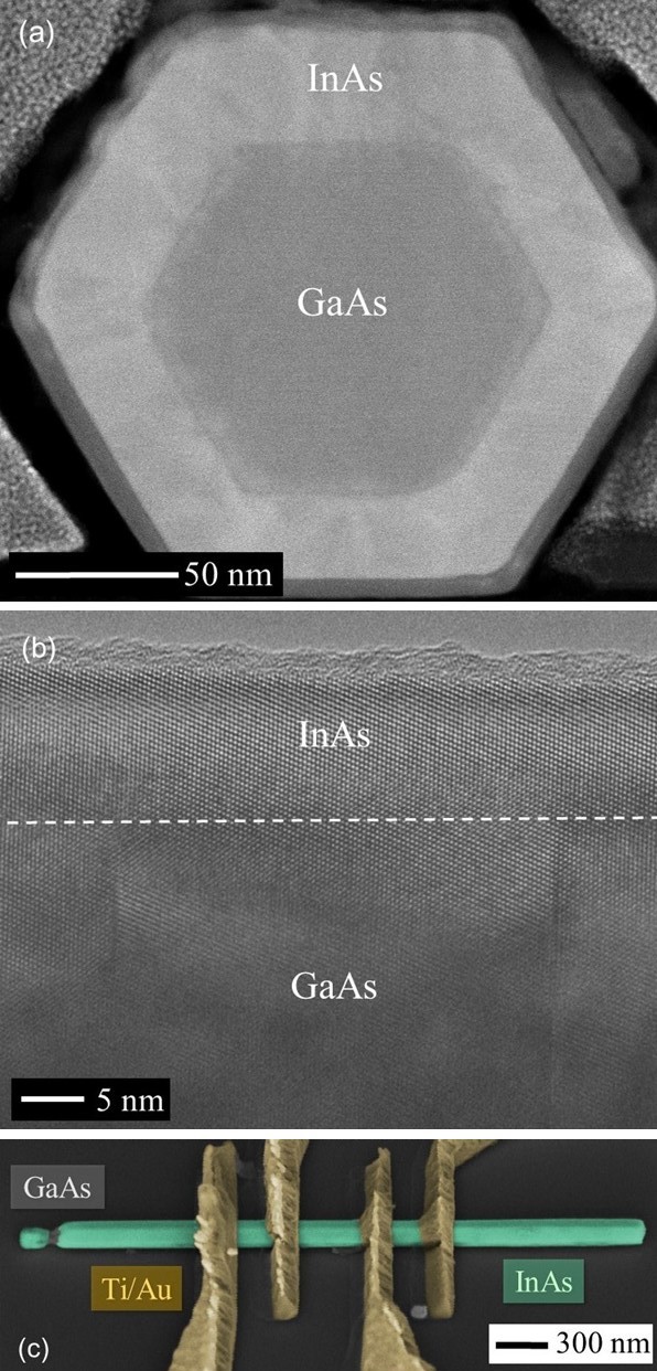
In this work, measurements are discussed on three samples, originating from two separate growth runs. In case of samples A and B the total growth time of 25 min for the InAs shell resulted in a smaller shell thickness compared to sample C with a shell growth time of 40 min (cf. Table 1). Figure 1 (a) corresponds to a low magnification annular dark field scanning transmission electron image (ADF-STEM) of the nanowire cross-section, i.e. along the 111 direction. Figure 1 (b) shows a high-resolution TEM image along the 110 direction. This type of images confirmed that ZB crystal structure is the preferred polytype both in the core and the shell. Detailed information on the growth procedure and the crystal structure is given in Supporting Information.
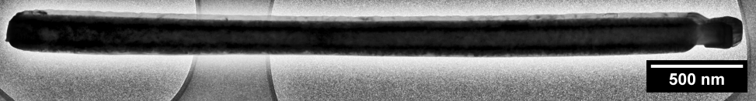
For the low-temperature transport experiments, the GaAs/InAs core/shell nanowires are transferred by a scanning electron microscope (SEM)-based micro-manipulator to a pre-patterned Si(100) substrate covered with of . Employing the precise nanowire transferring technique, as well as the electron beam lithography step and Ar+ cleaning, the metallization of Ti/Au contact fingers was realized. An example of a measured device is given in Fig. 1 (c). As previously mentioned, the measurement results of samples A and C are described here, with additional data from a second nanowire of the first growth run (sample B) summarized in the Supporting Information. The corresponding geometric dimensions of these nanowires are given in Table 1.
| Sample | (nm) | (nm) | (nm) | ||
|---|---|---|---|---|---|
| A | 51 | 28 | 79 | 400 | 3.3 |
| B | 58 | 27 | 85 | 400 | 2.7 |
| C | 56 | 39 | 95 | 450 | 4.6 |
The measurements were carried out in a variable temperature insert cryostat, with a base temperature of 1.5 K. Using a four-terminal measurement configuration and a standard lock-in setup, as well as applying an axial magnetic field, the devices were biased with a current of between the two outer contacts, whereas the voltage drop was measured between the two inner ones. The inner contact separation for the investigated samples is given in Table 1. The highly-doped Si substrate was used as a global backgate with the layer used as a gate dielectric.
III Results and Discussion
III.0.1 Gate dependence
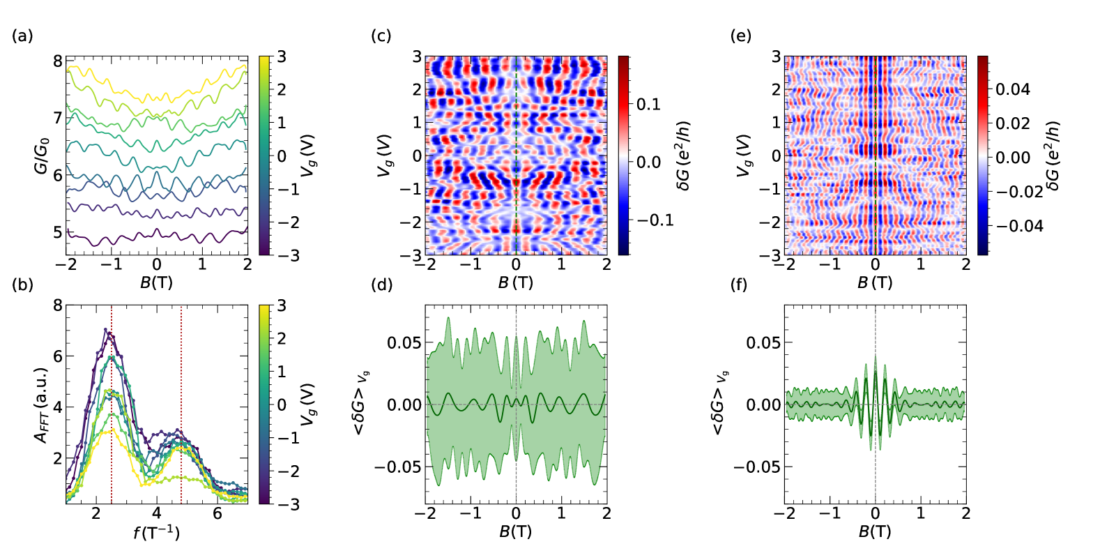
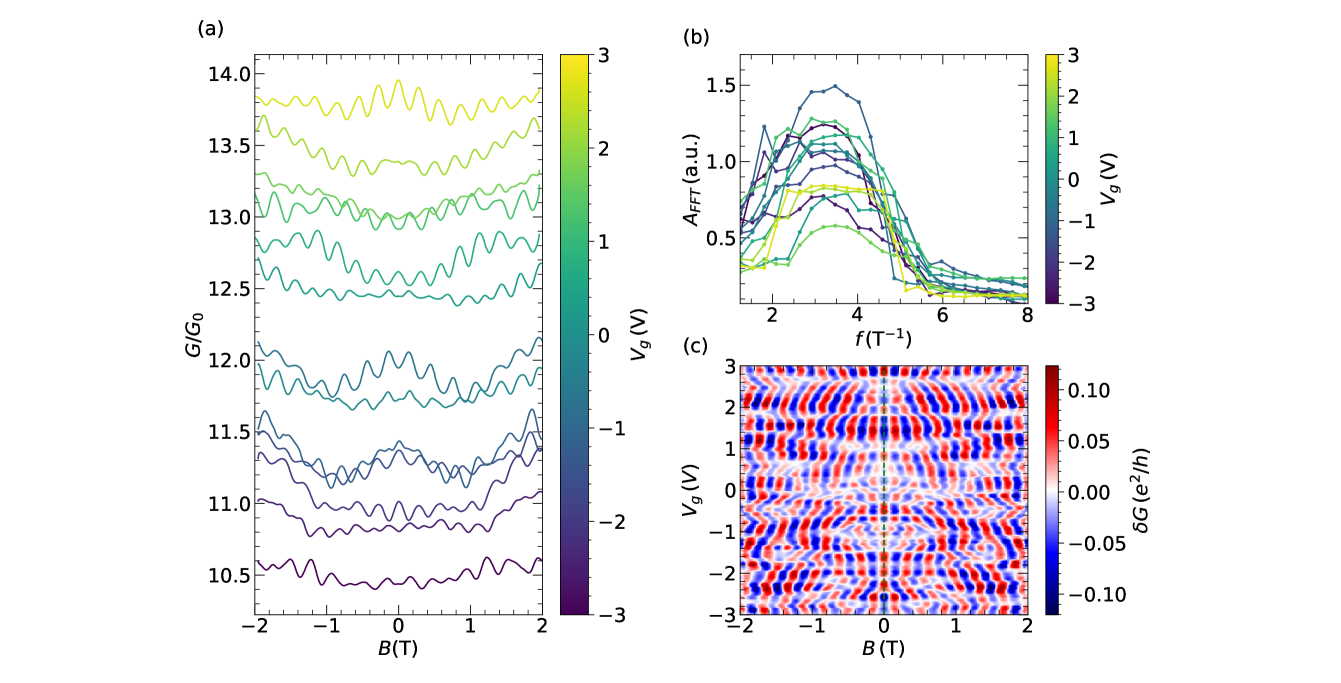
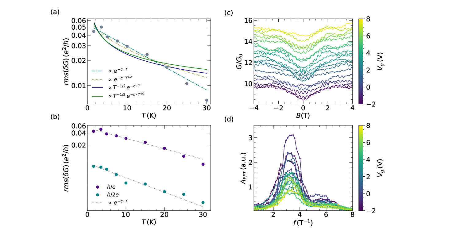
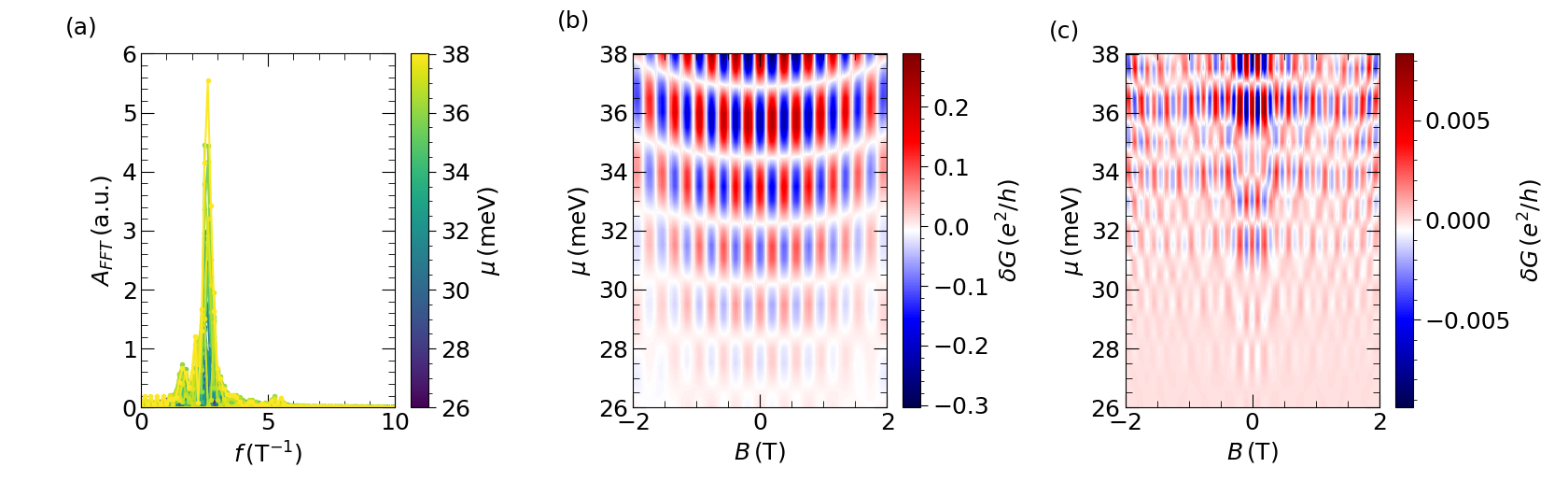
First, we focus on the gate-dependent magnetotransport properties of sample A (the corresponding measurements and analysis of samples B and C are given in Supporting Information). The measurements were conducted at 1.5 K in an axial magnetic field. A gate voltage ranging between and 3 V, with a stepping of V was applied to the global backgate. As shown in Fig. 2 (a), the normalized magnetoconductance , with , reveals regular AB-type oscillations over the entire gate voltage range.
From the oscillation period , the effective area enclosed by the closed-loop wave function can be determined by the relation , where is the magnetic flux quantum. Assuming a hexagonal nanowire cross-section, the area is given by , where is the the circumradius of the hexagon that is enclosed by the closed-loop wavefunction. For the extracted period of T, we get a radius of , confirming that the wave function is located within the InAs shell.
Aharonov–Bohm oscillations are related to a periodic modulation of the average occupation of the phase-coherent conducting states with different quantized transverse momenta enveloping the core [Guel2014]. By shifting the Fermi level position with the gate voltage, the average occupation is either forming a local maximum or minimum at , giving rise to phase jumps as a function of the gate voltage between and in the magnetoconductance oscillation pattern: , with the normalized magnetic flux and the gate voltage-dependent phase of the oscillation pattern. Note that the average occupation and the corresponding phase in the magnetoconductance oscillation pattern can vary over different parts of the sample under the change of local electron density in an environment of randomly distributed scattering centers within the InAs shell.
To further analyze the experimental data, a fast Fourier transform (FFT) of the magnetoconductance oscillations is performed. Before applying the FFT, the slowly varying background in the experimental data was subtracted from the measured conductance, resulting in an oscillation signal . As can be seen in Fig. 2 (b), the FFT spectrum obtained from measurements at different gate voltages systematically shows a two peak structure. The, first peak can be assigned to the AB oscillations with a period of while the second, smaller, peak corresponds a period of . The latter can originate from both AAS-type conductance oscillations or higher-harmonic contributions of the AB oscillations. The AAS oscillations result from interference of time–reversed paths in a tubular conductor [Altshuler1981, Sharvin81].
To gain a deeper insight into the physical origin of the two quantum transport contributions, we analyzed and compared the phase rigidity of the - and -periodic oscillations. For this purpose, the inverse Fourier transform of was evaluated. Furthermore, we isolated specific frequency windows in the Fourier spectrum corresponding to the peaks belonging to periods of and , respectively. Such an analysis is shown in Fig. 2 (c) for the -periodic oscillations, revealing a complex oscillation pattern with non-rigid phase as changes. Since the contribution dominates the oscillation pattern, the phase jumps along follow the phase jumps in the raw data. As a consequence of the random phase shifts with , the conductance averaged over the gate voltage basically cancels out while at the same time the standard deviation is very large, as can be seen in Fig. 2 (d). The oscillations, corresponding to the second peak in the FFT spectrum are not clearly visible in the raw data, i.e. in Fig. 2 (a), due to the dominance of -periodic oscillations. However, these oscillations are resolved in the inverse FFT spectrum shown in Fig. 2 (e). Interestingly, in a field range between and T, the -periodic oscillations are phase-rigid with a conductance maximum at zero field. Beyond this range the phase rigidity is weakened and eventually lost. The extent of the phase stability can also be deduced from Fig. 2 (f), which shows the conductance oscillations averaged over the entire gate voltage range . It can be seen that has its maximum value at and then decreases continuously with increasing field, disappearing completely at about T. The small standard deviation in this range underlines the claim of phase stability, as can be seen in Fig. 2 (f). We attribute the phase-rigid part to AAS oscillations. In terms of their rigidity while changing , AAS oscillations are robust to averaging since they originate from interference of time-reversed paths in our tubular InAs shell, as already resolved for polymorphic GaAs/InAs nanowires [Guel2014]. The conductance maximum at zero field indicates the presence of spin-orbit coupling due to the weak antilocalization effect [Aronov1987]. Such a conductance maximum has also been observed in bulk InAs nanowires [Estevez2010].
The phase-rigidity of the -periodic oscillation amplitude up to about T (cf. Fig. 2 (e)) can be explained by the finite thickness of the InAs shell and the corresponding loss of phase matching along the inner and outer radius when an axial magnetic field is applied. Using the approach outlined in Mur et al. [Mur2008], we obtained a limit of 0.17 T for our shell cross-section. This value is in relatively good agreement with the experimentally observed one. Beyond this magnetic field limit, the phase relation of the time-reversed paths is randomized [SLRen2015, CPUmbach]. At larger field strengths, the randomized phase relation suppresses the amplitude of oscillations, which can include higher-harmonic contributions of the AB oscillations as well. As a consequence phase rigidity is lost.
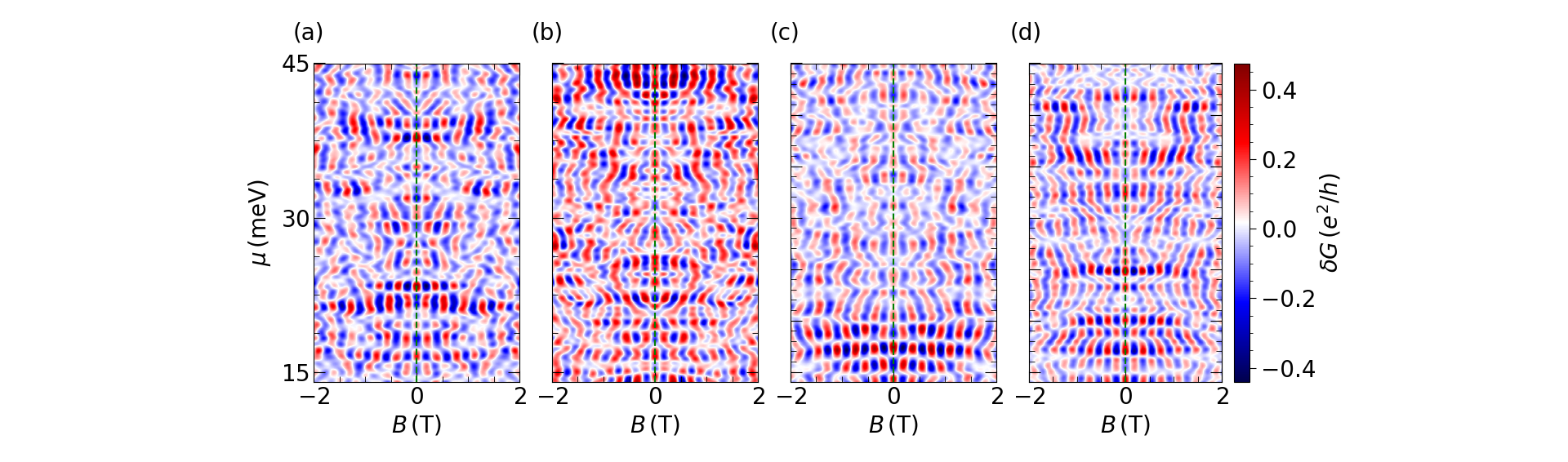
Several features of the experimentally observed oscillations can be reproduced by transport calculations based on linear response theory using the Kubo formalism [Kubo1957]. This is demonstrated in Fig. 3 (a), which shows the corresponding calculations of the magnetoconductance. The calculations were performed for the cross-sectional dimensions of sample A for different chemical potentials in the expected range of GaAs/InAs nanowires of similar dimensions [Guel2014, Haas2016], i.e. for our simulations we assumed a range between 26 and 38 meV. The Zeeman effect was included with a g-factor of [Winkler2003]. The general oscillation pattern as well as the phase jumps as a function of chemical potential are well reproduced. Furthermore, by changing the chemical potential, the phase of the oscillations switches. This is in agreement with the experimental results, since applying a gate voltage results in a shift of the chemical potential. However, Kubo formalism assumes an infinite wire length with included disorder. In this approach, the disorder is modeled as a system of uniformly distributed point scatterers, within the self-consistent Born approximation, as summarized in the Supporting Information. For the applied a disorder potential of 0.18 meV, we obtain oscillation amplitudes comparable to the experimental ones, although the total conductance is somewhat larger. Note, that higher order conductance corrections, represented by vertex or Cooperon diagrams, which are important to capture quantum interference effects, and in particular AAS oscillations, are not contained in our calculations. Thus, possible second harmonic features solely originate from the AB effect, due to discrete variation of the number of transverse channels when the magnetic field increases, the finite thickness of the tubular shell, or its non-circular (hexagonal) cross section.
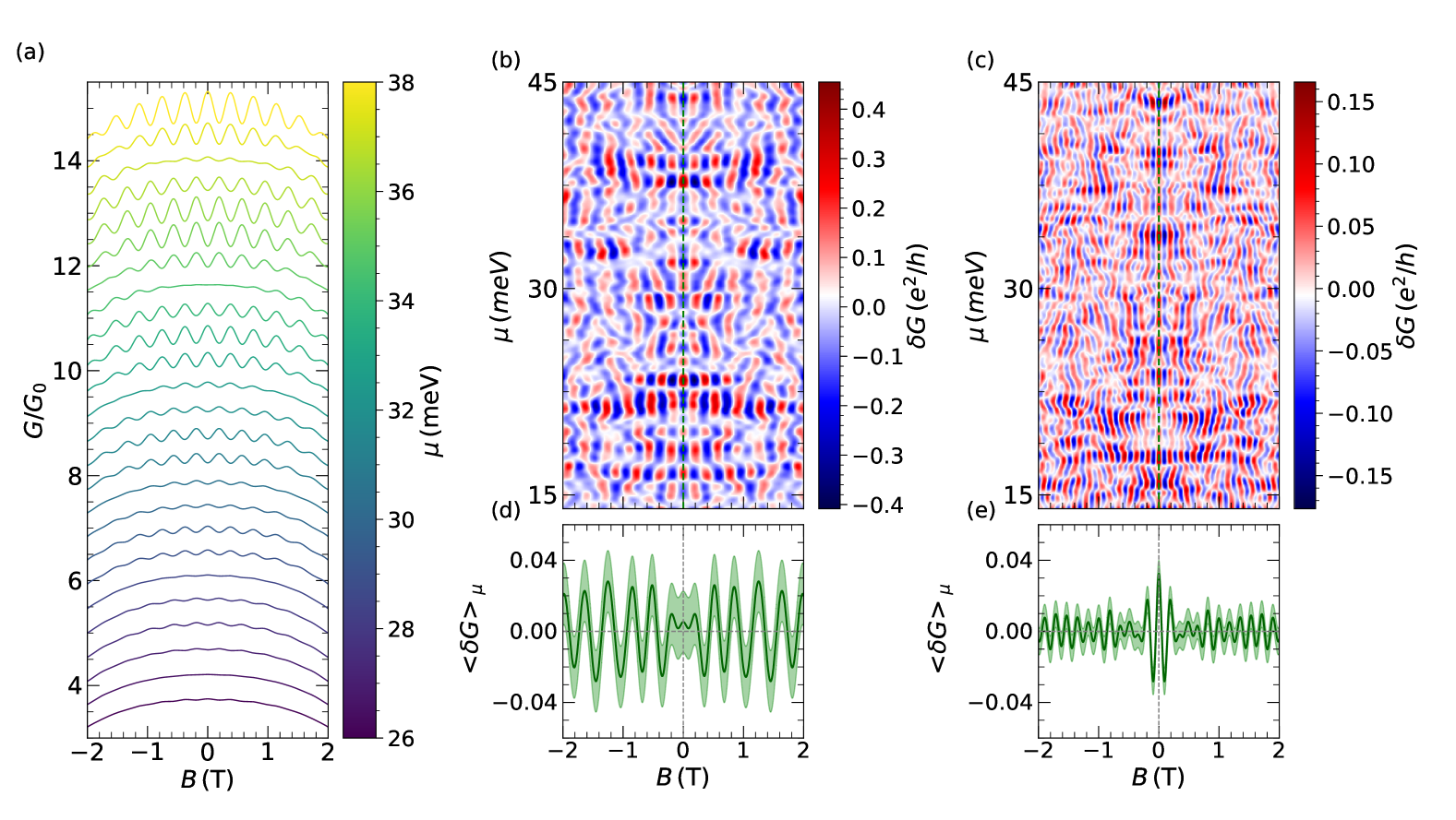
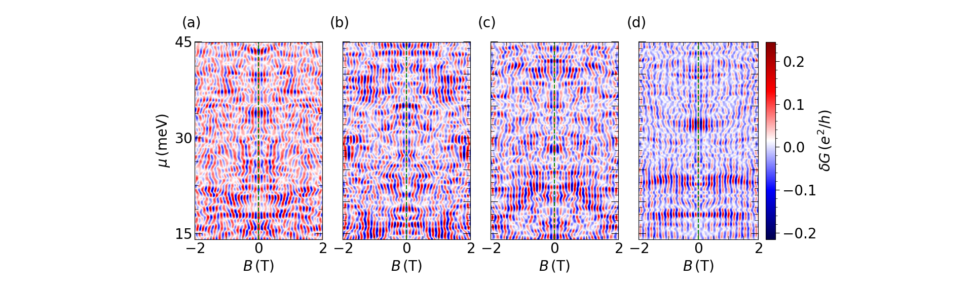
In order to include the AAS effect in the modelling, tight binding quantum transport simulations were performed using the software package KWANT [Groth2014]. In fact, by this, a regime can be explored, where the transport is governed by a finite number of scattering centers, being the appropriate scenario for our phase-pure nanowires. For the tight-binding description of the core/shell nanowire, a hexagonal cross-section corresponding to sample A and a wire length of 4 m was considered. For a direct comparison with the experimental values shown in Figs. 2 (c) and (d), the filtered first and second harmonics of the simulated conductance are plotted in Figs. 3 (b) and (c), as a function of magnetic field and chemical potential at a temperature of 1.5 K. The general features of the experimentally obtained results are reproduced by the simulations, i.e. the oscillations are non-phase-rigid, while for the oscillations, the phase rigidity is largely preserved around zero magnetic field. Furthermore, due to the implemented spin-orbit coupling in the simulations, a maximum of is found at zero field. To further support our reasoning, three additional simulations with different disorder configurations were performed. The results of each of these simulations are presented in the Supporting Information. Figures 3 (d) and (e) show the conductance oscillations averaged over the chemical potential as a function of magnetic field of the and periodic contribution, respectively. Each set is averaged over the chemical potential , and presented with the standard deviation. The average over the oscillations shows that the signal is significantly damped due to the phase changes with the chemical potential, and the standard deviation extends over a relatively large range. This indicates that the average phase for the four configurations differs to a large degree. In contrast, we find a different behavior for the averaged -periodic conductance contribution, as shown in Fig. 3 (e). A clear peak is observed at , consistent with phase-rigid AAS oscillations and the presence of spin-orbit coupling. Although a peak at is also observed for the oscillations, it does not correspond to robust phase rigidity. This can be seen from the large standard deviation of the pattern and the oscillation amplitude being much lower as compared to the typical oscillation patterns for fixed chemical potential. Interestingly, phase rigidity (associated with a maximum at zero field) was obtained only by considering the full length of 4 m of the nanowire, whereas by assuming a voltage probe separation of 400 nm, i.e. the separation of the inner contacts, only a random phase is found. We attribute this behavior to the fact that in the case of the 400 nm wire length, the number of scattering centers is too small to result in a sufficient number of time-reversed paths. It effectively means that the entire wire length is probed. Such a non-local transport effect is more commonly observed in mesoscopic conductors, which allow an extended region of the wire defined by to be probed regardless of the relatively small distances of the voltage probes [Umbach1987]. Summarizing these results, it appears that AAS oscillations show up in our measurements and simulations, which are usually attributed to higher-order scattering processes, despite the fact that the wire probably has a small number of scattering centers due to the phase purity of the crystal. To further clarify this issue and to find out about the relevant transport regime, temperature-dependent measurements were performed.
III.0.2 Temperature dependence
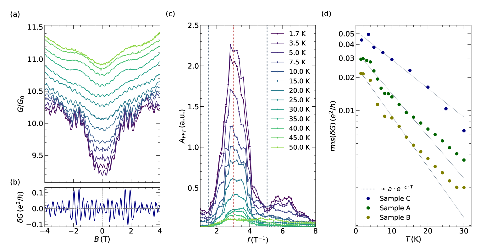
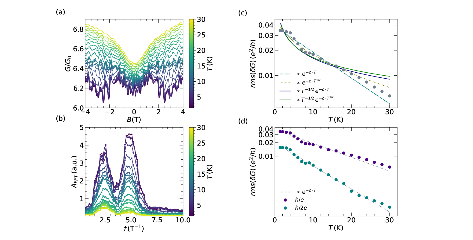
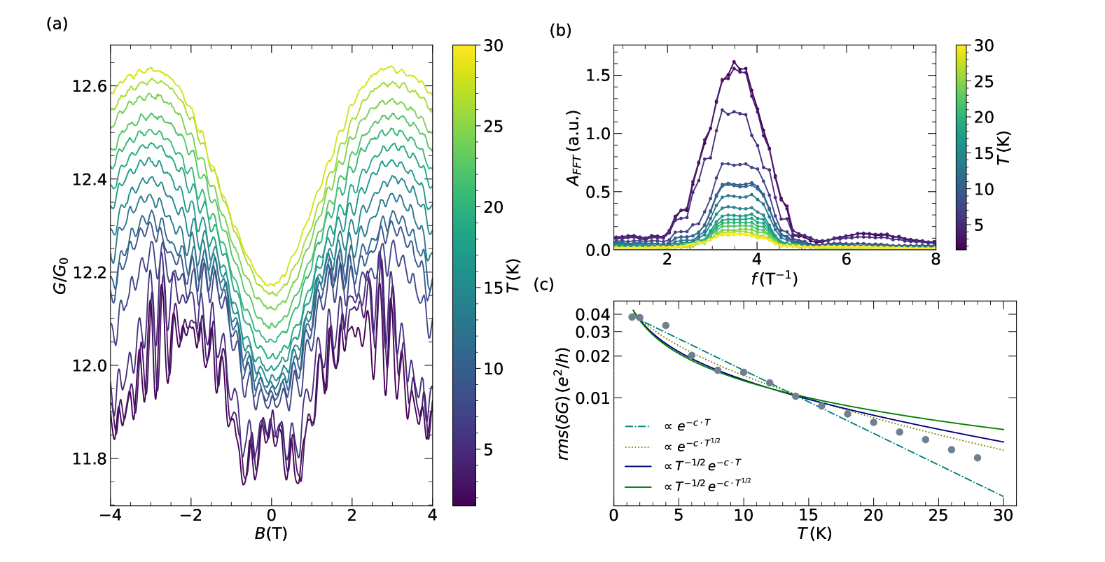
In this section, temperature-dependent magnetoconductance measurements for sample C are presented, whereas detailed corresponding descriptions for samples A and B are given in Supporting Information. Figure 4 (a) shows the normalized magnetoconductance as the temperature was varied from 1.7 to 50.0 K. Because of the different cross-section of sample C compared to A, here we find magnetoconductance oscillations, with a period of . The oscillations are superimposed on slower varying conductance modulations, corresponding to universal conductance fluctuations [Lee1987]. With increasing temperature, the number of inelastic scattering events increases, resulting in a reduction of the phase coherence length . This is manifested in a gradual decrease of the oscillation amplitude with rising temperature until they are completely suppressed at around 45.0 K. Figure 4 (b) shows the oscillation pattern at 1.7 K after subtracting the slowly varying background signal. The beating pattern found here is attributed to the effect of Zeeman splitting, which causes spin-dependent shifts in the flux parabolas of the energy spectrum [Rosdahl2014].
The periodic features in the magnetoconductance are analyzed in detail by applying an FFT, as presented in Fig. 4 (c). The FFT shows a clear peak at a frequency of about 3.0 T-1, corresponding to the extracted oscillation period given above. The frequency peak indicated by the red dashed line lies within the frequency limits given by the area defined by the inner and outer bounds of the InAs shell. Note that a peak belonging to the second harmonic frequency at about 6.0 T-1 is also observed. With increasing temperature, the peak amplitudes decreases, corresponding to a reduction in the oscillation amplitude. At about 45.0 K the peak is completely suppressed.
An essential insight into the phase-coherent transport of phase-pure core/shell GaAs/InAs nanowires under an in-plane magnetic field is provided by the temperature dependence of the -periodic oscillation amplitude [Haas2017]. To resolve it, the slowly varying background was first subtracted from the measured conductance, resulting in an oscillation signal , where the average oscillation amplitude is determined by the root mean square . Such analysis was carried out for all three samples, and Fig. 4 (d) shows the best fit for temperature dependence of . From this, it is possible to determine the phase coherence length , considering an exponential decay [Webb86]. For all samples, the resulting dependence can be fitted well to the data with . The exponential decay of the -periodic oscillation amplitude suggests a quasi-ballistic mesoscopic transport regime [Seelig2001]. Even though the experimental data at higher temperature seems to deviate from this fit, it still is the best representation for all three of our samples. Here, we compared between models that describe either the diffusive or quasi-ballistic transport regime, with or without thermal broadening. This is further displayed and discussed in the Supporting Information. The obtained dependence is in contrast to previous measurements on core/shell GaAs/InAs nanowires, where a dependence with of about 0.6 was extracted [Haas2017], which is close to the diffusive case [Ludwig2004]. We attribute the different behavior to the improved crystal quality of the present nanowires. From the fit, we determined at base temperature for each sample (cf. Table 1). As expected for the ballistic case, exceeds the length of the ring-like tubular conductor arm and is found to be significantly larger than previously reported for GaAs/InAs nanowires [Haas2017]. Additionally, it is in good agreement with the proposed superior transport properties of phase-pure core/shell nanowires. A quasi-ballistic transport regime has also been observed in topological nanowire structures, where spin-momentum locking is assumed to be responsible for the reduced scattering [Dufouleur2013, Ziegler2018, Rosenbach2022].
IV Conclusions
In conclusion, phase-coherent transport is studied in phase-pure zincblende GaAs/InAs core/shell nanowires. Pronounced Aharonov–Bohm oscillations with a period of are observed. These oscillations arise from the presence of coherent closed-loop states in the InAs shell, which are periodically modulated when a magnetic flux is threaded through the wire cross-section. In contrast to previous studies, the temperature dependence of the oscillation amplitude indicates that the transport takes place in the quasi-ballistic regime. When the electron concentration is varied by a back-gate voltage, the phase of the -periodic oscillations are found to be non-phase-rigid, which is attributed to the lack of time-reversal symmetry of this interference process. Interestingly, the oscillation component contains a phase-rigid region around zero magnetic fields. This can be explained in the framework of Althshuler–Aronov–Spivak oscillations, where time-reversal symmetry is preserved. It is noteworthy that these oscillations are observed in the quasi-ballistic regime and not, as usual, in the diffusive regime. At larger magnetic fields, only the second harmonic of the Aharonov–Bohm oscillations remains. The findings on the presence or absence of phase rigidity of the -periodic oscillations are confirmed by quantum transport simulations, where a relatively small number of scattering centers, represented by a disorder potential with a correlation length of 50 nm, are found to conform to the quasi-ballistic regime and still give rise to phase-rigid Altshuler–Aronov–Spivak oscillations near zero field. The phenomena and the transport regime observed here are very similar to experiments on topological insulator nanoribbons, despite the absence of spin-momentum locking in our case. The quasi-ballistic transport behavior in our nanowires confirms the expected superior quality of the phase pure crystal structure, which is highly relevant for the reproducible definition of confined quantum states. The results obtained here are also important for future superconductor/semiconductor nanowire hybrid structures, e.g. for topological [Oreg2010, Lutchyn2010, Prada2020] or Andreev-level qubits [Zazunov2003, Tosi2019, Metzger2021, Zellekens2022]. An important aspect in this context is the coupling of the superconducting shell with the electron gas at the interface, which is favorably achieved by confining the electron system in the shell. In fact, when coupled to a superconducting contact, enhanced magnetoconductance oscillations with a period of are observed, which are attributed to phase-coherent resonant Andreev reflections [Guel2014a]. More recently, oscillations have been found in the switching current of Josephson junctions based on GaAs/InAs core/shell nanowires [Zellekens2024]. In light of these recent experiments, we believe that phase-pure semiconductor nanowires present a very interesting new research direction towards optimization of such hybrid devices.
Acknowledgements
We thank Herbert Kertz for technical assistance. Dr. Florian Lentz and Dr. Stefan Trellenkamp are gratefully acknowledged for their help with the required e-beam lithography. The sample fabrication has been performed in the Helmholtz Nano Facility at Forschungszentrum Jülich [Albrecht2017]. This work was partly funded by Deutsche Forschungsgemeinschaft (DFG, German Research Foundation) under Germany’s Excellence Strategy—Cluster of Excellence Matter and Light for Quantum Computing (ML4Q) EXC 2004/1—390534769. K.M. acknowledges the financial support by the Bavarian Ministry of Economic Affairs, Regional Development and Energy within Bavaria’s High-Tech Agenda Project ”Bausteine für das Quantencomputing auf Basis topologischer Materialien mit experimentellen und theoretischen Ansätzen” (Grant No. 07 02/686 58/1/21 1/22 2/23) and by the German Federal Ministry of Education and Research (BMBF) via the Quantum Future project ‘MajoranaChips’ (Grant No. 13N15264) within the funding program Photonic Research Germany. A.M.S. and R.J. acknowledge the support of the EPSRC Grant EP/W002418/1.
References
Supporting Information: Aharonov–Bohm and Altshuler–Aronov–Spivak oscillations in the quasi-ballistic regime in phase-pure GaAs/InAs core/shell nanowires
SUPPLEMENTAL NOTE 1: Experimental Details
The MBE growth of hexagonal-, or cubic-phase-pure GaAs core nanowires via self-catalysed vapour-liquid-solid technique on pre-structured substrates requires precise and dynamic control over the catalyst droplet on top of the growing nanowires. The evolution of the droplets contact angle over time determines the boundaries of axial phase changes along the nanowires. Following the recently developed approach of Jansen et al. [Jansen2020], a contact angle of the Ga catalyst droplet around is appropriate to favour the wurtzite (WZ) phase or alternatively, above , to aim for the zincblende (ZB) phase of the GaAs core. In Ref. [Jansen2020] we achieved the stabilization of the contact angle around by a dynamical reduction of the Ga flux by about % during a growth time of 90 min. However, this WZ phase stabilization regime is extremely sensitive to the properties and precision of pre-structuring the substrates. For the as-grown nanowires we used Si(111) substrates covered with about 20 nm of thermally deposited Si hole arrays with varying diameters of 40, 60, and 80 nm and pitches with 0.5, 1, 2, and 4 m pinhole distances. These were predefined by electron beam lithography and subsequent dry and wet etching of the down to a remaining thickness below 1 nm. Note that precision of hole aspect ratio and etching depth is mainly limited by the etching processes used and can induce statistical deviations from the above-mentioned ideal stabilization conditions of the Ga catalyst droplet. After preparation, the pre-structured substrates are loaded into the load-lock of our MBE system and baked-out for about 45 min at C. Then, the samples are transferred to the III/V-MBE chamber, heated to a substrate temperature of about C and Ga is deposited for 10 min at a Ga beam equivalent pressure (BEP) of about mbar. During this step the Ga-droplets in the holes are formed, which under optimum conditions of the above-mentioned pre-structuring yield a starting contact angle around . Following the pre-deposition of Ga, the growth of the GaAs core is initiated by applying an As flux with a BEP of mbar for 90 min at the same substrate temperature, while the Ga flux is dynamically decreased to 60 % of the starting value. With the present growth conditions, a contact angle above is achieved, resulting in a zincblende crystal phase. The GaAs core growth is finalized with a 20 min long droplet consumption step under reduced As BEP of while the substrate temperature is kept at about C. The InAs shell growth of the first growth run (samples A and B) is performed in total for 25 min divided into 5 cycles, each one with 5 min of growth alternated by 5 min of growth break under As-stabilization. The corresponding substrate temperature is C. In and As were supplied with BEPs of mbar and mbar, respectively. In case of the second growth run (sample C) the shell was grown for 40 min with according growth breaks, i.e. 8 cycles instead of 5.
SUPPLEMENTAL NOTE 2: Transmission Electron Microscopy Studies
In order to analyze the crystal structures at different locations along the nanowire by transmission electron microscopy (TEM), they are transferred onto a lacey carbon grid. The nanowires were examined by a JEOL 2100 TEM operated at 200 keV. Supplemental Figure S1 shows a bright-field transmission electron micrograph (BF TEM) of a typical nanowire of the first growth run (representative samples A and B) with a length of 3.8 m and diameter of 210 nm in the middle part.
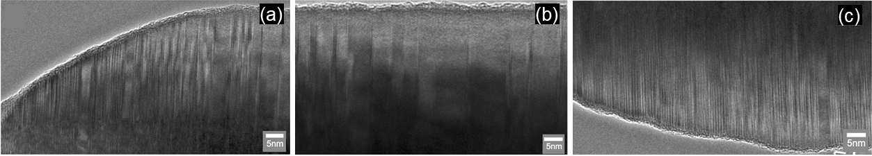
Supplemental Fig. S2 (a) shows a high-resolution TEM (HR TEM) image of the top part of the nanowire, confirming the presence of stacking faults and different crystal phases. Supplemental Fig. S2 (b) depicts the HR TEM image of the middle part of the nanowire showing only zincblende segments with twins. Finally, in Supplemental Fig. S2 (c), the bottom part is shown revealing once again stacking faults and different crystal phases.
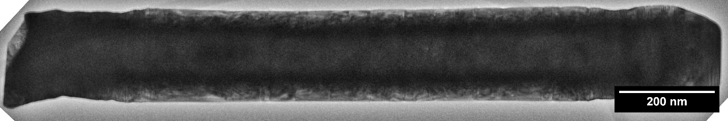
Supplemental Fig. S3 shows a BF TEM micrograph of a typical nanowire of the second growth run (representative sample C) with a length of 1.5 m, and average diameter of 188 nm.
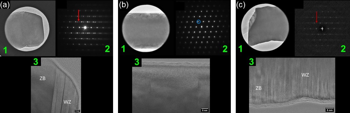
Supplemental Fig. S4 (a) shows the selected-area image (1) of the nanowire top part and (2) is the corresponding selective-area electron diffraction (SAED) pattern. The streaky pattern (indicated by a red arrow in (2)), suggests the presence of stacking faults and different crystal phases. Subfigure (3) is the HR TEM image of the top part of the nanowire confirming the presence of WZ and ZB segments. A number of WZ segments were observed with a length of 18 and 11 nm.
In Supplemental Fig. S4 (b) (1), the selected-area image of the middle part of the nanowire is shown with the corresponding SAED pattern given in (2). The streaky pattern is not observed in the SAED pattern. A pair of spots are observed (indicated by blue circle), suggesting the presence of twins and the absence of streaks indicate longer ZB segments. In Subfigure (3), showing the corresponding HR TEM image, ZB segments with twins can be identified.
Supplemental Fig. S4 (c) (1) is the selected-area image of the nanowire bottom, and (2) is the corresponding diffraction pattern. The streaky pattern (indicated by a red arrow) indicates the presence of stacking faults and different crystal phases. In the HR TEM image given Subfigure (3), stacking faults along with ZB and WZ segments are revealed, i.e. supporting the observed diffraction pattern. A WZ segment was found at the bottom of the nanowire with a length of 5 nm.
SUPPLEMENTAL NOTE 3: Additional Magnetotransport Measurements
A Sample A
The temperature-dependent normalized magnetoconductance measurements on sample A are presented in Supplemental Fig. S5 (a), with . The conductance was measured as a function of axial magnetic field in the range of to 4 T for temperatures between 1.4 and 30 K. Regular oscillations in the conductance signal with an Aharonov–Bohm (AB) period of 0.4 T are observed. From this measurement it can be concluded that periodic oscillations persist up to about 30 K. This agrees well with the fast Fourier transform (FFT) data analysis of the measurement (see Supplemental Fig. S5 (b)), where a peak is observed at a frequency of , and a second peak corresponding to periodic oscillations is found at 4.8, which fits well with the observed values in the gate-dependent measurements presented in the main text.
The temperature-dependent magnetoconductance measurement on sample A allows a detailed analysis of the transport regime by estimating the temperature dependence of the AB oscillation amplitude [Webb86, Seelig2001]. Supplemental Fig. S5 (c), shows different fits corresponding to cases of transport, i.e. given with a prefactor to account for when the thermal energy is larger than the Thouless energy, or without thermal broadening, as well as diffusive , and quasi-ballistic transport regime. It can be concluded that the quasi-ballistic fit without thermal broadening follows our data best.
Additionally, Supplemental Fig. S5 (d) demonstrates the quasi-ballistic fit for both - and -periodic oscillations by extracting the , using the inverse FFT method with pre-defined frequency windows for -, and -periodic oscillation peaks. From the data presented, it can be concluded that such a fit can well describe both, , and conductance contributions in our data. In case of conductance contribution temperature dependency, a fit parameter of value , was extracted, and the phase-coherence length was estimated to be 3.3 m.
B Sample B
As for sample A, the analysis of the temperature-dependent magnetoconductance measurement results of sample B is discussed in the following text. The normalized conductance is shown as a function of axially applied magnetic field in the Supplemental Fig. S6 (a). Pronounced AB-type oscillations with a periodicity of 0.3 T are observed, which persist up to about 30 K. A beating pattern is observed in the magnetoconductance up to a temperature of about 12 K. We attribute this to the presence of Zeeman splitting [Rosdahl2014]. The oscillation period agrees well with the position of the frequency peak at 3.5 in the FFT analysis, shown in Supplemental Fig. S6 (b). This value corresponds to the mean radius of the coherent trajectory of 67 nm. A relatively small second peak is observed at about 6.6, which vanishes around K. Conducting the same transport regime analysis, by evaluating the AB oscillation amplitude temperature dependency, as shown in Supplemental Fig. S6 (c), we could conclude that the quasi-ballistic fit describes our data very well. From this, fitting parameter was extracted, and the phase-coherence was estimated as .
In Supplemental Fig. S7 (a) the magnetoconductance is shown for different values of the applied gate voltage ranging from to 3 V. The axial magnetic field was applied from to 2 T. Regular oscillations are seen with varying conductance minima and maxima at . The corresponding FFT analysis of this data is shown in Supplemental Fig. S7 (b). In this measurement, no signs of conductance contributation is found. The gate-dependent measurement shown here was performed after the temperature-dependent one, so it can be argued that due to multiple thermal cycles, the potential landscape in the nanowire has changed significantly, leading to absence of such contribution. To further illustrate the evolution of the periodic oscillations across the gate voltage range, the filtered out conductance contribution is given by the colormap in Supplemental Fig. S7 (c). Phase jumps between 0 and are clearly observed at .
C Sample C
In the main text, a detailed analysis of temperature-dependent magnetoconductance measurements for sample C is given. As an additional support to the transport regime evaluation, Supplemental Fig. S8 (a) features four different transport regime fits, as described in the previous sections. This graph demonstrates the quasi-ballistic fit as a good way to describe the transport regime in our sample. From the quasi-ballistic fit, using the extracted fitting parameter , the phase coherence length was determined to be . In addition, Supplemental Fig. S8 (b) shows that such a fit describes both and conductance contributions well.
Furthermore, Supplemental Fig. S8 (c) shows the gate-dependent magnetoconductance for applied gate voltage in the range from to V in steps of 0.25 V at a temperature of 1.5 K. Once again, persistent AB oscillations are observed for the entire gate voltage range. Similar to the case of temperature-dependent measurement, a -periodic contribution peak in FFT analysis (Supplemental Fig. S8 (d)) is observed at , whereas the second peak, corresponding to the contribution, is found at , and vanishes around V.
SUPPLEMENTAL NOTE 4: Modelling using Kubo Formalism
Using the Kubo formalism, the magnetoconductance was calculated for a nanowire with geometrical dimensions similar to those of sample A. The nanowire was described as a tubular shell with infinite length, and with an external radius . The InAs material was represented by the effective mass and by the factor of . The transverse section was discretized on a polar lattice [Sitek2015, Manolescu2017]. The eigenstates of the Hamiltonian were obtained by numerical diagonalization and were labeled as , where is the wave vector of the plane waves in the longitudinal direction , labels the transverse modes, and is the spin index. For this nanowire model the conductivity was calculated with the linear-response Kubo formula,
| (S1) |
where is the transverse area of the shell conductor, the velocity operator in the -direction, the Fermi function, and the Green’s function [Urbaneja2018]. The nanowire includes disorder implemented as uniformly distributed point-like impurities, which generate the energy dependent self-energy . In the present simple approximation is considered a complex number, which is obtained by an averaging procedure over all possible impurity configurations, in the self-consistent Born approximation [Doniach1998]. That procedure leads to solving the equation
| (S2) |
with being an energy parameter associated with the impurities.
To compare with the experimental data we converted the conductivity to conductance, by multiplying Eq. (S1) with the factor , where is the length of the nanowire. In the main text the normalized magnetoconductance is presented as a function of the chemical potential (see e.g. Fig. 3 (a) in the main text), for disorder potential meV and temperature K. The change in chemical potential is directly related to the change in gate voltage in the experiment. With increasing gate voltage and thus increasing carrier concentration, the chemical potential increases accordingly. The obtained Kubo formalism calculations capture the basic features of the measurements, where the magnetoconductance increases with increasing chemical potential and oscillates with the period of a magnetic flux quantum . The phase of the oscillations changes with the chemical potential, which was also observed in the experiment, see e.g. Fig. 2 (c) in the main text.
Additional to the normalized magnetoconductance plot shown in main text, Supplemental Fig. S9 (a) displays the FFT analysis of the presented data with subtracted background () for a chemical potential ranging from 26 to 38 meV. These calculations feature similar and peak positions on the frequency scale, as compared to the experimental values of sample A.
By individually analysing these frequency windows, a chemical potential-dependent phase analysis could be made, following the same method as for our experimental data. In Supplemental Fig. S9 (b), the contribution is presented, showing the expected phase switching over the entire chemical potential range along the line. However, the same analysis of the isolated contribution presented in Supplemental Fig. S9 (c), does not reveal any phase-rigidity at the line. In fact, in the calculations using the Kubo formalism, higher order terms are not included, so we do not expect any phase rigid contributions arising from localization effects. We therefore attribute the observed second harmonic in the FFT to non-sinusoidal contributions of the Aharonov–Bohm type oscillations.
SUPPLEMENTAL NOTE 5: Tight Binding Simulations using KWANT
A tight binding model representing the GaAs/InAs core/shell nanowire system is created with the package Kwant [Groth2014]. This model is an adaptation of the model presented in Ref. [Bommer2019], starting from the following continuum model Hamiltonian:
| (S3) | |||||
The Hamiltonian consists of three terms: the first term describes the quadratic dispersion of a free electron gas with wave vector and effective mass , also including the chemical potential and potential that describes all remaining potentials present within the model. Inside the core, this potential is taken to be 1 eV (neglecting disorder) while in the shell the potential represents the disorder, described by a Gaussian random field with disorder strength and correlation length . This correlation length is chosen rather comparable to the length of the wire (significantly exceeding the atomic scale), in order to represent a phase-pure nanowire in the quasi-ballistic regime with few scattering centers over the length of the transport section. An example of such a disorder profile is given in Supplemental Fig. S10.

The second term of the Hamiltonian covers the spin-orbit coupling with respect to a specific surface, for which the surface normal is orthogonal to the -axis. We take , with , as the Pauli matrices acting on the spin (and the identity matrix). In the spin-orbit term, is the spin-orbit coupling strength, while the angle depends on the location of the site in question. The angle is defined so that the spin-orbit coupling is given in the direction of the nearest surface facet, which is expected to be the dominant orientation of spin-orbit coupling in the nanowire under consideration.
The third term of Eq. (S3) is the Zeeman term, with the g-factor and the Bohr magneton. The magnetic field under consideration is applied along the -direction and given by , with corresponding vector potential . This vector potential was implemented using the Peierls substitution method.
The continuum model Hamiltonian is discretized using the finite difference method on a cubic lattice with a lattice constant that is sufficiently small to fit at least two layers of sites in the shell to represent the conducting modes enveloping the core. This discretization scheme is sufficient to capture the appearance of AB and AAS oscillations but is probably not sufficient to capture the loss of phase matching due to the finite thickness of the shell, as seen in experiment.
The model consists of a scattering region with two semi-infinite leads attached at opposite ends. The only difference between the Hamiltonian in the leads and the Hamiltonian in the scattering region is the added disorder in the scattering region as a function of . The nanowire itself has a hexagonal shape for the core and shell, the approximate outer radii of which are 55 nm and 85 nm, respectively, comparable to the dimensions of sample A. The hexagonal shape can be seen in Supplemental Fig. S10. The relevant simulation parameters are summarized in Supplemental Table 1.
| Parameter | Value |
|---|---|
| nm | |
| nm | |
| nm | |
| 10 nm | |
| 14 - 45 meV | |
| 20 meVnm | |
| 1 eV | |
| 5 meV | |
| 1.7 K |
The magnetoconductance was obtained as a function of the magnetic field and chemical potential through the Landauer formula and scattering matrix calculations in Kwant:
| (S4) |
with Fermi function and transmission probability over the scattering region (summed over all channels). Note that energy and chemical potential can be interchanged, , and furthermore , such that the finite-temperature conductance can be evaluated from transmission probabilities at zero energy, obtained over a range of chemical potentials and positive magnetic field strengths.
Supplemental Figs. S11 (a) to (d) show the filtered -periodic conductance contributions as a function of magnetic field and chemical potential . In total, four different sets of disorder potential configurations in InAs shell are considered, each with a disorder strength of 5 meV, with the conductance evaluated at a temperature of 1.7 K. The first of this set is presented and discussed in the main text, whereas the remaining three are briefly summed up in this section.
For all disorder configurations we find that the phase at zero magnetic field switches between 0 and . However, the chemical potential values at which this switching occurs are different for each configuration. The phase is balanced between 0 and with a small tendency towards a conductance peak, i.e. phase 0. Furthermore, the phase also switches randomly at finite magnetic fields.
Supplemental Figs. S12 (a) to (d) show, similarly to Supplemental Figs. S11, the corresponding filtered -periodic conductance contributions. For all generated sets of disorder potential configurations, we predominantly find a peak at , with only very short sections where the phase is switched.
This finding is in agreement with our experimental observation of phase rigidity around zero magnetic field due to the occurrence of Altshuler–Aronov–Spivak oscillations in the presence of spin-orbit coupling. In the main text, the results for the different disorder configurations presented in Supplemental Figs. S12 and S11 are further discussed with respect to their average properties.
Finally, we also present the magnetoconductance results that are obtained for a nanowire segment that is only 400 nm long, with all other simulation parameters kept fixed.
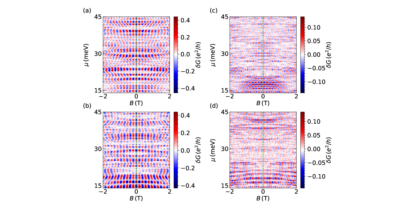
This distance corresponds to the inner contact separation, between which the voltage drop was recorded. In Supplemental Figs. S13 (a) and (b), examples of the isolated conductance contributions are presented for the case of two different sets of calculations comprising different potential landscape profiles. As expected, for both sets we observe phase switching along the line, associated with AB oscillations. However, for the corresponding filtered out conductance contribution shown in Supplemental Figs. S13 (c) and (d), no prominent peak along the line is found. As discussed in the main text and in Supplementary Note 4, such a feature is more likely to represent a second harmonic contribution of the AB oscillations than of the AAS oscillations.