Gate-tunable band-edge in few-layer MoS2
Abstract
Transition metal dichalcogenides (TMDs) have garnered significant research interest due to the variation in band-edge locations within the hexagonal Brillouin zone between single-layer and bulk configurations. In monolayers, the conduction band minima are centered at the -points, whereas in multilayers, they shift to the -points, midway between the and points. In this study, we conduct magnetotransport experiments to measure the occupation in the and valleys in four-layer molybdenum disulfide (MoS2). We demonstrate electrostatic tunability of the conduction band edge by combining our experimental results with a hybrid tight-binding model that accounts for interlayer screening effects in a self-consistent manner. Furthermore, we extend our model to bilayer and trilayer MoS2, reconciling prior experimental results and quantifying the tunable range of band edges in atomically thin TMDs.
I Introduction
Transition metal dichalcogenides (TMDs) display unique electronic [1, 2, 3] and optical properties [4, 5]. A key feature of TMDs is the presence of multiple valleys in their band structure, with the conduction band hosting valleys at both the points and the points (located midway between the and points) of the first Brillouin zone, while the valence band exhibits valleys at the points and the point [6]. The relative energy levels of these valleys are strongly influenced by the number of layers, leading to layer-dependent modifications in the band structure [7, 8].
In our previous studies, we systematically investigated the conduction band of single layer [9], bilayer [10], and trilayer MoS2 [11]. We found that electron transport predominantly occurred via the valleys of the conduction band, while the occupation of valleys, predicted by theory [12, 13, 14, 15, 16, 17], was not detected in our measurements. In these studies, we employed electrostatic gating to overcome the Schottky barrier that typically forms at the metal-MoS2 interface. However, the influence of the gate-induced electric field on the band structure, particularly the relative energy shift of different valleys [18], was not considered.
Here, we investigate four-layer MoS2, where we observe a gate-dependent band edge transition in the conduction band minima, shifting from the valleys at low gate voltages to the valleys at higher voltages. This transition reveals the sensitivity of the conduction band to external electric fields, which we attribute to the differing atomic orbital compositions of the and valleys, as well as interlayer screening effects. Our findings not only demonstrate the coexistence of both and valleys in biased four-layer MoS2, but also show how electrostatic gating can effectively tune the band structure in TMD-based devices. These results offer deeper insights into the electronic properties of multilayer MoS2 and present potential avenues for valley-selective device applications.
II Results and discussion
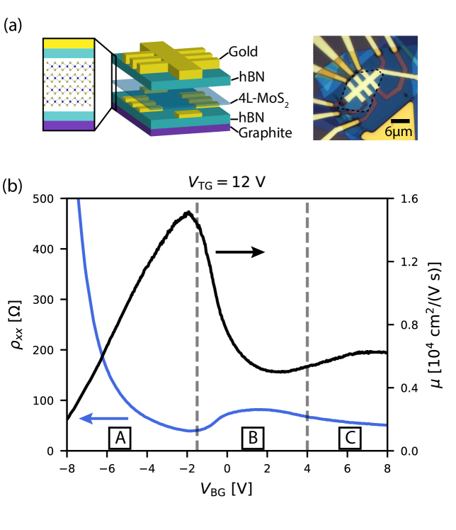
In this study, we use dual-gated, multi-terminal devices, as shown in Fig. 1(a). The devices are heterostructures consisting of four-layer MoS2 encapsulated in hexagonal boron nitride (hBN), all obtained by mechanical exfoliation. We conducted the experiments on two samples: Sample A, featuring a graphite bottom gate and a metallic top gate, and Sample B, with metallic gates on both sides. The results presented in the main text are from Sample A, which exhibits higher electron mobility and more pronounced Shubnikov-–de Haas oscillations (SdHO). Similar results obtained in Sample B are provided in the Supplementary Information.
One of the challenges of electronic transport experiments in MoS2 devices is achieving ohmic contacts. This issue is effectively addressed by employing a sample geometry with gated metallic contacts [2, 19, 20, 9, 21]. In such samples, finite conductance at cryogenic temperatures is achieved only at relatively large top gate voltages (), which are required to overcome the Schottky barrier at the metal-MoS2 interface.
For this reason, in our experiments, we fix the top gate voltage and tune the density with the bottom gate voltage (), which does not affect the electron density in the region of the contacts due to the screening provided by the metallic contact pads. This enables us to maintain low-resistive () ohmic contacts for all densities in the Hall bar. However, this sample geometry restricts the parameter space spanned by the gates. As a consequence, the samples are typically operated under finite electric displacement field (), which affects the electron distribution across layers in multilayer MoS2, potentially affecting their electronic properties.
In Fig. 1(b), we present the resistivity (blue) as a function of measured at and a temperature of . The resistivity reveals a non-monotonic dependence on , which is also evident in the transport mobility (black). The mobility increases roughly linearly in the voltage range (regime A in the figure), reaching a peak value of at an electron density of approximately . Further increasing results in a significant drop in mobility, which we attribute to the population of a second band, similar to our observation in three layer MoS2 samples [11].
To investigate the contribution of the different bands in four-layer MoS2, we examine the data obtained at finite magnetic fields. In Fig. 2(a), we present the magnetoresistance as a function of measured at . This measurement reveals an intricate pattern that originates from overlapping Landau fans. The observation of multiple Landau fans confirm the existence of multiple electronic bands.
Each of those bands has a corresponding electron density which determines the frequency of the SdHO. We extract the densities by computing the Fast Fourier Transform (FFT) of (see details in the Supplementary Information) and plot the resulting densities in Fig. 2(b). In the voltage range (regime A), the Fourier analysis reveals two electron densities, and (blue and green curves), both with a similar gate voltage dependence. The densities are calculated using the relationship , where is the frequency, is the degeneracy of band , is the elementary charge and is Plank’s constant. By comparing the sum (gray curve) to the total density obtained from the Hall effect measurements (red curve), we determine a degeneracy of for both bands. This degeneracy suggests that the bands are centered at the points of the Brillouin zone.
The density difference arises from the spin-orbit splitting of the valley. By linear extrapolation, we estimate at the onset of the density , which aligns with the density required to populate the upper spin-orbit split band at the points observed in previous studies in monolayer [9], bilayer [10], and three-layer [11] MoS2. This further supports our interpretation.
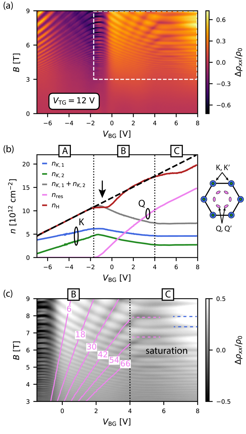
Now, we turn our attention to regime B in Fig.2(b), where an additional band starts getting populated. This is evident in three distinct aspects. The first is the emergence of another Landau fan in Fig.2(a) (highlighted by the white dashed frame), with its origin around . At the same gate voltage, the Hall density exhibits a plateau (marked by an arrow), which we attribute to the filling of defect states at the bottom of the newly occupied band. This results in the localization of electrons at the defects, preventing them from contributing to the Hall effect (see also the Supplementary Information for further discussion). Thirdly, the sum is no longer equal to the Hall density implying the presence of an extra electron pocket.
We determine the degeneracy of the newly occupied band by calculating the residual density using the relation [depicted by the pink curve in Fig. 2(b)] and using it to predict the Landau fan according to the equation
| (1) |
where is an integer representing the Landau level index, and is the band degeneracy. In Fig. 2(c), we plot the calculated Landau fan, where we match the minima of by assuming . This large degeneracy suggests that the residual electron density originates from the valley, which has a sixfold valley degeneracy. To achieve a total degeneracy of 12, the bands must be spin degenerate, implying inversion symmetry. However, while inversion symmetry is preserved in unbiased MoS2 samples with an even number of layers, the large displacement field in regime B () is expected to break this symmetry.
To gain further insight, we implement a model to analyze the layer-resolved valley densities in four-layer MoS2 under various displacement fields and total electron densities. This model incorporates self-consistent screening effects produced by charge accumulation in each layer, allowing us to capture the impact of inter-layer screening on the electron distribution. We construct hybrid tight-binding Hamiltonians to simulate the electronic structure of the and valleys. These Hamiltonians were initially parametrized using density functional theory (DFT) calculations (see Supplementary Information) and included an on-site term to account for electrostatic band bending due to external fields. Notably, DFT results confirmed the absence of hybridization between the valleys of different layers, consistent with prior results [10]. According to the findings in Ref. [22], the spin-orbit splitting between bands, , and the monolayer energy offset between and valleys, , undergoes significant renormalization due to electron-electron exchange interactions. In line with this framework, we considered both of these quantities as layer-density dependent (see Supplementary Information).
The predictive accuracy of the model is based on two essential parameters: , the inter-layer tunnel coupling for valleys, and . However, DFT-derived parameters exhibit a pronounced sensitivity to subtle variations in the MoS2 interlayer spacing and lattice constants. This sensitivity introduces considerable uncertainty in their precise values, and, in fact, theoretical values alone did not align with our experimental results. To overcome this limitation, we varied and semi-empirically to achieve a better fit to the observed layer and valley densities. Remarkably, we found that the distribution of electron densities across layers and valleys is highly sensitive to variations in and . This characteristic suggests a novel experimental approach for determining inter-layer tunnel coupling, which may also be extended to other TMDs. The optimized parameters for four-layer MoS2 determined through this process are and .
The band densities obtained from our model are shown in Fig. 3(a) as a function of for , allowing a direct comparison with the experimental densities in Fig. 2(b). The model identifies three distinct operating regimes controlled by the bottom gate voltage, reflecting the experimental observations. In regime A, where the voltage is applied asymmetrically between the top and bottom gates, the density is concentrated entirely in the valleys of the top layer [see the layer polarization shown in Fig. 3(b)]. In regime B, where the bottom gate voltage is close to zero, the valleys begin to fill with electrons, and charge is transferred from the valley to the newly occupied band. Since the valley states are hybridized between layers, the density is distributed across layers, favoring layers with lower potential energy. In regime C, the valleys in the bottom layers are filled, leading to the saturation of the (top layer) and valley densities, as observed in the experiment.
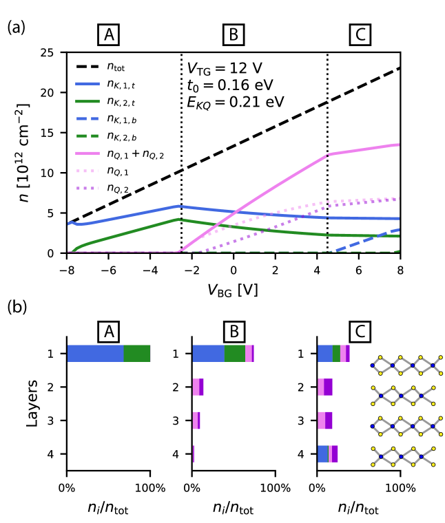
This model successfully captures the gate voltage dependence of the valley-specific densities and provide insights into the layer distribution of electron densities. In regime B, the model predicts an asymmetric density distribution across the layers, which results in a spin degeneracy lifting of valley states when , due to SOC [see dotted lines in Fig. 3(a)]. This prediction aligns with a detailed analysis of the FFT spectrum (see Supplementary Information), where we observe a splitting of the SdHO frequency corresponding to the residual density.
The experimentally observed splitting of the valley is notably less pronounced than predicted by our model. This discrepancy may arise from crystal field effects at the interface with the hBN dielectrics [23]. In the Supplementary Information, we account for the influence of hBN by introducing an on-site potential energy difference, , between the outer layers (which interface directly with hBN) and the inner layers. Incorporating this offset reduces the hybridization between the Q valleys of the outer and inner layers. This adjustment results in a more symmetric layer distribution of the valley electrons, thereby mitigating inversion symmetry breaking induced by the displacement field and leading to a weaker spin-orbit splitting. Consequently, the model’s prediction of spin-orbit splitting becomes more consistent with the experimental observations.
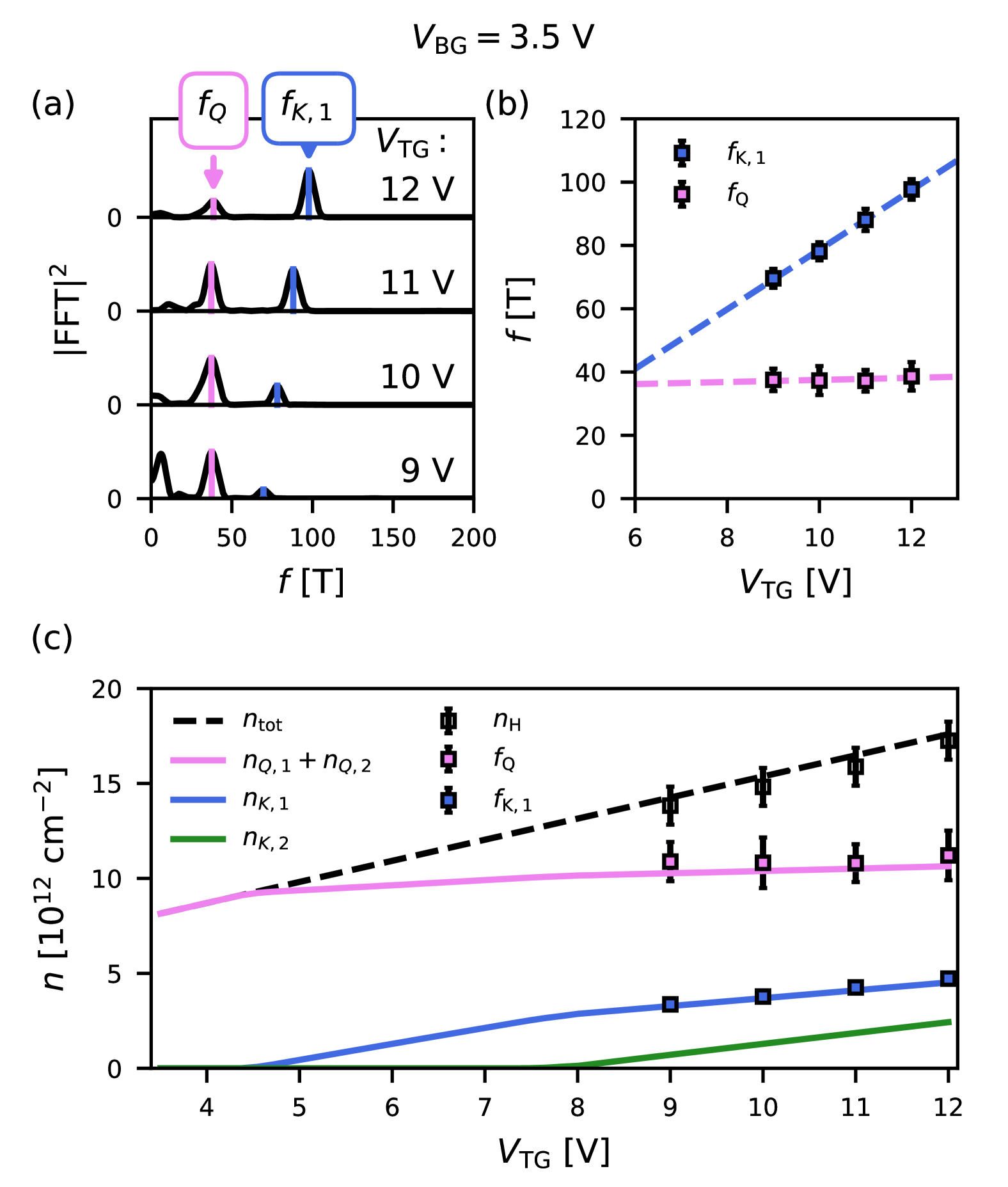
Next, we examine the effect of the top gate voltage, focusing on the densities in the and valley of the top layer. To track the top gate dependence of these densities, we present the FFT of at for various in Fig. 4(a). In this regime, the finite allows us to observe oscillations originating from both and valley states of the top layer without inducing charges in the valleys of the bottom layer. Figure 4(b) shows that the valley frequency of the top layer increases with , while the valley frequency is nearly constant due to interlayer screening. These data suggest that the top gate voltage induces a transition of the band edge from the valleys at low gate voltages to the valleys at higher voltages.
In Fig. 4(c), we compare valley densities predicted by the model (solid lines) with experimental densities (square markers), showing a good agreement. Due to high contact resistance, the low regime is experimentally inaccessible, so we rely on model predictions for this range. According to the model, at low bias (), the valley remains the only occupied band, confirming that the conduction band minimum in low-biased four-layer MoS2 is located at the point and demonstrating the presence of a gate-induced band edge transition.
Having established the relevance of the gate bias in determining the relative band alignment in multilayer MoS2, we extended our model to bilayer and three-layer systems (see Supplementary Information) to address discrepancies between experiments and DFT-calculated band structures. Using consistent model parameters, and , we successfully reproduce the experimental findings across multiple layers.
For biased bilayer MoS2, the model predicts that the valleys in top and bottom layers are occupied bands, while the valleys are not, as observed in Ref. [10]. In our earlier study on three-layer MoS2 [11], we observed electron transport predominantly through the valleys in the outer layers, although the band contributing to the electrons in the middle layer remained unidentified. Our model reveals the missing element in our previous work, showing that both and valleys were populated, as observed in the four-layer case.
III Conclusion
In conclusion, our study provides a comprehensive understanding of the gate-tunable band structure and valley occupation in four-layer MoS2 through a combination of magnetotransport experiments and a self-consistent hybrid tight-binding model. At low gate voltages, we confirm that the conduction band minimum is centered at the point, in line with theoretical expectations for multilayer MoS2. However, as the gate voltage increases, charge redistribution towards the layer closest to the positive gate electrode induces a transition of the band edge from the valleys to the valleys. By extending our model to bilayer and three-layer MoS2, we successfully bridge previous discrepancies between experimental observations [10, 11] and density functional theory predictions [12, 13, 14, 15, 16, 17], underscoring the importance of interlayer screening and layer-specific charge accumulation in determining valley occupation. These findings highlight the intricate interplay between the and valleys in multilayer MoS2, paving the way for future valleytronic and electronic applications that exploit layer-specific charge and valley control.
Acknowledgments
We thank Peter Märki, Thomas Bähler, as well as the FIRST staff for their technical support. We acknowledge support from the European Graphene Flagship Core 3 Project, Swiss National Science Foundation via NCCR Quantum Science, and H2020 European Research Council (ERC) Synergy Grant under Grant Agreement 95154. This work was supported by EPSRC Grants EP/S030719/1 and EP/V007033/1, and the Lloyd Register Foundation Nanotechnology Grant. Collaboration between ETH and the University of Manchester was supported by the International Science Partnerships Fund (UK). I.S. and X.L. acknowledge financial support from the University of Manchester’s Dean’s Doctoral Scholarship. I.R. gratefully acknowledges the support of CARA Fellowship and BA/Cara/Leverhulme Research Support Grant LTRSF24/100044. K.W. and T.T. acknowledge support from the JSPS KAKENHI (Grant Numbers 21H05233 and 23H02052) , the CREST (JPMJCR24A5), JST and World Premier International Research Center Initiative (WPI), MEXT, Japan.
References
- Kim et al. [2012] S. Kim, A. Konar, W.-S. Hwang, J. H. Lee, J. Lee, J. Yang, C. Jung, H. Kim, J.-B. Yoo, J.-Y. Choi, Y. W. Jin, S. Y. Lee, D. Jena, W. Choi, and K. Kim, High-mobility and low-power thin-film transistors based on multilayer MoS2 crystals, Nature Communications 3, 1011 (2012).
- Movva et al. [2015] H. C. P. Movva, A. Rai, S. Kang, K. Kim, B. Fallahazad, T. Taniguchi, K. Watanabe, E. Tutuc, and S. K. Banerjee, High-Mobility Holes in Dual-Gated WSe2 Field-Effect Transistors, ACS Nano 9, 10402 (2015).
- Sebastian et al. [2021] A. Sebastian, R. Pendurthi, T. H. Choudhury, J. M. Redwing, and S. Das, Benchmarking monolayer MoS2 and WS2 field-effect transistors, Nature Communications 12, 693 (2021).
- Wang et al. [2012] Q. H. Wang, K. Kalantar-Zadeh, A. Kis, J. N. Coleman, and M. S. Strano, Electronics and optoelectronics of two-dimensional transition metal dichalcogenides, Nature Nanotechnology 7, 699 (2012).
- Geim and Grigorieva [2013] A. K. Geim and I. V. Grigorieva, Van der waals heterostructures, Nature 499, 419 (2013).
- Kormányos et al. [2015] A. Kormányos, G. Burkard, M. Gmitra, J. Fabian, V. Zólyomi, N. D. Drummond, and V. Fal’ko, kp theory for two-dimensional transition metal dichalcogenide semiconductors, 2D Materials 2, 022001 (2015).
- Mak et al. [2010] K. F. Mak, C. Lee, J. Hone, J. Shan, and T. F. Heinz, Atomically Thin : A New Direct-Gap Semiconductor, Physical Review Letters 105, 136805 (2010).
- Splendiani et al. [2010] A. Splendiani, L. Sun, Y. Zhang, T. Li, J. Kim, C.-Y. Chim, G. Galli, and F. Wang, Emerging photoluminescence in monolayer MoS , Nano Letters 10, 1271 (2010).
- Pisoni et al. [2018] R. Pisoni, A. Kormányos, M. Brooks, Z. Lei, P. Back, M. Eich, H. Overweg, Y. Lee, P. Rickhaus, K. Watanabe, T. Taniguchi, A. Imamoglu, G. Burkard, T. Ihn, and K. Ensslin, Interactions and magnetotransport through spin-valley coupled landau levels in monolayer , Physical Review Letters 121, 247701 (2018).
- Pisoni et al. [2019] R. Pisoni, T. Davatz, K. Watanabe, T. Taniguchi, T. Ihn, and K. Ensslin, Absence of Interlayer Tunnel Coupling of -Valley Electrons in Bilayer , Physical Review Letters 123, 117702 (2019).
- Masseroni et al. [2021] M. Masseroni, T. Davatz, R. Pisoni, F. K. de Vries, P. Rickhaus, T. Taniguchi, K. Watanabe, V. Fal’ko, T. Ihn, and K. Ensslin, Electron transport in dual-gated three-layer , Physical Review Research 3, 023047 (2021).
- Mattheiss [1973] L. F. Mattheiss, Band structures of transition-metal-dichalcogenide layer compounds, Physical Review B 8, 3719 (1973).
- Li and Galli [2007] T. Li and G. Galli, Electronic Properties of MoS2 Nanoparticles, The Journal of Physical Chemistry C 111, 16192 (2007).
- Lebègue and Eriksson [2009] S. Lebègue and O. Eriksson, Electronic structure of two-dimensional crystals from ab initio theory, Physical Review B 79, 115409 (2009), publisher: American Physical Society.
- Ellis et al. [2011] J. K. Ellis, M. J. Lucero, and G. E. Scuseria, The indirect to direct band gap transition in multilayered MoS2 as predicted by screened hybrid density functional theory, Applied Physics Letters 99, 261908 (2011).
- Yun et al. [2012] W. S. Yun, S. W. Han, S. C. Hong, I. G. Kim, and J. D. Lee, Thickness and strain effects on electronic structures of transition metal dichalcogenides: 2H-MX2 semiconductors ( M = Mo, W; X = S, Se, Te), Physical Review B 85, 033305 (2012).
- Sun et al. [2016] Y. Sun, D. Wang, and Z. Shuai, Indirect-to-direct band gap crossover in few-layer transition metal dichalcogenides: A theoretical prediction, The Journal of Physical Chemistry C 120, 21866 (2016).
- Movva et al. [2018] H. C. Movva, T. Lovorn, B. Fallahazad, S. Larentis, K. Kim, T. Taniguchi, K. Watanabe, S. K. Banerjee, A. H. MacDonald, and E. Tutuc, Tunable - Valley Populations in Hole-Doped Trilayer , Physical Review Letters 120, 107703 (2018).
- Fallahazad et al. [2016] B. Fallahazad, H. C. P. Movva, K. Kim, S. Larentis, T. Taniguchi, K. Watanabe, S. K. Banerjee, and E. Tutuc, Shubnikov–de Haas Oscillations of High-Mobility Holes in Monolayer and Bilayer WSe2 : Landau Level Degeneracy, Effective Mass, and Negative Compressibility, Physical Review Letters 116, 086601 (2016).
- Larentis et al. [2018] S. Larentis, H. C. P. Movva, B. Fallahazad, K. Kim, A. Behroozi, T. Taniguchi, K. Watanabe, S. K. Banerjee, and E. Tutuc, Large effective mass and interaction-enhanced Zeeman splitting of -valley electrons in , Physical Review B 97, 201407 (2018).
- Masseroni et al. [2023] M. Masseroni, T. Qu, T. Taniguchi, K. Watanabe, T. Ihn, and K. Ensslin, Evidence of the coulomb gap in the density of states of , Phys. Rev. Res. 5, 013113 (2023).
- Rozhansky and Fal’ko [2024] I. Rozhansky and V. Fal’ko, Exchange-enhanced spin-orbit splitting and its density dependence for electrons in monolayer transition metal dichalcogenides, Phys. Rev. B 110, L161404 (2024).
- Rickhaus et al. [2019] P. Rickhaus, G. Zheng, J. L. Lado, Y. Lee, A. Kurzmann, M. Eich, R. Pisoni, C. Tong, R. Garreis, C. Gold, M. Masseroni, T. Taniguchi, K. Wantanabe, T. Ihn, and K. Ensslin, Gap Opening in Twisted Double Bilayer Graphene by Crystal Fields, Nano Letters 19, 8821 (2019).
Author contributions
M.M., T.I., K.E. conceived and designed the experiments. M.M. fabricated the device with inputs from T.I. and K.E.. M.M., performed the measurements with inputs from T.I and K.E.. M.M. and A.S. analyzed the experimental data with inputs from M.N., T.I., and K.E.. I.S. and V.F. developed the theoretical model with inputs from J.G.M., I.R., and X.L.. M.M. designed the figures with inputs from I.S.. T.T., K.W. supplied the hexagonal boron nitride. M.M wrote the manuscript with inputs from I.S., J.G.M. and I.R.. All the coauthors mentioned above read and commented on the manuscript. M.M. and I.S. contributed equally to this work.