Annealing behaviour of charge collection of neutron irradiated diodes from 8-inch p-type silicon wafers
Abstract
To face the higher levels of radiation due to the 10-fold increase in integrated luminosity during the High-Luminosity LHC, the CMS detector will replace the current Calorimeter Endcap (CE) using the High-Granularity Calorimeter (HGCAL) concept. The electromagnetic section as well as the high-radiation regions of the hadronic section of the CE (fluences above ) will be equipped with silicon pad sensors, covering a total area of 620 . Fluences up to and doses up to 2 MGy are expected considering an integrated luminosity of 3 . The whole CE will normally operate at -35°C in order to mitigate the effects of radiation damage.
The silicon sensors are processed on novel 8-inch p-type wafers with an active thickness of 300 µm, 200 µm and 120 µm and cut into hexagonal shapes for optimal use of the wafer area and tiling. With each main sensor several small sized test structures (e.g pad diodes) are hosted on the wafers, used for quality assurance and radiation hardness tests. In order to investigate the radiation-induced bulk damage, these diodes have been irradiated with neutrons at JSI (Jožef Stefan Institute, Ljubljana) to fluences between and .
The charge collection of the irradiated silicon diodes is determined through transient current technique (TCT) measurements. The study focuses on the isothermal annealing behaviour of the bulk material at 60°C. The results have been used to optimize the layout of the silicon modules in HGCAL and are being used to estimate the expected annealing effects of the silicon sensors during year-end technical stops and long HL-LHC shutdowns currently foreseen with a temperature around 0°C.
1 Introduction
The High-Luminosity Large Hadron Collider (HL-LHC) upgrade aims at enhancing the performance of the LHC, the most powerful particle accelerator in the world, to boost the potential for scientific discoveries starting from 2030. The project includes increasing the luminosity (and thus the collision rate) by a factor of five beyond the original LHC design specifications. The goal for the integrated luminosity is to increase it by a factor of ten. This poses significant challenges in terms of radiation tolerance and event pileup for the detectors [1, 2].
As part of the HL-LHC upgrade within the CMS Experiment [3], the current Calorimeter Endcap (CE) will be replaced, using the novel High Granularity Calorimeter (HGCAL) concept. It will consist of 47 sampling layers interleaved with absorber plates and will include nearly six million readout channels.
Silicon sensors were selected as active material for the majority of the CE upgrade due to their compactness, rapid signal formation, and adequate radiation hardness. At the HL-LHC, these silicon sensors will be subjected to hadron fluences ranging from approximately 1-MeV neutron-equivalents per square centimeter to after an integrated luminosity of 3000 . Around 620 of silicon sensors will cover the entire electromagnetic (CE-E) section and the high-radiation region of the hadronic (CE-H) section of the calorimeter. The silicon sensors are fabricated on 8-inch wafers and diced to form hexagonal shape for efficient use of the wafer area and tiling [4, 2].
In this paper, we report about three measurement campaigns focusing on isothermal annealing behaviour of the charge collection capability of the silicon bulk material using dedicated test structure diodes from 8-inch wafers, irradiated with neutrons up to . The campaigns were performed in 2021 and 2023 in two measurement setups. Section 2 gives an overview and detailed information about the samples used in each campaign. The measurement setups and techniques are described in section 3. An insight into the data analysis procedure is presented in section 4. The discussion on the systematic uncertainties is provided in section 5. The results and interpretation of the obtained data can be found in section 6. Finally, the summary and conclusions are given in section 7.
2 Samples
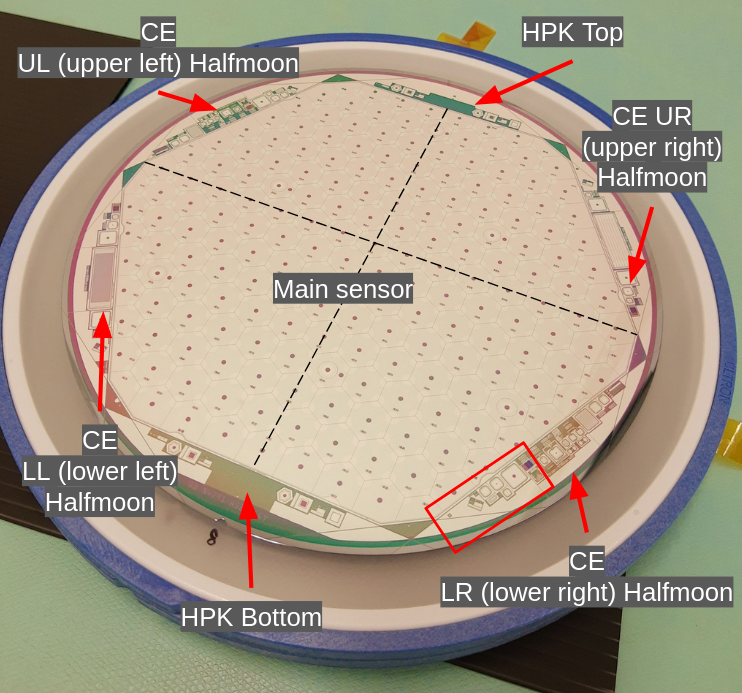
The silicon sensors to be used in the CMS Calorimeter Endcap upgrade consist of DC-coupled, planar, high resistivity (>3 kΩcm), p-type hexagonal silicon sensors with a crystal orientation of <100> produced on 8-inch circular wafers by Hamamatsu Photonics K.K222https://www.hamamatsu.com/eu/en.html (shown in figure 1) [2]. Sensors are produced in three different active thicknesses and two material types. 300 µm and 200 µm sensors are produced in the float zone (FZ) process, whereas 120 µm sensors are produced in the epitaxial (EPI) process on top of a handling wafer of 180 µm thickness. The remaining space left around the hexagonal main sensor (called "halfmoons") is used for the fabrication of small-sized test structures, which have an identical production process as the main sensor. The test structures include, among others, single diodes which can be used to investigate the bulk radiation hardness of the sensors. For the measurements presented here, square diodes with a side length of 5 mm are chosen. The main pad implant is surrounded by a guard ring.
In the following, results from three independent charge collection measurement campaigns are presented, performed in two different setups referred to as "TCT+ setup" and "Particulars setup"333https://particulars.si/index.php. The setups are described in detail in section 3. In the TCT+ setup, two measurement campaigns were performed - one in 2021 with CE version-1 prototype samples, irradiated to intermediate fluences ( to ) and one in early 2023 with CE version-2 prototype samples (and with additional version-1 prototype 120 µm samples), irradiated to higher fluences ( to ). The third campaign was performed in the Particulars setup in 2023, where CE pre-series samples, irradiated to higher fluences ( to ), were measured. Version-1 and version-2 prototypes and pre-series sensors represent different production rounds performed for the CE. The rounds mostly differ in terms of parameters regarding the oxide process. Typical variations in the bulk production process are known to be independent of the manufacturer’s oxide process, such that compatible performance in the charge collection measurements is expected. In each campaign, isothermal annealing studies were performed. Detailed information about the samples and annealing steps for each campaign is listed in tables 1, 2 and 3, respectively. All diodes were irradiated with neutrons at the Jožef Stefan Institute, Ljubljana, Slovenia [5]. In addition to the irradiated samples, each campaign included a set of unirradiated samples - one for each thickness - to serve as reference sensors.
| Sensor ID | Active | Fluence | Irradiation | Est. initial 60°C |
|---|---|---|---|---|
| thickness [µm] | [1015 neq/cm2] | time [min] | offset [min] | |
| 1002_LR | 300 | 0.65 | 7.4 | 1.0 |
| 1003_LR | 300 | 1.00 | 10.8 | 1.6 |
| 1102_LR | 300 | 1.50 | 16.2 | 2.4 |
| 2002_LR | 200 | 1.00 | 10.8 | 1.6 |
| 2003_LR | 200 | 1.50 | 16.2 | 2.4 |
| 2102_LR | 200 | 2.50 | 27.5 | 4.0 |
| 3008_LR | 120 | 1.50 | 16.2 | 2.4 |
| 3007_LR | 120 | 2.50 | 27.5 | 4.0 |
| 3003_LR | 120 | 10.00 | 108.0 | 14.2 |
| Annealing steps [min] | 10, 30, 90, 120 (all samples), | |||
| 260 (1003_LR, 2002_LR, 3008_LR, 3003_LR), | ||||
| 300 (1002_LR, 1102_LR, 2003_LR, 2102_LR, 3007_LR). | ||||
| Sensor ID | Active | Fluence | Irradiation | Est. initial 60°C |
|---|---|---|---|---|
| thickness [µm] | [1015 neq/cm2] | time [min] | offset [min] | |
| N4791_11_LR | 300 | 1.50 | 16.2 | 2.4 |
| N4791_12_LL | 300 | 2.00 | 21.8 | 3.2 |
| N4791_13_LR | 300 | 3.00 | 32.6 | 4.7 |
| N4792_10_LR | 200 | 2.00 | 21.8 | 3.2 |
| N4792_11_LL | 200 | 4.00 | 43.3 | 6.1 |
| N4792_12_LR | 200 | 5.50 | 59.5 | 8.1 |
| N4789_10_LL | 120 | 5.50 | 59.5 | 8.1 |
| N4789_12_UL | 120 | 10.00 | 108.0 | 14.2 |
| N4789_13_UR | 120 | 14.00 | 151.2 | 19.6 |
| 3008_UR | 120 | 1.50 | 16.2 | 2.4 |
| 3007_UR | 120 | 2.50 | 27.5 | 4.0 |
| 3003_UR | 120 | 10.00 | 108.0 | 14.2 |
| Annealing steps [min] | 0, 90. | |||
| Sensor ID | Active | Fluence | Irradiation | Est. initial 60°C |
|---|---|---|---|---|
| thickness [µm] | [1015 neq/cm2] | time [min] | offset [min] | |
| N8738_1 LL1 | 300 | 2.00 | 21.8 | 3.2 |
| N8738_2 LR | 300 | 4.00 | 43.3 | 6.1 |
| N8740_1 LL1 | 200 | 4.00 | 43.3 | 6.1 |
| N8740_2 LL1 | 200 | 6.00 | 64.9 | 8.8 |
| N8740_3 LL2 | 200 | 8.00 | 86.8 | 11.6 |
| N8737_3 UL | 120 | 6.00 | 64.9 | 8.8 |
| N8737_2 LL1 | 120 | 15.00 | 161.8 | 20.9 |
| Annealing steps [min] | 0, 30, 55, 85, 120, 150, 200, 275, 365, 510. | |||
During the irradiation, the diodes are exposed to temperatures reaching up to ()°C. This is taken into account as in-reactor annealing when determining the total annealing times and its uncertainty for the individual samples. The temperature during the irradiation is assumed to increase from the minimum of 25°C to the maximum temperature after 30 min where it stabilizes. The temperature increase and decrease is assumed to follow exponential functions, with distinct time constants for each phase [6]. Based on this information, the irradiation time, listed in tables 1, 2 and 3, is converted to an equivalent annealing time at 60°C (using the so-called Hamburg model derived in [7, 8]) and included in the tables as estimated initial 60°C offset. The estimated annealing times have an uncertainty which is displayed in the figures as error bars.
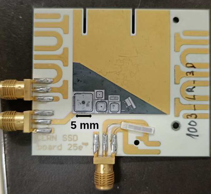
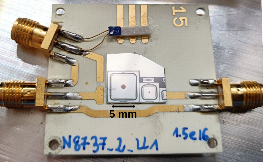
After the irradiation, samples are mounted on a printed circuit board (PCB). The diode is wire-bonded to a SubMiniature version A (SMA) connector enabling appropriate connection to the measurement circuit through which it is grounded. The diode’s guard ring is grounded. The high voltage is applied to the diode’s backside. In order to control the temperature of the diode, in the following referred to as device under test (DUT), during the measurement, a PT1000 resistor is glued close to the DUT. In the 2021 TCT+ campaign, the PCB 25e layout, shown in figure 2(a), was used. Such a large PCB size was used to avoid further dicing the pre-diced triangles of the halfmoons containing the DUT. However, it was found non-optimal for homogeneous cooling of the PCB area, especially below the DUT. For the next two campaigns (both 2023 campaigns), a smaller PCB layout (PCB 15, shown in figure 2(b)) was chosen to improve homogeneity of the temperature across the DUT. To fit the size of PCB 15, the silicon triangles had to be diced, which was performed using a diamond scribe. This posed the risk of damaging the diode intended for testing during the cutting especially since the silicon crystal orientation and the diode orientation differ by 30 degrees, as can be seen in figure 1.
Between measurements, the samples were annealed in several steps. The annealing is performed in a dedicated oven preheated to a temperature of 60°C. For the annealing, the samples are placed on preheated copper blocks for good thermal contact. The temperature was monitored every second using a PT1000 resistor attached to one of the PCBs. The estimated initial offset is added to the additional annealing steps resulting in the total annealing time. The additional annealing steps are listed in the bottom row of tables 1, 2 and 3. Except during annealing or measurement, the samples are stored in a freezer to avoid excess annealing.
3 Measurement setups
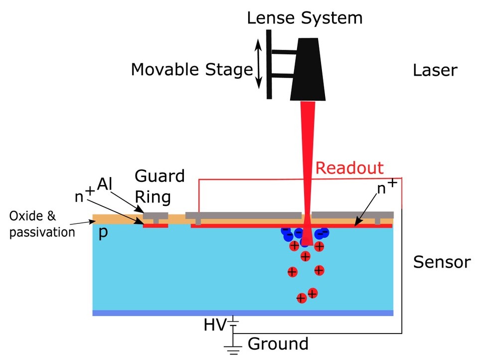
The ability to collect charge by the silicon sensors can be measured using the Transient Current Technique (TCT) [9]. In this method, a laser pulse generates electron-hole pairs in the silicon bulk. As an external bias voltage is applied to the silicon diode, the generated charge carriers drift towards the corresponding electrodes. The induced current is recorded as a function of time.
For all measurements reported in this publication, the DUTs are reverse-biased, with high voltage applied to the back side bulk contact. The readout is connected to an oscilloscope via an amplifier. Laser light of 1064 nm wavelength (infra-red) is injected from the front side of the DUT (IR-top TCT) directed at a 1mm-diameter hole in centre of the metal contact layer of the diode. The schematic principle of the top-TCT measurement is shown in figure 3. In the 2021 TCT+ campaign, a laser intensity equivalent to 33 MIPs (minimum ionizing particles) was used. For the 2023 TCT+ and Particulars campaigns, the intensity was increased to 40 MIPs in order to enhance the signal for highly irradiated diodes. In the previous studies ([2, 10]), it was shown that an IR light signal equivalent to multiple MIPs gives compatible results to single-MIP measurements using a radioactive source. The measurements are conducted with the DUT cooled down to -20°C in order to reduce the leakage current of the irradiated sensors.
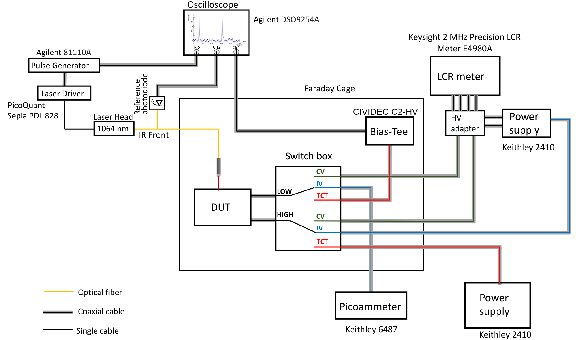
Both setups offer the capability for electrical characterization in addition to TCT measurements, enabling the measurement of leakage current (IV) and capacitance (CV) as a function of the reverse bias voltage. The diagram of the TCT+ setup is shown in figure 4. More details about IV and CV measurements can be found in [6].
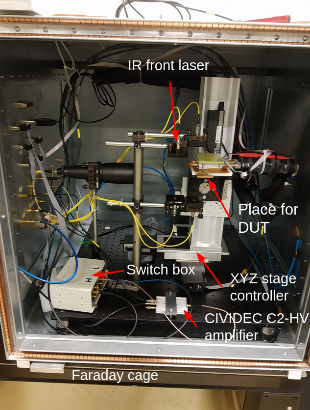
While both setups serve the same purpose, they differ in certain details: in the TCT+ setup (figure 5(a)), the DUT attached to a PCB is mounted on a copper holder, which is cooled by a Peltier element connected to a chiller. To adjust the laser focus and position of the DUT, an XYZ stage is used. The stage moves the copper holder, while the laser is in a fixed position. The measured signal is amplified by a CIVIDEC C2-HV amplifier, a general purpose broadband current amplifier with integrated bias-T and an amplification of 43 dB [13]. A switch box, visible in figure 5(a), changes the measurement type between TCT, IV and CV. The major part of the setup is placed inside a Faraday cage and flushed with dry air to avoid condensation and frost. Additionally, the setup is equipped with a reference photodiode. The laser light is split into two beams: 90% of the intensity is directed to the DUT, while 10% is sent to the reference photodiode. This allows for monitoring both the presence and intensity of the laser light.
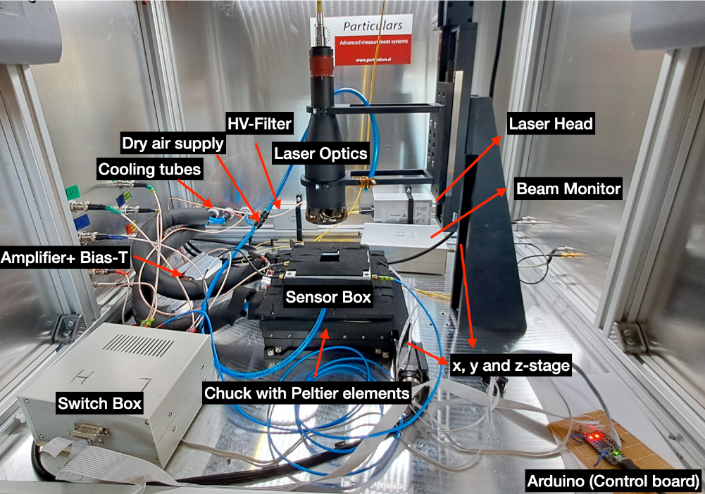
In the Particulars setup (figure 5(b)), the DUT attached to a PCB is also mounted on a copper plate. It is enclosed in a sensor box, which is then placed on a chuck equipped with Peltier elements cooled with a chiller. The XY stage present in this setup controls the position of the DUT, while the Z stage independently moves the laser up and down, varying the focus position of the laser beam. The amplifier used in this setup is a wide band current amplifier with an amplification of 53 dB [14]. The switch box plays the same role as in the TCT+ setup. The main setup part, visible in figure 5(b), is also placed inside a Faraday cage. A dry air supply flushes both the Faraday cage and the sensor box. The schematic of the Particulars setup is equivalent to the TCT+ setup schematic, shown in figure 4, except for the brand of the amplifier, laser head, laser driver and pulse generator (all supplied by Particulars). Like the TCT+ setup, the Particulars setup employs a photodiode as beam monitor. However, the laser intensity is evenly split, with 50% directed towards the DUT and 50% towards the photodiode. Both the beam monitor and the laser head are placed inside the Faraday cage, which also contains an HV filter (to remove the noise in the HV line coming from the power supply) and external bias-T, which are both in the TCT+ circuit between the power supply and the sensor.
4 Data analysis procedure
Charge collection
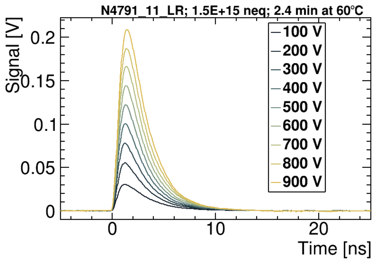
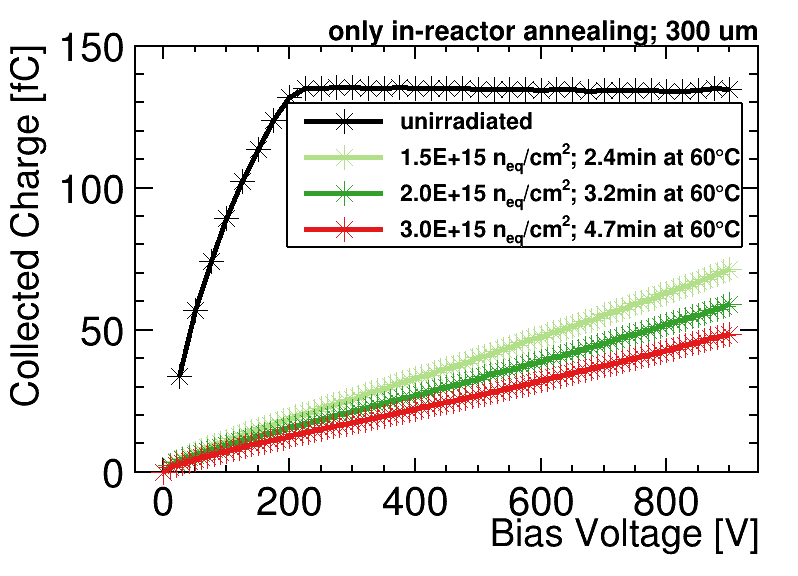
To determine the charge collection value, the TCT signal is measured and recorded. The transient current pulse is converted into a voltage pulse through the input impedance (50 Ω) of the amplifier. Figure 6(a) displays an example of TCT signals obtained during the 2023 TCT+ campaign from an irradiated diode at various bias voltages up to the chosen measurement limit of 900 V. This limit was chosen to reduce the risk of destructive discharges. The signal’s amplitude correlates with the applied bias voltage on the DUT. In both TCT+ setup campaigns, the waveform measured at a particular bias voltage utilizes an average waveform, representing an average of 1000 samples. For the 2023 Particulars campaign, 300 averaged waveforms are captured for each bias voltage, with a single waveform averaging 50 samples, representing 15 000 samples.
The collected charge value at a specific bias voltage is calculated as the integral of the TCT signal waveform (for a time window at 0 ns to 25 ns) divided by the amplifier gain. An example of the charge collection vs. bias voltage dependence is depicted in figure 6(b). After this initial data processing, the charge collection at a selected bias voltage can be analysed as a function of fluence or annealing time.
Saturation voltage
In figure 6(b), it is clearly visible that the charge collection for unirradiated samples saturates after reaching a certain voltage. This point is identified as the depletion voltage, which is determined using the same method as in CV measurements: by fitting the rising part of the curve and the plateau region, with the intersection point of these two fits representing the extracted depletion voltage. However, for irradiated sensors, extracting the depletion voltage is significantly more challenging. It is noteworthy that we distinguish "saturation voltage" from "depletion voltage". This distinction arises from our observation that the concept of depletion voltage no longer holds true for irradiated devices since its value depends on the measurement frequency (for CV measurement) and the temperature [6].
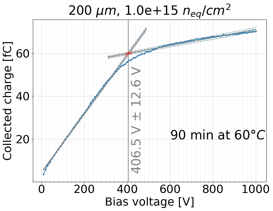
For the low fluences and thin sensors covered in this study, where the saturation voltage lies well below the measurement limit of 900 V, extracting the saturation voltage from charge collection measurements becomes feasible. An example is shown in figure 7. Unlike in unirradiated sensors, the plateau region is absent in irradiated sensors due to the occurrence of charge trapping, of which the probability decreases with increasing bias voltage and hence the electric field. This results in an increase in charge beyond the saturation voltage. Each part is fitted with a linear fit, and the intersection point is identified as the extracted saturation voltage. If the second rising part is not reached within the measured voltage range or the two slopes become too similar, it becomes impossible to extract the saturation voltage (as visible in figure 6(b) for the irradiated samples).
5 Systematic uncertainties
Systematic uncertainties of charge collection were determined by considering five factors present during the campaigns, with two being the most significant: the laser and the temperature stability. Long-term measurements of the laser intensity in the TCT+ setup, recorded by the reference photodiode (ref. section 3), revealed a small instability over time. To account for this instability, all the charge collection results obtained using the TCT+ setup in this study were calibrated by normalizing the laser intensity during the measurements to the intensity recorded during a reference measurement with a 300 µm unirradiated diode.
Next, we considered the uncertainty in the sensor’s temperature during measurements, which affects the laser absorption in the silicon.
In the TCT+ setup, the temperature is controlled within .
The 25e PCB layout used for the 2021 TCT+ campaign was larger than the copper holder in the setup, leading to temperature inhomogeneity across the PCB.
Additionally, it was observed, using an infra-red camera, that the SMA connectors were warmer than the middle part of the PCB, where the diode was located.
The PT1000 sensor’s proximity to the SMA connector (ref. figure 2(a)) resulted in higher temperature readings.
This suggests that the diode could have been cooled more than intended.
The laser band-to-band absorption () depends on the temperature as follows [15, 16, 17]:
| (5.1) |
where is the nominal temperature for the absorption coefficient data (-20°C in our case) and is the temperature coefficient. Based on the infra-red images of the setup, we assume that the sensor temperature during the 2021 TCT+ campaign was between -24°C and -19°C. This translates to an uncertainty in charge collection due to temperature change of +6.1% and -1.6%. For the 2023 TCT+ campaign, smaller PCBs were used (ref. figure 2(b)) which allows improved temperature control. However, since the DUTs were already mounted to the PCBs, it was not possible to place a PT1000 directly onto them without the risk of damaging the DUT in the soldering process and uncontrolled annealing. Instead, a PT1000 was attached to an additional copper sheet placed between the copper holder of the TCT+ setup and the PCB. This increased the uncertainty of the temperature measurement. For this campaign, the DUT’s temperature is assumed to be between -25°C and -18°C, resulting in an uncertainty in the charge collection due to temperature of +7.6% and -3.2%.
There are two additional charge collection uncertainties considered for the TCT+ setup. As the setup, during both campaigns, was also used by other users, it required everyday calibration. This was achieved by measuring the charge collection of the 300 µm unirradiated diode (as a reference) at +20°C at the start of each measurement day and adjusting the laser intensity to maintain consistent charge collection values. The variations in charge collection resulted in a 0.78% uncertainty for 2021 TCT+ campaign and a 0.61% uncertainty for 2023 TCT+ campaign. The second factor concerns the replacement of the amplifier in the setup on one occasion during 2021 TCT+ campaign and two occasions during 2023 TCT+ campaign, due to their failures. After each amplifier replacement, the laser intensity was recalibrated in the same manner as during the daily calibration. The variations in charge collection resulting from the amplifier replacements introduced a 0.20% uncertainty for 2021 TCT+ campaign and 0.61% uncertainty for 2023 TCT+ campaign.
All uncertainties were combined in quadrature, resulting in a total charge collection uncertainty of +6.7% and -3.1% for the 2021 TCT+ campaign and +9.6% and -5.1% for the 2023 TCT+ campaign.
The Particulars setup was exclusively used for this measurement campaign, with no other users. A temperature uncertainty of the small PCB 15 has to be considered (1°C), as well as an uncertainty regarding the laser stability. To monitor this, a reference 300 µm unirradiated diode was measured daily. It was found that environmental temperature variations slightly influence the laser intensity, as well as the temperature stability of the DUT. To account for this, an overall charge collection uncertainty of 5% was estimated.
The last contributing factor to the charge collection uncertainty is the fit uncertainty of the Gaussian fit applied to the charge collection distribution of the 300 recorded events, of which the most probable value defines the CC for each measured voltage.
To assess the uncertainty in annealing time, we first account for the uncertainty in the estimated initial 60°C offset, which is derived by considering the full impact of the reactor temperature uncertainty. These effects become more pronounced for longer irradiation times. Considering the high total annealing times - up to 500 min - done in this campaign, the impact of the uncertainty of the in-reactor annealing becomes negligible. Next, for the individual annealing steps, we assign a 0.5°C uncertainty in the temperature measurement, based on the temperature recordings. The primary factor contributing to this uncertainty is the potential for small temperature variations between different PCBs. The uncertainty in the time measurement itself is negligible.
The uncertainty on the fluence is consistently 10% for all fluences.
6 Results
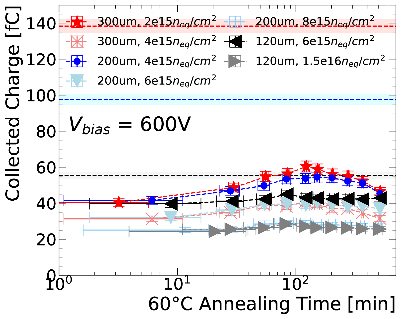
The data collected throughout different campaigns are used to characterize the behavior of the charge collection (ref. section 4) over a broad range of fluence. Figure 8 depicts the charge collection behavior at a bias voltage of 600 V after approximately 90-minute annealing at 60°C for all three sensor thicknesses. In figure 8, only the charge collection data from the two 2023 campaigns are presented, while the results from the 2021 TCT+ campaign are omitted since a different in laser intensity was used (33 MIPs equivalent vs. 40). The horizontal dotted lines represent the charge collection values for unirradiated sensors, with red indicating 300 µm, blue representing 200 µm, and black representing 120 µm. The trend reveals a decrease in collected charge as fluence increases, consistently observed across all three thickness variations. The collected charge values demonstrate agreement within the margins of uncertainty across different campaigns.
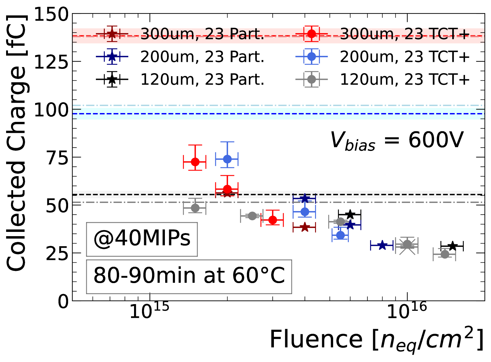
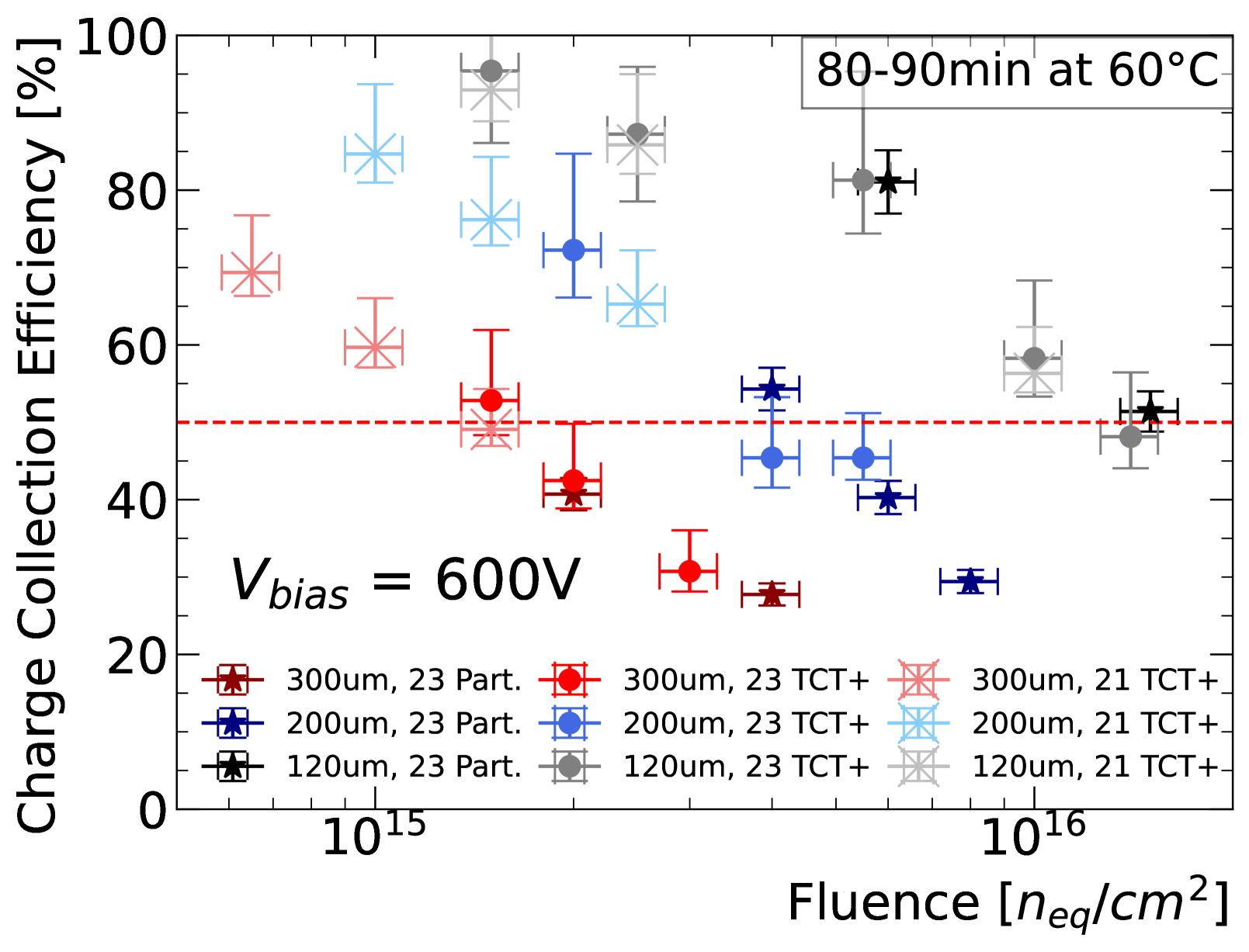
In figure 8, the charge collection efficiency (CCE), defined as the charge collection of an irradiated sample divided by the charge collection of the non-irradiated reference sensors, across all three campaigns is depicted. Once more, a distinct trend emerges: as fluence increases, the charge collection efficiency decreases across all thickness variations. The data collected from different campaigns and studies on earlier CE prototypes at lower fluences [18] exhibit agreement within the margins of uncertainty. At a fixed fluence, the 300 µm samples demonstrate the lowest charge collection efficiency, whereas the 120 µm samples exhibit the highest. This indicates their superior radiation hardness, rendering them suitable for deployment in the highest radiation regions of the CE. Specifically, for 600 V, the 300 µm samples achieve 50% charge collection efficiency up to a fluence of , the 200 µm samples up to , and the 120 µm samples up to . At a fluence of , the 120 µm samples still have nearly 100% efficiency.
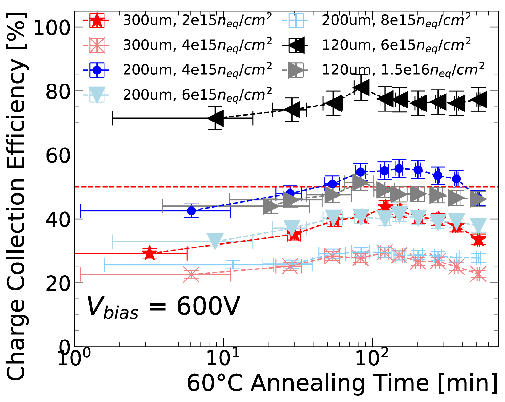
Taking a closer look at the dependence of the charge collection on annealing time, we focus on the 2023 Particulars dataset, depicted in figure 9, where annealing was performed in 10 steps up to 500 min. A visible increase in collected charge (figure 9) and efficiency of collected charge (figure 9) is observed for all samples during the region dominated by beneficial annealing. The maximum is reached at around 120 minutes for float zone samples and around 85 minutes for epitaxial samples followed by a decrease into region dominated by reverse annealing. These findings align with previous CC studies on p-type sensors [19, 20] and with the corresponding findings from CV measurements [6].
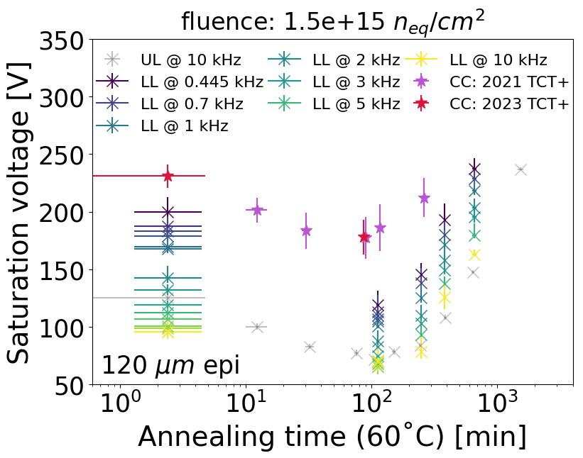
In previous studies [6], the saturation voltage (ref. section 4) extracted from capacitance versus bias voltage (CV) measurements, as a function of annealing time, was used as an input to the Hamburg model. However, the saturation voltage obtained from CV measurements is well known for its sensitivity to both frequency and temperature [21, 6]. To mitigate this dependency, we use charge collection as an independent alternative approach. Figure 10 illustrates a comparison between the depletion voltage extracted from CV and charge collection measurements, using a sample with the following properties: 120 µm thickness, irradiated to . The charge collection was measured during two campaigns: 2021 TCT+ and 2023 TCT+.
It is evident that, as the CV frequency increases, the extracted saturation voltage decreases. Moreover, the saturation voltage extracted from charge collection is higher compared to those obtained from CV with the lowest CV frequency being 445 Hz. This poses a challenge for thicker and highly irradiated sensors, where the saturation voltage is correspondingly higher. If the saturation voltage exceeds 900 V, it becomes infeasible to measure it using the CC method with the mentioned bias voltage limitation. However, the CC method is unaffected by measurement settings such as the frequency choice of the CV measurement, which is considered an advantage. It was shown in this study, for the temperature range -30°C to -15°C, that the saturation voltage for irradiated samples extracted from charge collection measurements stays constant within 0.1%.
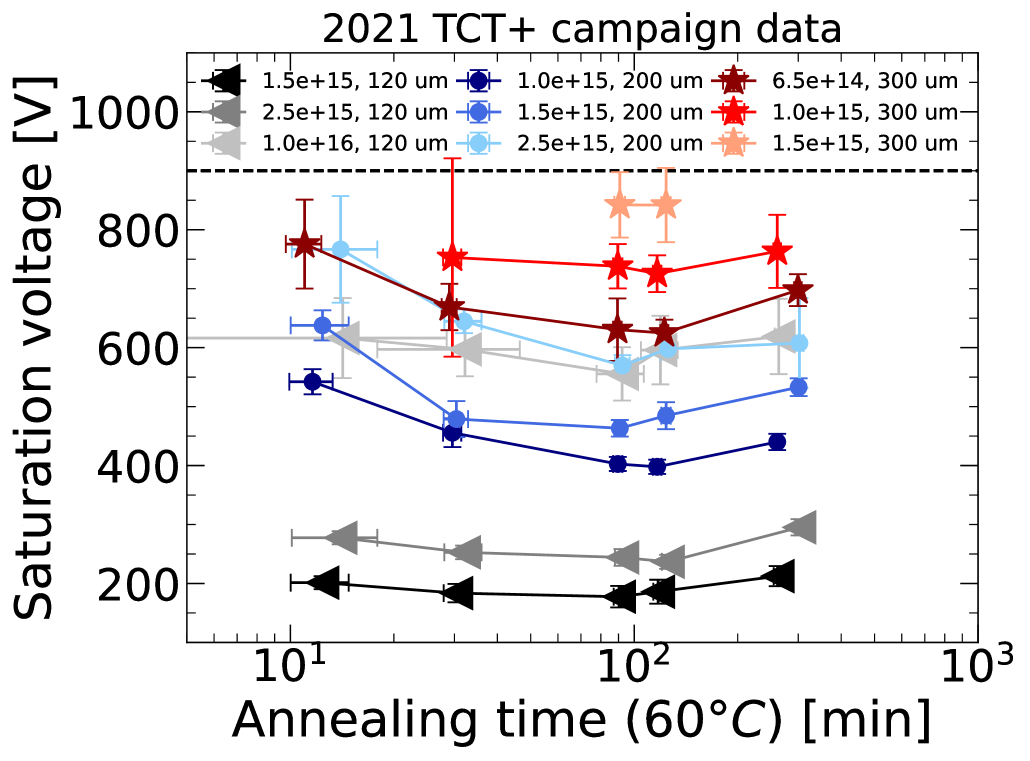
The extraction of the saturation voltage from charge collection data is feasible for samples where the saturation voltage is well below the measurement limit of 900 V which is true for the thin samples and low fluence 300 µm sample for the TCT+ 2021 campaign. The extracted saturation voltages are presented in figure 11. The minimum saturation voltage is observed between 90 and 120 minutes, consistent with results from CV measurements [6]. The results obtained from the measurement of the saturation voltage with different methods (CV, CC), frequencies (CV) and temperature can be used as inputs to the Hamburg model [7]. Such study could provide further insight on the characteristics of these sensors and on the differences of the methods used. However, such study would benefit from extending the annealing campaign results to fluences which are lower than the ones reported here. Hence it is beyond the scope of this paper.
7 Conclusions
The charge collection annealing behaviour of silicon diodes from 8-inch p-type wafers from the CE prototypes and pre-series phases is presented for a large fluence range. The combined results from three charge collection campaigns not only validate the new Particulars setup but also confirm that the bulk material of diodes from different CE manufacturing phases exhibit consistent behavior, as expected.
The results obtained in this study provide valuable input for optimizing the CE detector layout. Although thick sensors have a lower radiation tolerance, they benefit from an initially higher signal-to-noise ratio. Based on the results hereby reported, on the measurements of the leakage current [6] and on the expected performance of the front-end readout chip to be used in HGCAL [22], one can extend the usage of thicker sensors in higher fluence regions. With respect to the baseline [2] 200 µm are expected to be subject to fluences up to (instead of ) and 300 µm to fluences up to (instead of ) after 3.0 .
The cooling scheme used for the CE will ensure the operation at -35°C and never exceeding (-30°C). During the long shutdown periods it will be warmed up to approximately 0°C. This study supports the case that the silicon sensors will not enter the reverse annealing-dominated region significantly during the CE’s operational lifetime. Our findings show that the charge collection behavior of the novel 8-inch material with respect to annealing time reaches its maximum increase at around 120 minutes for float zone material and around 85 minutes for epitaxial material at 60°C. These results align with CV measurements and other studies on 6-inch p-type sensors, indicating that the CE 8-inch sensors will not experience significant reverse annealing until the end of HL-LHC if we apply the Hamburg model with the parameters values derived in [7], which allows extrapolating down to low temperature.
The presented dataset is currently being extended with an annealing campaign at additional temperatures (6.5°C, 20°C, 30°C, 40°C, 60°C) and annealing steps. Due to the slower annealing at the lower temperatures, results are expected in 2025/2026. This approach will enable to perform the Hamburg model fit at various annealing temperatures and extract for the first time scaling factors between the extracted parameters for the 8-inch p-type material. Consequently, it will be possible to predict the annealing behavior of CE silicon sensors at 0°C with better accuracy as using the current Hamburg model and establish appropriate CE operating conditions.
Acknowledgments
We thank the CERN EP-DT SSD group for providing the TCT+ setup to perform the measurements described in this publication, in particular Michael Moll, Ruddy Costanzi, Esteban Curras Rivera, Marcos Fernandez Garcia and Moritz Wiehe. Futhermore we thank Dana Groner and Ruddy Costanzi for help in upgrading the Particulars setup. Moreover, we thank the CERN EP R&D programme for funding the Particulars setup and the CMS HGCAL silicon sensor group for the discussions about the results presented here. We are grateful for feedback and suggestions from Rachel Yohay, Ronald Lipton, Pedro Silva and Philippe Bloch. This work has been sponsored by the Wolfgang Gentner Programme of the German Federal Ministry of Education and Research (grant no. 13E18CHA). This work has been supported by the Alexander-von-Humboldt-Stiftung.
References
- [1] G. Apollinari et al., High-Luminosity Large Hadron Collider (HL-LHC): Technical Design Report V. 0.1, CERN Yellow Reports: Monographs, CERN, Geneva (2017), 10.23731/CYRM-2017-004.
- [2] CMS collaboration, The Phase-2 Upgrade of the CMS Endcap Calorimeter, Tech. Rep. CERN-LHCC-2017-023, CMS-TDR-019, CERN, Geneva (2017), DOI.
- [3] CMS Collaboration, The CMS experiment at the CERN LHC, Journal of Instrumentation 3 (2008) S08004.
- [4] CMS HGCAL collaboration, Neutron irradiation and electrical characterisation of the first 8” silicon pad sensor prototypes for the CMS calorimeter endcap upgrade, Journal of Instrumentation 18 (2023) P08024.
- [5] V. Dimic, Reactor TRIGA at the J. Stefan institute in Ljubljana, Reaktor TRIGA Instituta “Jozef Stefan” v Ljubljani, Institut za Nuklearne Nauke Boris Kidric, Yugoslavia (1978).
- [6] J. Kieseler et al., Isothermal annealing of radiation defects in silicon bulk material of diodes from 8” silicon wafers, Journal of Instrumentation 18 (2023) P09010.
- [7] M. Moll, Radiation damage in silicon particle detectors: Microscopic defects and macroscopic properties, Ph.D. thesis, Hamburg U., 1999. https://inspirehep.net/literature/513308.
- [8] M. Moll, Displacement damage in silicon detectors for high energy physics, IEEE Trans. Nucl. Sci. 65 (2018) 1561.
- [9] G. Kramberger, Signal development in irradiated silicon detectors, Ph.D. thesis, Ljubljana U., 2001. http://cds.cern.ch/record/1390490.
- [10] E.C. Rivera, Advanced silicon sensors for future collider experiments, Ph.D. thesis, Cantabria U., Santander, 2017. https://cds.cern.ch/record/2291517.
- [11] L. Diehl, Investigation of Silicon Sensors Suitable for Collider Experiments in High Luminosity Environments, Ph.D. thesis, Albert Ludwigs Universität Freiburg, 2022. https://doi.org/10.6094/UNIFR/228617.
- [12] O. Kałuzińska, Silicon sensor characterisation and radiation hardness qualification for the CMS Endcap Calorimeter Upgrade for the High-Luminosity LHC, Master’s thesis, Wroclaw Tech. U., 2022, https://cds.cern.ch/record/2815709.
- [13] Cividec instrumentation, “C2-HV BROADBAND AMPLIFIER, 2 GHz, 40 dB.” https://cividec.at/electronics-C2-HV.html.
- [14] Particulars, Advanced Measurement Systems, “amplifiers.” https://particulars.si/products.php?prod=amplifiers.html.
- [15] C. Schinke et al., Uncertainty analysis for the coefficient of band-to-band absorption of crystalline silicon, AIP Advances 5 (2015) 067168.
- [16] M.A. Green, Self-consistent optical parameters of intrinsic silicon at 300k including temperature coefficients, Solar Energy Materials and Solar Cells 92 (2008) 1305.
- [17] K.G. Svantesson and N.G. Nilsson, Determination of the temperature dependence of the free carrier and interband absorption in silicon at 1.06m, Journal of Physics C: Solid State Physics 12 (1979) 3837.
- [18] N. Akchurin et al., Charge collection and electrical characterization of neutron irradiated silicon pad detectors for the cms high granularity calorimeter, Journal of Instrumentation 15 (2020) P09031.
- [19] L. Diehl et al., Annealing studies on irradiated p-type silicon strip sensors designed for the atlas phase ii tracking detector, RAD Association Journal 3 (2018) .
- [20] W. Adam et al., Experimental study of different silicon sensor options for the upgrade of the cms outer tracker, Journal of Instrumentation 15 (2020) P04017.
- [21] D. Campbell et al., Frequency and temperature dependence of the depletion voltage from cv measurements for irradiated si detectors, Nuclear Instruments and Methods in Physics Research Section A: Accelerators, Spectrometers, Detectors and Associated Equipment 492 (2002) 402.
- [22] F. Bouyjou et al., HGCROC3: the front-end readout ASIC for the CMS High Granularity Calorimeter, Journal of Instrumentation 17 (2022) C03015.