A two-dimensional semiconductor-semimetal drag hybrid
Abstract
Lateral charge transport of a two-dimensional (2D) electronic system can be much influenced by feeding a current into another closely spaced 2D conductor, known as the Coulomb drag phenomenon – a powerful probe of electron-electron interactions and collective excitations. Yet the materials compatible for such investigations remain limited to date. Especially, gapped 2D semiconductors with inherently large correlations over a broad gate range have been rarely accessible at low temperatures. Here, we show the emergence of a large drag response (drag resistance at the order of k, with a passive-to-active drag ratio up to 0.6) in a semiconductor-semimetal hybrid, realized in a graphene-MoS2 heterostructure isolated by an ultrathin 3 nm hexagonal boron nitride (h-BN) dielectric. We observe a crossover of - to -dependence of , separated by a characteristic temperature ( being the interlayer distance), in echo with the presence of a metal-insulator transition in the semiconducting MoS2. Interestingly, the current nanostructure allows the decoupling of intralayer interaction-driven drag response by varying density in one layer with that in the other layer kept constant. A large Wigner–Seitz radius ( 10 within the density range of 1 to 4) in the massive Schrödinger carriers in MoS2 is thus identified to dominate the quadratic dependence of total carriers in the drag system, while the massless Dirac carriers in graphene induce negligible drag responses as a function of carrier density. Our findings establish semiconductor-semimetal hybrid as a platform for studying unique interaction physics in Coulomb drag systems.
1 Shenyang National Laboratory for Materials Science, Institute of Metal Research, Chinese Academy of Sciences, Shenyang 110016, China
2 School of Material Science and Engineering, University of Science and Technology of China, Anhui 230026, China
3 Liaoning Academy of Materials, Shenyang 110167, P. R. China
4 State Key Laboratory of Quantum Optics Technologies and Devices, Institute of Optoelectronics, Shanxi University, Taiyuan 030006, P. R. China
5 Collaborative Innovation Center of Extreme Optics, Shanxi University, Taiyuan 030006, P. R. China
6 Research Center for Electronic and Optical Materials, National Institute for Materials Science, 1-1 Namiki, Tsukuba 305-0044, Japan
7 Research Center for Materials Nanoarchitectonics, National Institute for Materials Science, 1-1 Namiki, Tsukuba 305-0044, Japan
Corresponding to: wcren@imr.ac.cn, vitto.han@gmail.com, siwenzhao0126@gmail.com
Introduction
In two closely spaced low dimensional conductors, charge carriers driving in one active layer is often observed to induce drag characteristics in another passive layer, yielding a current or voltage in the latter. Such effects offer a fundamental yet direct probe for electronic momentum and/or energy exchange via long range Coulomb interactions, as well as many-body physics beyond single-particle transport[1]. Indeed, Coulomb drag phenomena have been extensively manifested in different regimes, including quantum wells or graphene separated with large distance in the weak coupling limit [2, 3], and excitonic condensation when interlayer charge carriers are matched in the quantum Hall limit [4, 5, 6, 7, 8, 9, 10, 11, 12]. More recently, emerging physical phenomena are also reported in exotic drag between graphene and superconductors, topological insulators, 1D-1D Luttinger liquid, quantum dots and mixed dimensional electrons[13, 14, 15, 16, 17, 18].
Among those reported, gapped two-dimensional (2D) semiconductors, with inherently large correlations in the massive carriers, have been a missing piece in the jigsaw puzzle of various drag regimes. Especially, a peculiar family of massive-massless double layers has remained largely unvisited. Taking the Wigner–Seitz radius (strong correlation when > 10) as a measure of interaction strength in 2D electron systems, massless Dirac fermions in monolayer graphene has a density-independent value of 0.7 - 0.8[19, 20]. Meanwhile, in bilayer graphene and conventional 2D electron gases in quantum wells, Fermi surfaces are well defined and is sufficiently large only when carrier density is remained ultra low (< ), which is manifested in such as an unconventional negative frictional drag in the vicinity of charge neutral in double graphene bilayers[21, 22]. Gapped 2D semiconductors, the transition metal dichalcogenides (TMDs) for instance, host strong tunable Coulomb interactions with 10 across a broad gate range[23, 24]. The interplay of these massive interacting Schrödinger fermions with massless Dirac fermions in the Coulomb drag paradigm is expected to unveil new transport regimes, yet its experimental access has been rare, so far[25, 26, 27]. This is mainly due to the grand challenge of obtaining Ohmic contacts and maintaining high-mobility charge transport at their low temperature ground states.
In this work, we demonstrate large Coulomb drag responses in a semiconductor-semimetal hybrid, realized in a MoS2–graphene heterostructure separated by an ultrathin 3 nm h-BN dielectric. Using a 2D window contact method, Ohmic contacts are realized in MoS2 throughout the temperature range tested in this study. Unlike conventional drag systems, we observe a as high as several hundred , with a passive-to-active drag ratio (PADR) reaching 0.6, orders of magnitude larger than previously reported values[28, 29]. Furthermore, we identify a crossover in temperature dependence of , transitioning from a linear -dependence at high temperatures to a quadratic -dependence below a characteristic temperature , which coincides with the onset of a metal-insulator transition in MoS2. Our study further reveals the ability to decouple intralayer and interlayer correlation effects by independently tuning the carrier density in one layer while keeping the other fixed. It is found that the interacting massive Schrödinger fermions in MoS2 dictates the quadratic dependence of total carriers in the drag signal, while the massless Dirac electrons in graphene contribute negligible drag responses. These observations highlight the crucial role of intralayer correlations in MoS2 in amplifying the drag responses. Our findings not only expand the scope of Coulomb drag studies to correlated 2D semiconductors but also offer insights into designing next-generation interaction-driven electronic devices.
Results
Fabrications and characterizations of MLG-MoS2 drag devices.
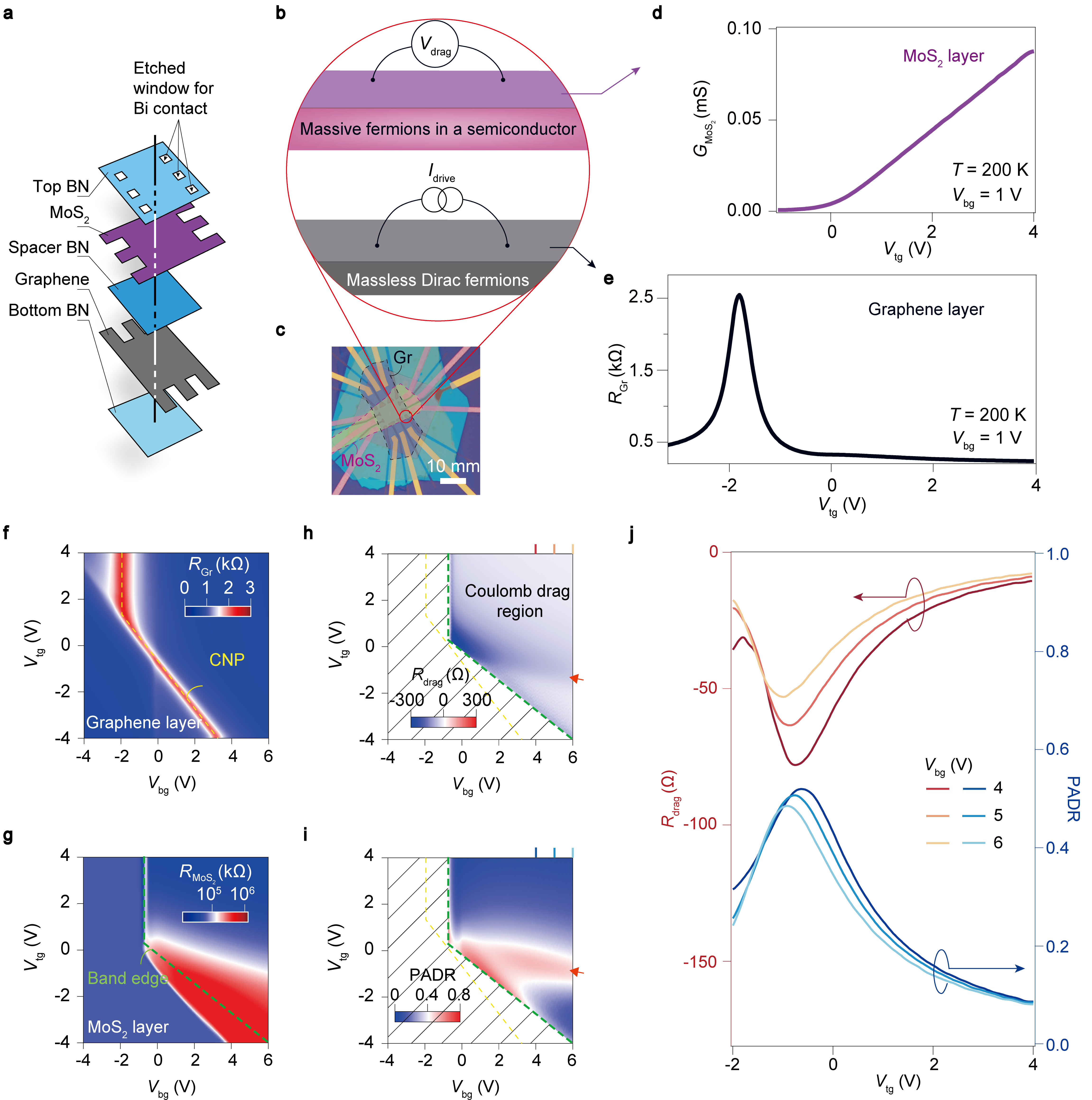
Monolayered graphene, few-layered MoS2 and h-BN flakes were mechanically exfoliated from bulk crystals. The MoS2 layer is always placed as the upper layer in the drag devices in this study. As illustrated in Fig. 1a, the van der Waals heterostructure is stacked using the dry transfer method [30], and then encapsulated by top and bottom h-BN flakes, with the top h-BN etched into micron-metre sized 2D windows. A windowed contact method is thus deployed to achieve Ohmic contacts to the MoS2 channel throughout the temperature range from 5 to 300 K[31]. The device were equipped with dual metallic gates and electrodes of Ti/Au via standard lithography and electron-beam evaporation (fabrication details are available in Methods). More detailed fabrication processes can be seen in Supplementary Figures 1-3. We found that different bottom gate geometry will affect the Coulomb drag measurements (Supplementary Figure 4), and the main text will focus on the geometric configuration as illustrated in Supplementary Figure 1.
Figure 1b describes the essential nanostructure in this study – a semiconductor-semimetal drag hybrid, realized in a MoS2–graphene double layer separated by an ultrathin 3 nm h-BN dielectric. Here, considering the low energy physics at the Fermi level within the solid state gate doping range, charge carriers in MoS2 and graphene are massive Schrödinger and massless Dirac fermions, respectively. Figure 1c shows the optical micrograph of a typical drag device (Sample S21, in which a bilayer MoS2 is utilized), with the corresponding fabrication flow shown in Supplementary Figure 3. Within the device, carriers in each layer can be tuned independently. For instance, at = 200 K, typical field effect curves in the graphene channel (Fig. 1d) and in the MoS2 channel (Fig. 1e) can be well obtained, respectively.
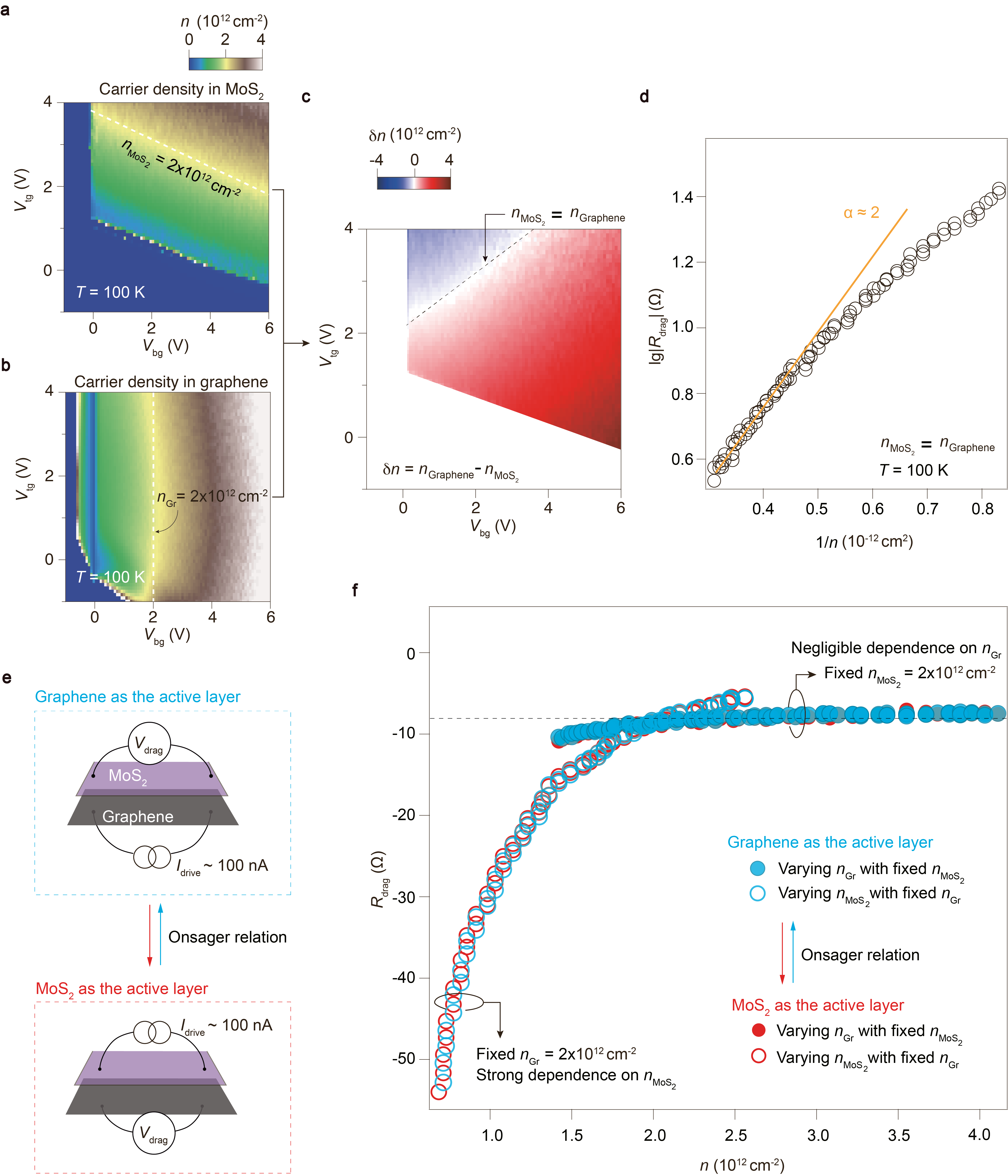
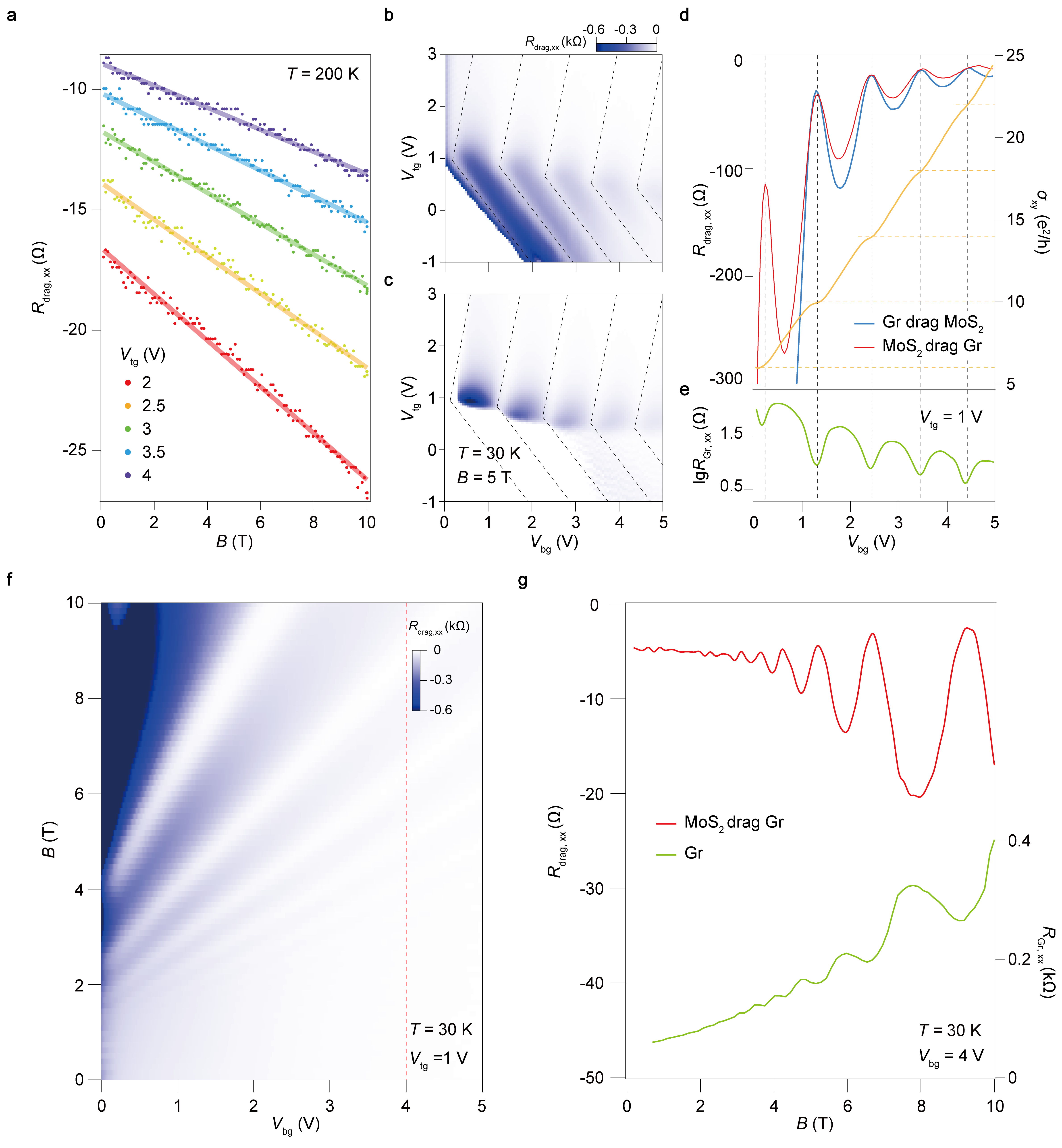
Figure 1f-g illustrate the mapping of longitudinal channel resistance and (in a log scale for visual clarity) in the same - space at = 200 K in the drag device Sample S21. In general, as shown in Fig. 1f, is in agreement with the previous observation in a standard dual-gated monolayer graphene devices [32]. However, the charge neutral resistive peak of graphene is partially screened by MoS2 due to the existence of relatively high carrier density in the latter layer, yielding a weak dependence of at larger than 1 V. Meanwhile, the band edge of MoS2 in Fig. 1g is squeezed and held almost constant at positive , which is likely due to the contact part of the MoS2 is not gated by the same gate as its major channel. Notice that the band edge of semiconducting MoS2 in Fig. 1g is highlighted by green dashed line, which is quantitatively extracted from the phase signal in the lock-in measurement, shown in Supplementary Figure 5.
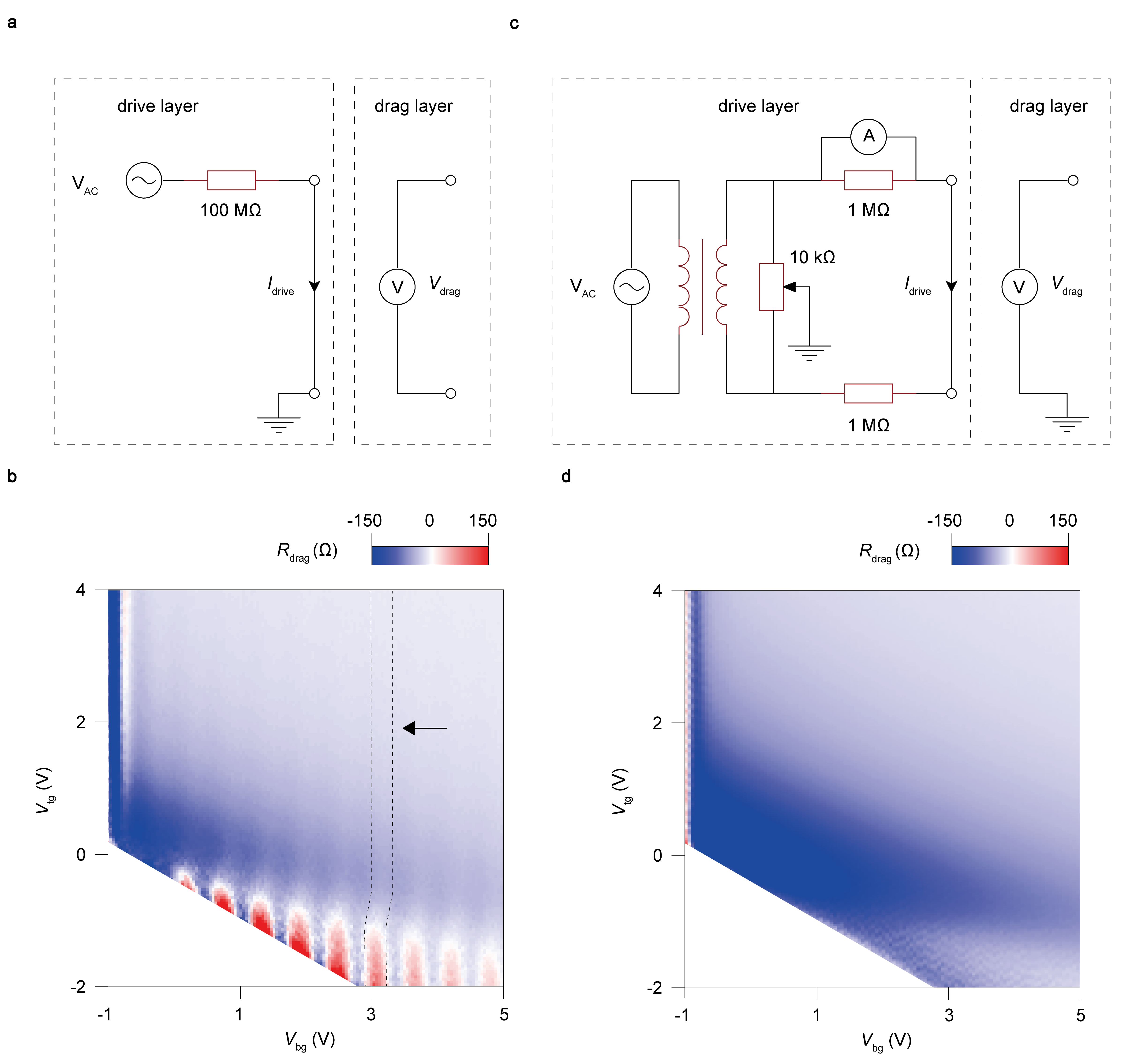
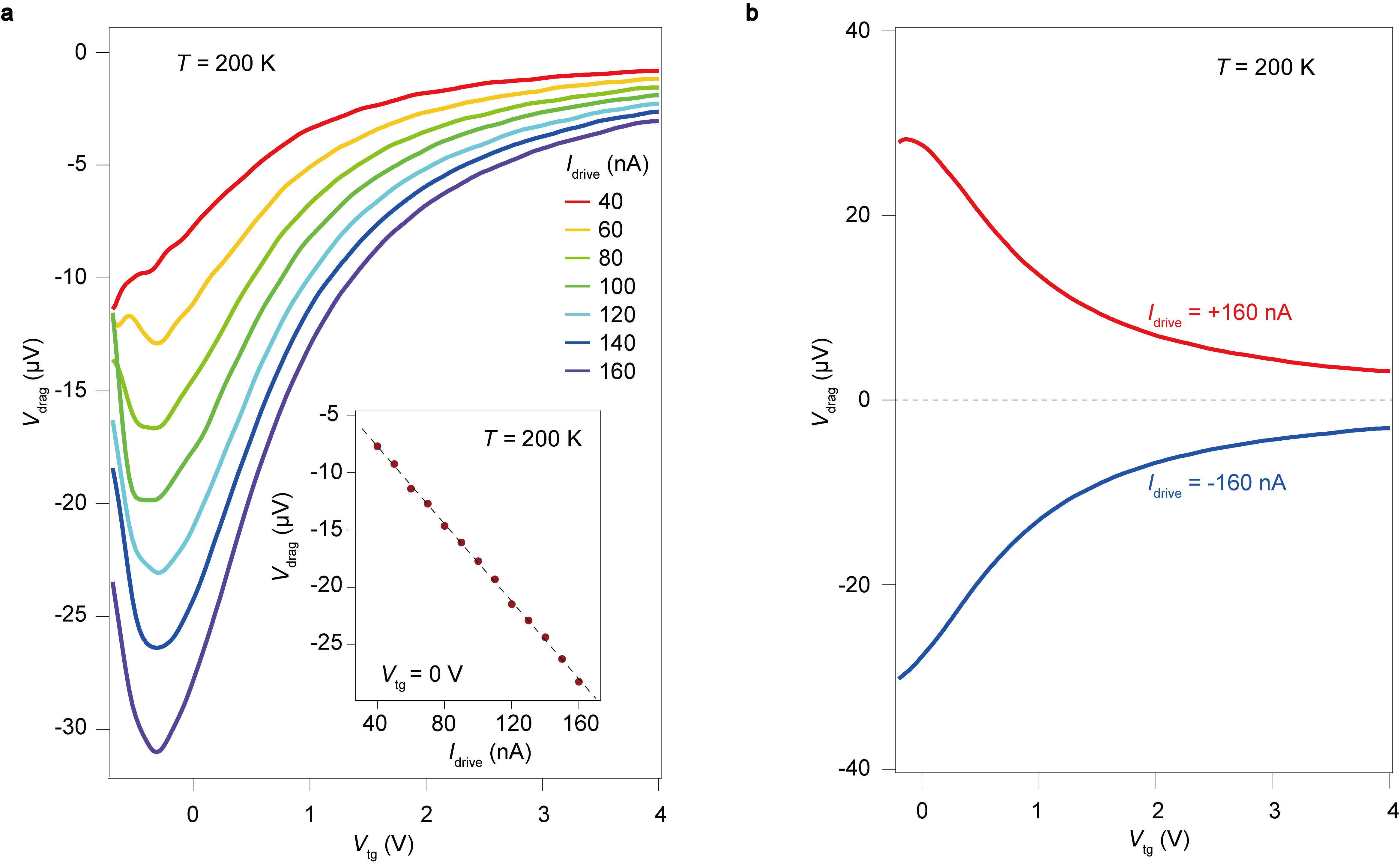
As a consequence, limited by the screening effect and the contact barriers, drag response in the current device is confined to the electron-electron regime, making hole drag not accessible. For the drag measurements, we passed a drive current () through the active layer and measured the resulting voltage drop () across the passive layer under open-circuit conditions. To eliminate spurious drag signals in the passive layer caused by drive-bias-induced AC gating effects[33], we have adopted a balance-bridge setup (comparison between lock-in measurement and the bridge methods can be seen Extended Data Figure 1)[10]. The linear relationship between and confirms the validity of our drag measurements, with the drag resistance determined by the slope of the curve (Extended Data Figure 2). Figure 1h shows the drag resistance using graphene as the driving layer (, the active layer). Here, the parasitic signals, determined to be coincides with the band edge of MoS2 by the phase measurements in Supplementary Figures 5-6, are blanked for visual clarity. The results of drag responses are reproducible in different samples, as shown in Supplementary Figure 7. The PADR, defined as , is usually a direct measure of the interlayer interaction in drag systems. For example, when it comes to a perfect drag in the scenario of exciton condensation, PADR may reach the unity[34, 12, 35]. In our system, PADR (Fig. 1i) has a maximum value of 0.6 when MoS2 serves as the active layer, much higher compared to most of the conventional drag systems. Moreover, we notice that maximum seems to take place at the onset of the semiconducting MoS2 channel conductance derivative with respect to gate voltage (), as indicated by the red arrows in Fig. 1h-i (aslo discussed in Supplementary Figure 8). Line profiles of and PADR as a function of at typical are shown in Fig. 1j. The maximum value of PADR increases as the gate voltage decreases form 6 to 4 V.
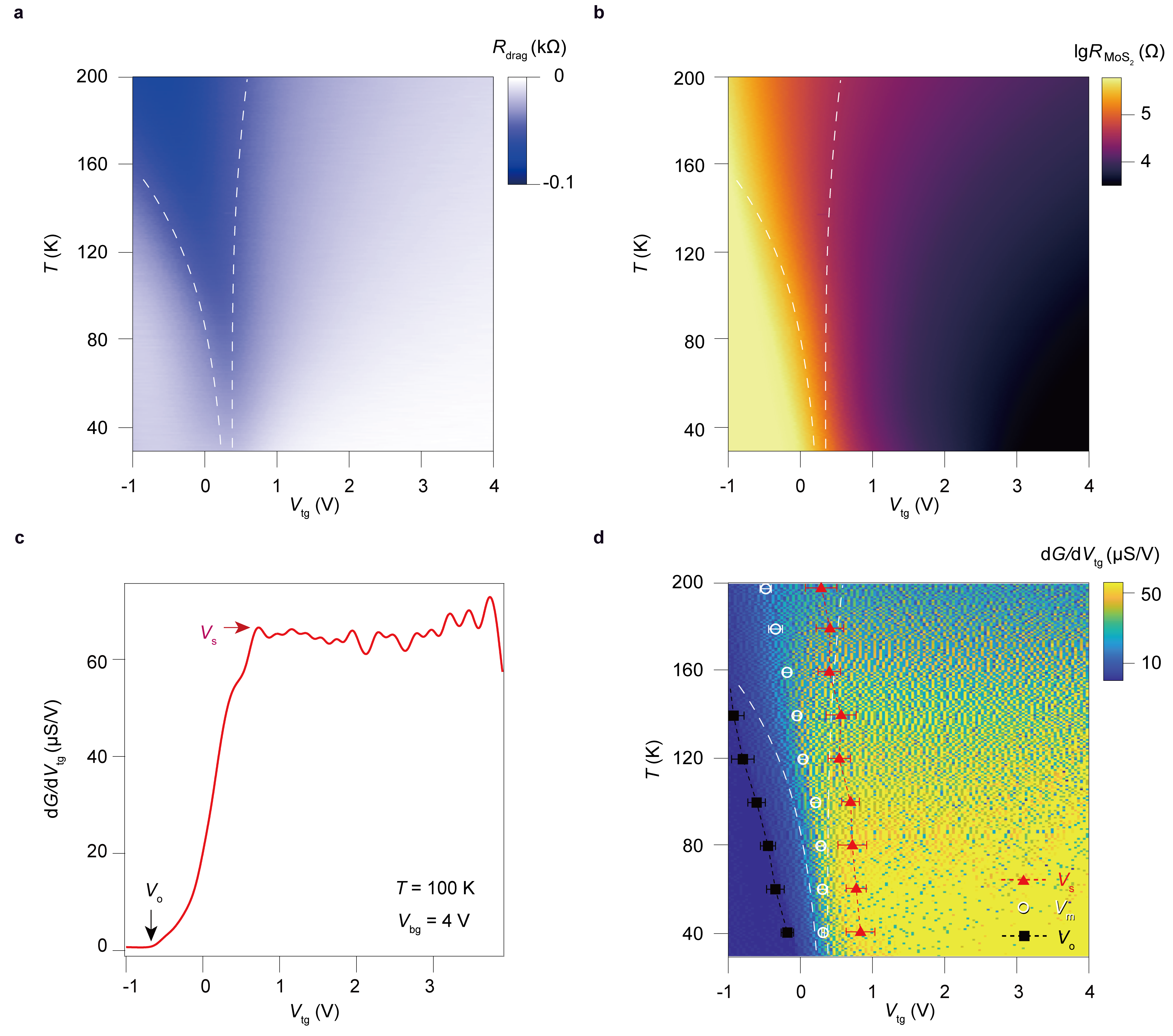
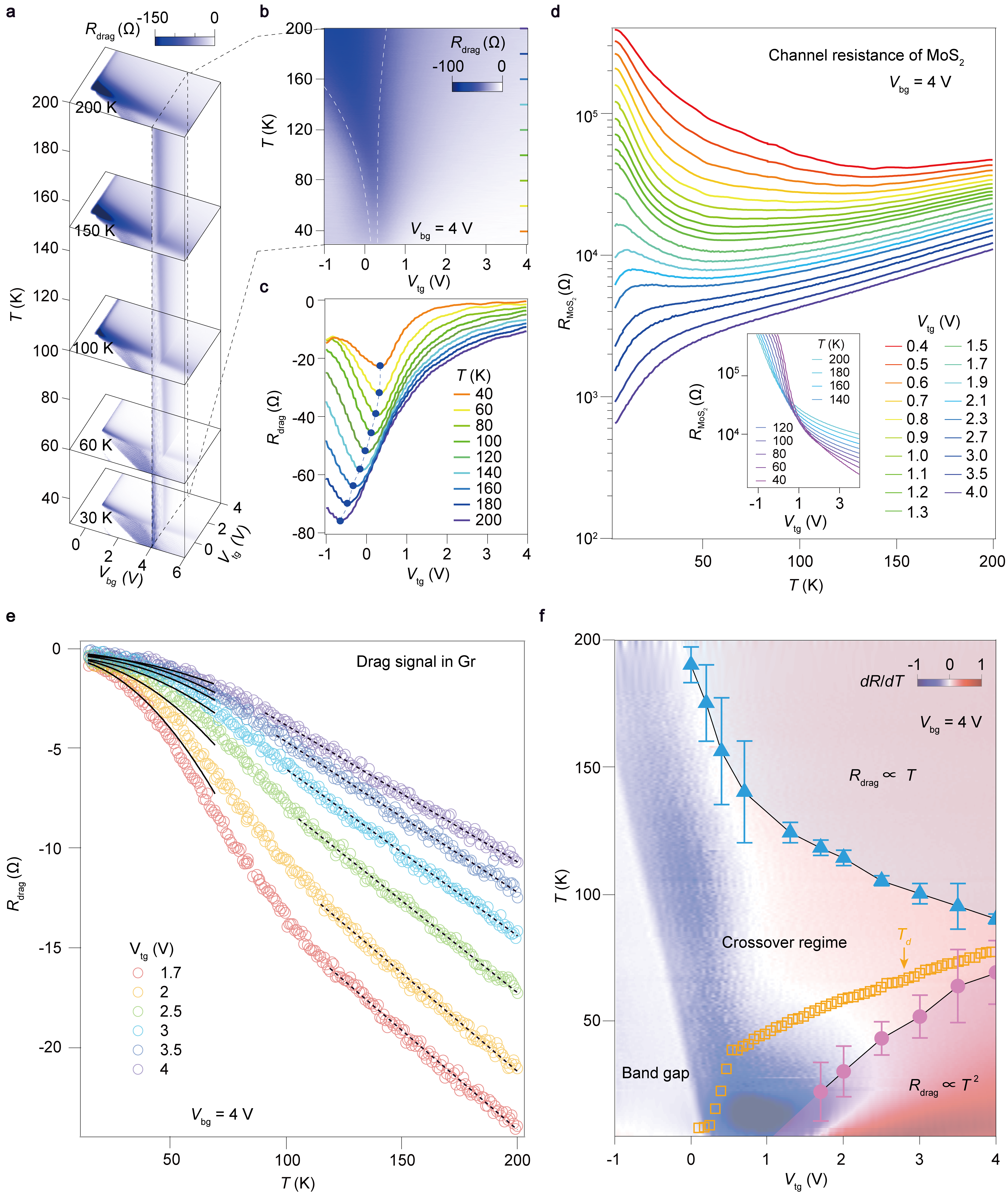
Temperature dependences of the Coulomb drag in the semiconductor-semimetal hybrid. In the following, we investigate the observed drag response in the graphene-MoS2 hybrid at different temperatures. Figure 2a overlays with MoS2 being the active layer in the - space at = 200, 150, 100, 60 and 30 K, respectively. It is seen that the maximum line (alongside the onset of for the MoS2 channel, as seen in Extended Data Figure 3) is shifted slightly toward higher upon lowering the temperature. Indeed, this feature is better captured in the mapping as a function of and , as shown in the vertical mapping in Fig. 2a (with MoS2 being the active layer) and Fig. 2b (with graphene being the active layer). The line cuts along the colored ticks (which correspond to different temperatures) in Fig. 2b are shown in Fig. 2c. It is clear that a maximum negative is identified in each curve, highlighted by blue solid dots. Discussions on the agreement between the maximum and of the MoS2 channel can be seen in Extended Data Figure 3.
Interestingly, when lowering the temperature, phonon scattering in the MoS2 is known to be largely suppressed and the carrier transport in the system is supposed to be driven from phonon-limited low mobility regime into the intrinsic high mobility regime, with the system exhibiting a transition from insulating behavior to a metallic one, known as metal-insulator transition (MIT) when varying from low to high carrier density in the low temperature limit[36, 37, 31]. Indeed, in Sample S21, clear MIT in the MoS2 channel can be seen in Fig. 2d, with its inset displaying the channel resistance of MoS2 at different temperatures. The linear - curves of the MoS2 channel at different temperatures are plotted in Supplementary Figure 9. This highly tunable electron transport properties in one of the layers of the drag system may give rise to unique and unconventional drag signals, distinguishing it from previously reported drag systems[38, 39, 40, 21]. Fig. 2e shows the temperature dependence of drag resistance at different with the fixed at 4 V. increases monotonically as the temperature increases when MoS2 becomes metallic at large . A dependence is clearly observed at the base temperatures, which is in good agreement with the theory of frictional drag for Fermi liquid[41, 42]. However, in the high-temperature regime, deviation from the dependence becomes pronounced, eventually evolving into a linear temperature dependence. It is found that the crossover regime from to dependence broadens as MoS2 becomes more insulating with decreasing .
In order to further analyze the correlation between the drag and pristine transport property of MoS2, we compare the color maps of the temperature-dependent resistance deviation () of MoS2 with the drag resistance in the - phase diagram (Fig. 2f). The corresponding fitting points for in Fig. 2e are featured in the phase diagram. From this comparison, we identify four distinct temperature-dependent drag regions. The white region in the color map of marks the boundary between the metallic and insulating phases of MoS2. On the metallic side of MoS2, with the line profiles of the drag resistance already presented in Fig. 2e, clear , and - crossover regions are observed. Coulomb drag resistance is known to be extremely sensitive to temperature, interlayer spacing, carrier density (or density mismatch between the layers) and magnetic field[22, 43]. And drag transport regimes can be defined by the Fermi energy , Fermi momentum , interlayer separation . In the Boltzmann-Langevin theory of Coulomb drag, at low temperatures () and in the clean limit (weak disorder or low scattering rate), drag is dominated by the particle-hole continuum and is proportional to [44]. Thus, we have plotted the estimated characteristic temperature in the phase diagram and found that the curve of indeed separates the quadratic and linear dependent drag regimes. The temperature region of a Fermi liquid below , in which the drag resistance follows the law, is strongly suppressed as the MIT boundary is approached. At higher temperatures, , phase-space constraints due to small-angle scattering lead to a linear temperature dependence[44, 2]. While on the insulating side, deviates from both and linear temperature dependence, eventually drops to zero as the carrier density in MoS2 decreases and Fermi level moves into the bandgap of MoS2.
| Drag category | Drag system | dependence | dependence | dependence | Maximum drag resistance | Ref. |
| Massless-massless fermions | ML Gr-ML Gr | (high density) | N/A | anomalous | 50 | [3] |
| ML Gr-ML Gr | (0 T) | N/A | 400 (70 K, 1 T at CNP) | [48] | ||
| Massless-massive fermions | ML Gr-CNT | (when ) | N/A | 6 (260 K) | [15] | |
| ML Gr-InAs NW | 0.5 (1.5 K) | [18] | ||||
| ML Gr-GaAs 2DEG | N/A | N/A | 2 (0.24 K) | [27] | ||
| ML Gr-BL | (high density) | (low density), (high density) | N/A | 5 (high density), 50 (CNP) | [47] | |
| ML Gr-BL | 0.3 k (200 K, 0 T) | This work | ||||
| Massive-massive fermions | BL Gr-BL Gr | decreases as increases | N/A | N/A | 800 (1.5 K at CNP) | [21] |
| BL Gr-BL Gr | (nonlocal), (local) | (nonlocal, low density) | N/A | 60 (CNP) | [22] | |
| ML -ML | (<10 K) | N/A | 1 M (1.5 K) | [34] | ||
| FL -FL | N/A | N/A | 2.5 M (1.5 K) | [38] | ||
| BL Gr-GaAs 2DEG | N/A | (high density) | N/A | 2 (70 K) | [46] | |
| Others | ML Gr-LAO/STO | 0.2 K | N/A | N/A | 0.5 (0.2 K) | [13] |
| InAs-GaSb topological wires | decreases as increases | N/A | N/A | 0.8 k (0.3 K) | [14] | |
| ML Gr-Gr/BN moiré superlattice | (high density) | (high density) | N/A | 10 (CNP) | [39] |
Drag at the matched density. It is noticed that the carrier density dependent characteristic of varies significantly in different kinds of drag system. The relationship between drag resistance and carrier density at the matched density ( = ) in massive-massless fermion system has been explored theoretically, which is in contrast with that in massive-massive and massless-massless fermion systems[45, 25]. For high density regime (), all three systems exhibit a similar carrier density dependence, specifically following an behavior. For the low density regime (), the carrier density dependence exhibits distinct characteristics for different systems, highlighting their unique properties. Specifically, in the massless-massive case, scales as , whereas for massive-massive and massless-massless systems, the dependencies are predicted to follow and , respectively[42, 25]. In our case, we first estimate and independently from the longitudinal and transverse resistance ( and , respectively) of the MoS2 and graphene layers based on measurements of the classical Hall effect at 100 K, as shown in Fig. 3a and b. The of both MoS2 and graphene varies linearly with the magnetic field, as shown in Supplementary Figure 10. The equal density line ( = ) can be easily identified by subtracting the two carrier density color maps of MoS2 and graphene, as illustrated by the black dash line in Fig. 3c. Subsequently, we plot the drag resistance along the density matched line ( = ) in logarithmic scale and converges to the expected dependence, with . For our massive-massless fermion system, the range of the equal density line is about . Thus, we estimate that the maximum value of satisfies using the expression . This result demonstrates the equal density line is at the low density regime with the dependent , which agrees well with the theoretical predicts[25].
In addition to the matched density condition, we also explore the density-dependent drag resistance in the non-equal density case () to examine the varying capabilities of controlling the drag signal by the two different layers. In the following analysis, we selectively sweep the top and bottom gate voltages, in order to adjust the carrier density of MoS2 (or graphene) independently while keeping the density of graphene (or MoS2) constant, and consider the Onsager reciprocal relations (illustrated schematically in the measurement configuration of Fig. 3e) of the resulted drag responses. We use the same density of MoS2 or graphene, fixed at (indicated by the white dashed lines in Fig. 3a-b for and , respectively) for comparison. Noticeably, the drag resistance exhibits a pronounced dependence on , while showing a weak dependence on . The validity of the Onsager reciprocal relations is confirmed for the decoupled density-dependent drag results, as evidenced by the agreement between the blue and red symbols, where the active layer is graphene and MoS2, respectively. In both cases, variations in only are indicated by solid circles, while variations in only are indicated by open circles. Note that the results in Fig. 3f are not consistent with the drag response reported for the MLG-BLG massive-massless fermion system, where the drag resistance follows the functional dependence or the conventional , where and are the carrier densities of top and bottom layers[46, 47, 1]. Our results demonstrate that, in 2D semicondutor-graphene drag system, the control ability of over the drag signal may be one order of magnitude smaller than that of , and applies under certain conditions. It may be originated from the much stronger electron correlations in the semiconductor MoS2 compared to the semimetallic graphene.
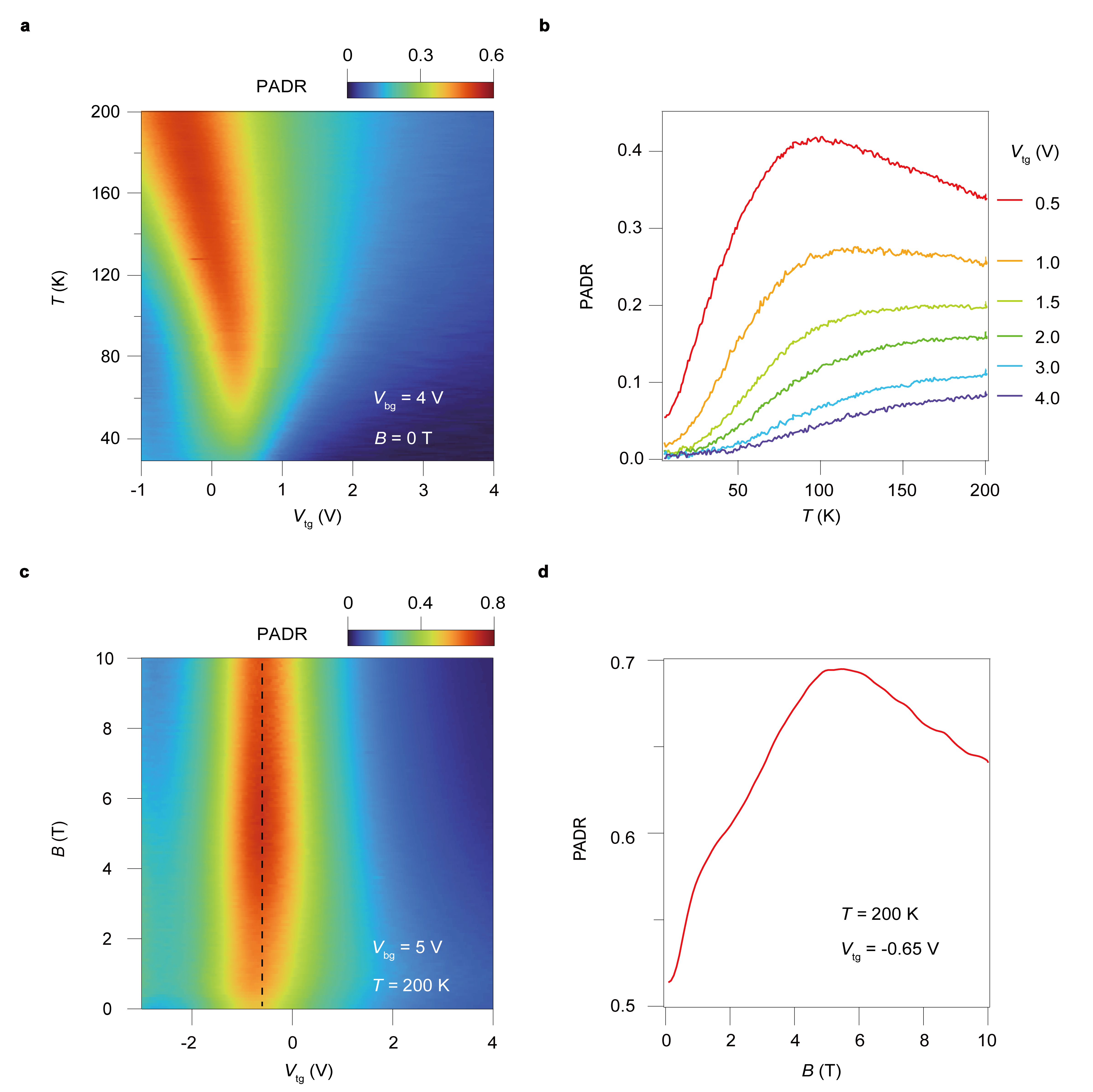
Magneto-drag in the MoS2-graphene hybrid. Finally, we show the magnetodrag (the longitudinal component) of massive-massless fermion system in the presence of a finite magnetic field . We first investigate the -dependent at 200 K, when graphene and MoS2 are not in the quantum hall regime as shown in Fig. 4a. Remarkably, does not exhibit the conventional frictional drag dependence but instead shows a linear behavior at different top gate voltages from = 2 to 4 V, accompanied by the linear -dependence observed at high temperatures (Fig. 2e-f). When the temperature is further lowered to 30 K, the graphene layer enters the quantum Hall state with integer Landau level (LL) filling fractions at 5 T (see Supplementary Figure 11), whereas MoS2 doesn’t. Consequently, magnetodrag in both Fig. 4b and 4c show well-developed stripped features (highlighed by the broken lines), which are regions of nearly zero drag responses. The reciprocal magnetodrag along with the longitudinal resistance and transverse conductance of graphene at 30 K and 5 T are clearly shown in Fig. 4d and 4e, respectively. The Onsager reciprocity is still valid and the observed minimum absolute values of oscillations in magnetodrag signal are consistent with the gapped states between LLs in graphene. Therefore, the vanishing drag signals arise from inefficient drag due to the insulating and incompressible nature of the graphene bulk, which leads to a vanishing density of states for interlayer Coulomb scattering[49, 48]. This phenomenon becomes more pronounced when the magnetic field becomes larger (see Supplementary Figures 12-13). It is noteworthy that Onsager reciprocal relation is only valid when MoS2 becomes metallic. Fig. 4f shows the fan diagram of magnetodrag as a function of at 30 K, with as the active layer. The fan diagram of magnetodrag is similar to that obtained in the pristine graphene channel and held valid for the Onsager reciprocity relation, as shown in Supplementary Figure 14. The absolute magnitude of the drag signal increases with the magnetic field and the smallest measured magnitudes of oscillations in the magnetodrag signal align with the presence of gaps between Landau levels in graphene, as displayed in Fig. 4g. Shown in Table 1, characteristics of temperature, magnetic field, and carrier density dependence in a collection of experimentally tested Coulomb drag systems[21, 3, 48, 15, 18, 27, 47, 34, 38, 22, 46, 13, 14, 39] are summarized. Compared to those reported, the massless Dirac -massive Schrödinger fermions graphene-MoS2 drag system in this work demonstrates an unconventional crossover from to -dependence (Fig. 2e-f), as well as a linear magneto-drag response (Fig. 4a), providing a distinct paradigm for future theoretical considerations.
To conclude, by introducing semiconducting TMD channel with Ohmic contacts, we have devised a drag system consisting of graphene–MoS2 heterostructure separated by an ultrathin h-BN dielectric. It demonstrates the emergence of a large Coulomb drag response, along with a transition from linear to quadratic temperature dependence of the drag resistance, accompanied by the metal-insulator transition in MoS2. The experimental platform enables precise control over intralayer interaction-driven drag by independently tuning carrier densities in each layer, offering new insights into the interplay between massive Schrödinger and massless Dirac carriers. The dominance of a large Wigner–Seitz radius (>10) in MoS2 indicates that electron correlations play a crucial role in shaping the drag response, with graphene acting as a passive layer. Furthermore, a linear magneto-drag response was observed in the graphene–MoS2 heterostructure drag devices, distinguishing it from previously known systems. Our findings enrich the drag family and suggest that a semiconductor-semimetal double-layer 2D electronic system may be intriguing for the design of unique interaction physics in Coulomb drag charge transports.
Methods
Sample fabrication. vdW few-layers of the h-BN//h-BN/graphene/h-BN sandwich were obtained by mechanically exfoliating high quality bulk crystals. The vertical assembly of vdW layered compounds were fabricated using the dry-transfer method in a nitrogen-filled glove box. The heterostructures were then transferred onto the pre-fabricated Au or graphite gates. Hall bars of the devices were achieved by reactive ion etching. During the fabrication processes, electron beam lithography was done using a Zeiss Sigma 300 SEM with a Raith Elphy Quantum graphic writer. One-dimensional edge contacts of monolayer graphene were achieved by using the electron beam evaporation with Ti/Au thicknesses of 5/50 nm and the window contacts of bilayer were fabricated with a thermal evaporator, with typical Bi/Au thicknesses of 25/30 nm. After atomic layer deposition of about 20 nm Al2O3, big top gate was deposited to form the complete dual gated h-BN encapsulated drag devices as shown in Fig. 1a and c.
Drag measurements. In lock-in measurements, current is typically driven by applying an AC bias voltage to one side of the channel while the other side is grounded. However, in Coulomb drag measurements, applying this bias to the drive layer may induce spurious drag signals in the drag layer due to the AC gating effect caused by the drive bias. Here we applied about 0.2 0.3 V AC bias voltage at 17.777 Hz to drive the active layer through a 1:1 voltage transformer. The transformer was connected to a 10 k potentiometer, which can help to distribute the AC voltage across both ends of the driving layer. This configuration minimizes the AC interlayer potential difference in the channel, thereby reducing the AC coupling between the active and passive layers. We used two 1 M resistors connected with the driving layer and measured the voltage drop across one of the resistors to obtain the driving current. The drag voltages were recorded using low-frequency SR830 lock-in amplifiers. Four-probe measurements were used throughout the transport measurements in an Oxford Teslatron cryostat. Gate voltages on the as-prepared devices were controlled by a Keithley 2400 source meter.
Data Availability
The data that support the findings of this study are available upon reasonable request to the corresponding authors.
Code Availability
The code that support the findings of this study are available upon reasonable request to the corresponding authors.
References
- [1] Narozhny, B. & Levchenko, A. Coulomb drag. Reviews of Modern Physics 88, 025003 (2016).
- [2] Jauho, A.-P. & Smith, H. Coulomb drag between parallel two-dimensional electron systems. Physical Review B 47, 4420 (1993).
- [3] Gorbachev, R. et al. Strong Coulomb drag and broken symmetry in double-layer graphene. Nature Physics 8, 896–901 (2012).
- [4] Kellogg, M., Eisenstein, J., Pfeiffer, L. & West, K. Bilayer quantum all systems at = 1: Coulomb drag and the transition from weak to strong interlayer coupling. Physical review letters 90, 246801 (2003).
- [5] Eisenstein, J. & MacDonald, A. H. Bose–einstein condensation of excitons in bilayer electron systems. Nature 432, 691–694 (2004).
- [6] Kellogg, M., Spielman, I., Eisenstein, J., Pfeiffer, L. & West, K. Observation of quantized all drag in a strongly correlated bilayer electron system. Physical review letters 88, 126804 (2002).
- [7] Kellogg, M., Eisenstein, J., Pfeiffer, L. & West, K. Vanishing all resistance at high magnetic field in a double-layer two-dimensional electron system. Physical review letters 93, 036801 (2004).
- [8] Tutuc, E., Shayegan, M. & Huse, D. Counterflow measurements in strongly correlated as hole bilayers: Evidence for electron-hole pairing. Physical review letters 93, 036802 (2004).
- [9] Nandi, D., Finck, A., Eisenstein, J., Pfeiffer, L. & West, K. Exciton condensation and perfect coulomb drag. Nature 488, 481–484 (2012).
- [10] Liu, X., Watanabe, K., Taniguchi, T., Halperin, B. I. & Kim, P. Quantum all drag of exciton condensate in graphene. Nature Physics 13, 746–750 (2017).
- [11] Liu, X. et al. Crossover between strongly coupled and weakly coupled exciton superfluids. Science 375, 205–209 (2022).
- [12] Li, J., Taniguchi, T., Watanabe, K., Hone, J. & Dean, C. Excitonic superfluid phase in double bilayer graphene. Nature Physics 13, 751–755 (2017).
- [13] Tao, R. et al. Josephson–coulomb drag effect between graphene and a superconductor. Nature Physics 19, 372–378 (2023).
- [14] Du, L. et al. Coulomb drag in topological wires separated by an air gap. Nature Electronics 4, 573–578 (2021).
- [15] Anderson, L., Cheng, A., Taniguchi, T., Watanabe, K. & Kim, P. Coulomb drag between a carbon nanotube and monolayer graphene. Physical Review Letters 127, 257701 (2021).
- [16] Laroche, D., Gervais, G., Lilly, M. & Reno, J. 1D-1D Coulomb drag signature of a Luttinger liquid. Science 343, 631–634 (2014).
- [17] Tabatabaei, S. M., Sánchez, D., Yeyati, A. L. & Sánchez, R. Andreev-Coulomb drag in coupled quantum dots. Physical Review Letters 125, 247701 (2020).
- [18] Mitra, R. et al. Anomalous coulomb drag between nanowire and graphene heterostructures. Physical Review Letters 124, 116803 (2020).
- [19] Das Sarma, S., Adam, S., Hwang, E. & Rossi, E. Electronic transport in two-dimensional graphene. Reviews of modern physics 83, 407–470 (2011).
- [20] Das Sarma, S., Hwang, E. & Tse, W.-K. Many-body interaction effects in doped and undoped graphene: Fermi liquid versus non-Fermi liquid. Physical Review B—Condensed Matter and Materials Physics 75, 121406 (2007).
- [21] Lee, K. et al. Giant frictional drag in double bilayer graphene heterostructures. Physical review letters 117, 046803 (2016).
- [22] Li, J. et al. Negative Coulomb drag in double bilayer graphene. Physical review letters 117, 046802 (2016).
- [23] Lin, J. et al. Determining interaction enhanced valley susceptibility in spin-valley-locked . Nano letters 19, 1736–1742 (2019).
- [24] Ahn, S. & Das Sarma, S. Density-tuned effective metal-insulator transitions in two-dimensional semiconductor layers: Anderson localization or Wigner crystallization. Physical Review B 107, 195435 (2023).
- [25] Scharf, B. & Matos-Abiague, A. Coulomb drag between massless and massive fermions. Physical Review B—Condensed Matter and Materials Physics 86, 115425 (2012).
- [26] Principi, A., Carrega, M., Asgari, R., Pellegrini, V. & Polini, M. Plasmons and Coulomb drag in Dirac-Schrödinger hybrid electron systems. Physical Review B—Condensed Matter and Materials Physics 86, 085421 (2012).
- [27] Gamucci, A. et al. Anomalous low-temperature Coulomb drag in graphene-GaAs heterostructures. Nature communications 5, 5824 (2014).
- [28] Duan, J.-M. & Yip, S. Supercurrent drag via the Coulomb interaction. Physical review letters 70, 3647 (1993).
- [29] Huang, X., Bazan, G. & Bernstein, G. H. Observation of supercurrent drag between normal metal and superconducting films. Physical review letters 74, 4051 (1995).
- [30] Wang, L. et al. One-dimensional electrical contact to a two-dimensional material. Science 342, 614–617 (2013).
- [31] Zhao, S. et al. Fractional quantum hall phases in high-mobility n-type molybdenum disulfide transistors. Nature Electronics (2024).
- [32] Sanchez-Yamagishi, J. D. et al. Quantum Hall Effect, screening, and layer-polarized insulating states in twisted bilayer graphene. Phys. Rev. Lett. 108, 076601 (2012).
- [33] Hill, N. et al. Frictional drag between parallel two-dimensional electron gases in a perpendicular magnetic field. Journal of Physics: Condensed Matter 8, L557 (1996).
- [34] Nguyen, P. X. et al. Perfect Coulomb drag in a dipolar excitonic insulator. arXiv preprint arXiv:2309.14940 (2023).
- [35] Zhang, N. J. et al. Excitons in the fractional quantum all effect. Nature 637, 327–332 (2025).
- [36] Radisavljevic, B. & Kis, A. Mobility engineering and a metal–insulator transition in monolayer . Nature materials 12, 815–820 (2013).
- [37] Moon, B. H. et al. Soft Coulomb gap and asymmetric scaling towards metal-insulator quantum criticality in multilayer . Nature communications 9, 2052 (2018).
- [38] Huang, M., Wu, Z., Wang, N. & Chui, S.-T. Quantum solid phase and Coulomb drag in 2D electron–electron bilayers of . Advanced Electronic Materials 9, 2201105 (2023).
- [39] Wang, Y. et al. Coulomb drag in graphene/h-BN/graphene moiré heterostructures. Physical Review Letters 133, 186301 (2024).
- [40] Pillarisetty, R. et al. Coulomb drag near the metal-insulator transition in two dimensions. Physical Review B—Condensed Matter and Materials Physics 71, 115307 (2005).
- [41] Flensberg, K., Hu, B. Y.-K., Jauho, A.-P. & Kinaret, J. M. Linear-response theory of Coulomb drag in coupled electron systems. Physical Review B 52, 14761 (1995).
- [42] Narozhny, B., Titov, M., Gornyi, I. & Ostrovsky, P. Coulomb drag in graphene: perturbation theory. Physical Review B—Condensed Matter and Materials Physics 85, 195421 (2012).
- [43] Zhu, L. et al. Signature of quantum interference effect in inter-layer Coulomb drag in graphene-based electronic double-layer systems. Nature Communications 14, 1465 (2023).
- [44] Chen, W., Andreev, A. & Levchenko, A. Boltzmann-Langevin theory of Coulomb drag. Physical Review B 91, 245405 (2015).
- [45] Hwang, E., Sensarma, R. & Das Sarma, S. Coulomb drag in monolayer and bilayer graphene. Physical Review B—Condensed Matter and Materials Physics 84, 245441 (2011).
- [46] Simonet, P. et al. Anomalous Coulomb drag between bilayer graphene and a GaAs electron gas. New Journal of Physics 19, 103042 (2017).
- [47] Zhu, L. et al. Frictional drag effect between massless and massive fermions in single-layer/bilayer graphene heterostructures. Nano Letters 20, 1396–1402 (2020).
- [48] Liu, X. et al. Frictional magneto-Coulomb drag in graphene double-layer heterostructures. Physical Review Letters 119, 056802 (2017).
- [49] Tse, W.-K., Hu, B. Y.-K., Hong, J. & MacDonald, A. Magneto-Coulomb drag and Hall drag in double-layer Dirac systems. Physical Review Letters 122, 186602 (2019).
Acknowledgements
This work is supported by theNational Key RD Program of China (Grant Nos. 2024YFA1410400, and 2022YFA1203903) and the National Natural Science Foundation of China (NSFC) (Grant Nos. 12450003, and 92265203). Z.H. acknowledges the support of the Fund for Shanxi “1331 Project” Key Subjects Construction, and supports from the Innovation Program for Quantum Science and Technology (Grant No. 2021ZD0302003). K.W. and T.T. acknowledge support from the JSPS KAKENHI (Grant Numbers 20H00354 and 23H02052) and World Premier International Research Center Initiative (WPI), MEXT, Japan.
Author Contributions
S.Z., Z.H., and W.R. conceived the experiment and supervised the overall project. Y.L. and S.Z. performed the device fabrications and electrical measurements; K.Y. contributed to electrical measurements; K.W. and T.T. provided high quality h-BN bulk crystals; S.Z., Y.L. and Z.H. analysed the experimental data. The manuscript was written by Z.H., S.Z. and Y.L. with discussions and inputs from all authors.
Competing Interests
The authors declare no competing interests.