Performance and radiation damage mitigation strategy for silicon photomultipliers on LEO space missions
Abstract
Space missions require lightweight, low-power consuming, radiation-tolerant components. Silicon photomultipliers are increasingly used for detecting near-UV, optical, and infrared light in space due to their compact design, low cost, low power consumption, robustness, and high photo-detection efficiency, which makes them sensitive to single photons. Although SiPMs outperform traditional photomultiplier tubes in many areas, concerns about their radiation tolerance and noise remain. In this study, we estimate the radiation effects on a satellite in sun-synchronous low Earth orbit (LEO) at an altitude of 550 km during the declining phase of solar cycle 25 (2026–2029). We evaluated silicon photomultipliers produced by the Foundation Bruno Kessler (FBK) using front-side illuminated technology with metal trenches (NUV-HD-MT), assessing their response to a 50 MeV proton beam and exposure to a -radioactive source (strontium-90). Simulations with SPENVIS and Geant4 were used to validate the experimental results. Based on our findings, we propose a photosensor annealing strategy for space-based instruments.
1 Introduction: silicon photosensors in space applications
Silicon photomultipliers (SiPMs) offer high photon detection efficiency (PDE) and low-power consumption, making them ideal candidates for a range of space applications [1, 2, 3, 4]. One of the key advantages of SiPMs is their ability to operate efficiently in low-light conditions. Their compact size and robustness also make them well-suited for integration into lightweight space instruments.
However, a major downside when using SiPMs in space missions is their susceptibility to radiation, which induces damages and degrades their performance over time. In addition, SiPMs are sensitive to temperature variations, requiring meticulous thermal management to ensure reliable operation in a harsh space environment. The work presented here aims to address these limitations in order to enhance the reliability and performance of SiPMs for space applications.
The NUSES [5] project will employ SiPMs for both of its payloads, Terzina [6] and Ziré [7]. Ziré, dedicated to monitoring of low-energy ( MeV) cosmic ray fluxes in the Van Allen belts, gamma-ray bursts in the energy region 1-10 MeV, space weather and lithosphere-ionosphere- magnetosphere couplings, will employ SiPMs with LYSO/GAGG crystals in the calorimeter (CALOg), in the plastic scintillator tower (PST) reading scintillating tiles, and in the FTK fiber tracker.
In this work, we consider the effects of radiation for the Terzina camera [8]. Differently than the Ziré detectors, the camera will be more exposed to the direct effect of radiation as it is not screened by scintillating material. Here, we present the results of a full characterisation of the sensors of the Fondazione Bruno Kessler (FBK) and an analysis of their response after irradiation to select a suitable sensor for the Terzina telescope [8].
Several other space missions are leveraging SiPM technology to advance our understanding of high-energy astrophysical phenomena. SiPMs are foreseen to be used for the HERD (High Energy Cosmic Radiation Detection) plastic scintillator detector [9]. HERD is a planned space-based experiment to study dark matter from space through the measurement of energy spectra and anisotropy of high energy electrons, as gamma-ray monitoring between 0.5 GeV and 100 TeV and to measure cosmic ray fluxes to the knee. A future mission following the paths of Ziré employing scintillating crystals read by SiPMs is Crystal Eye [10].
SiPMs play a crucial role in Cherenkov light detection in Terzina. The proposed POEMMA (Probe Of Extreme Multi-Messenger Astrophysics) mission [11, 12] firstly proposed to complement measurements of fluorescence with MAPMTs with Cherenkov detection with the more sensitive SiPMs. Cherenkov light is emitted by ultra-high-energy cosmic rays (UHECRs) and can also be detected from earth skimming astrophysical neutrinos when they produce extensive air showers (EAS) in the Earth’s atmosphere. This mission is preceded by several balloon flights under the JEM-EUSO (Joint Experiment Missions for Extreme Universe Space Observations) program [13, 14]. In particular, EUSO-SPB2 (Super Pressure Balloon-borned Telescope) [15, 16], launched in May 2023 from NASA’s Wanaka base in New Zealand [17], employed SiPMs for cosmic-ray detection from the stratosphere.
This study for Terzina, where the photosensor plane is directly exposed to cosmic radiation, is imperative. A previous study was performed by POLAR-2 [18], where SiPMs are coupled with scintillators as for other experiments. They amplify weak signals and provide protection against radiation damage, along with the shielding provided by the satellite structure. The POLAR-2 mission plans to use SiPMs for advanced gamma-ray burst (GRB) polarization studies and radiation hardness studies. Specifically regarding radiation hardness, they have proposed mitigation strategies that align with the work described here [19, 18].
The paper is structured as follows: in section 2, the Terzina telescope and its Focal Plane Assembly (FPA) are described. In section 3, we detail the results of the single SiPM characterisation that will compose the tiles of the FPA. In section 4, we describe the calculation of the fluxes of cosmic rays at the altitude of the NUSES orbit with the SPENVIS software [20]. In section 5, we estimated the ionizing and non-ionizing doses affecting the FPA through a Geant4-based [21, 22] simulation of the detector. In sections 6 and 7, a proton irradiation campaign of the SiPMs that will be used in the Terzina telescope is described together with the thermal response of the sensors. Moreover, the effect of the dose released by electrons has been taken into account (section 8). Finally, a discussion of the results and of a possible mitigation strategy for radiation damage are provided in section 9.
2 The Terzina telescope onboard NUSES
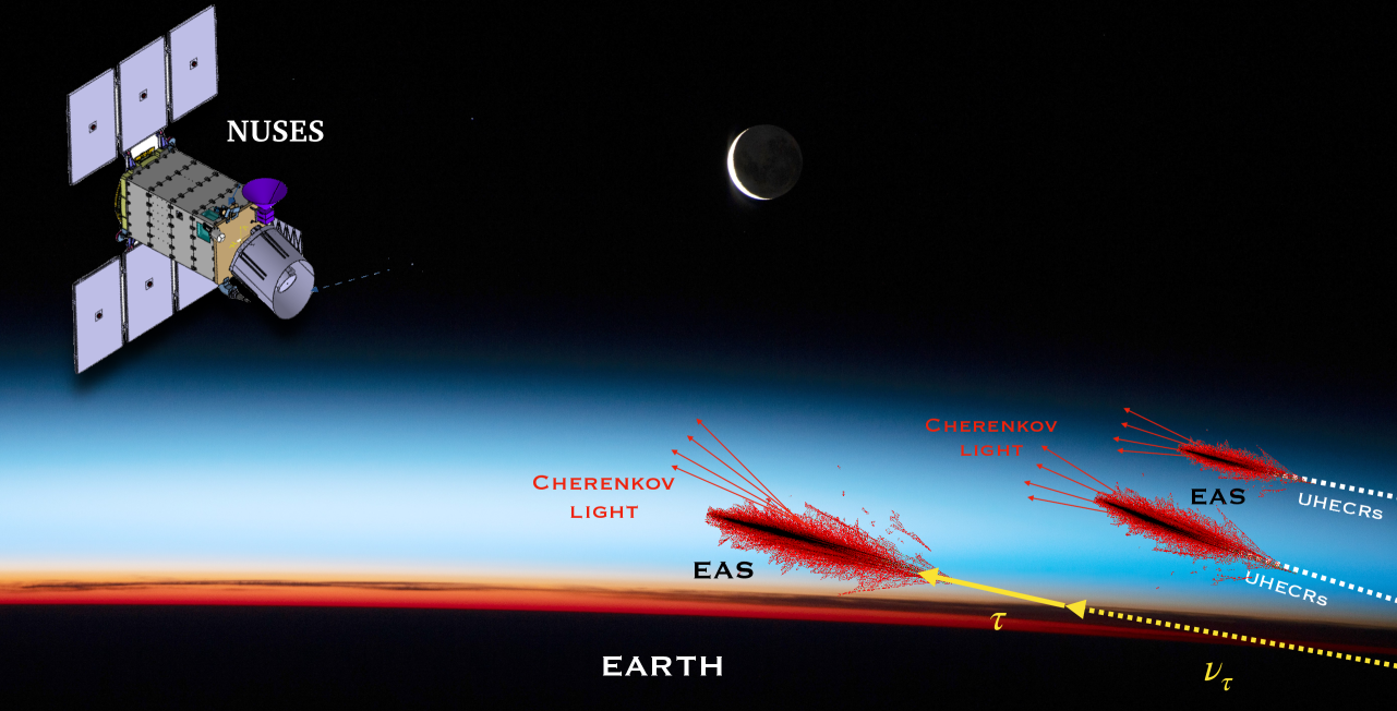
The NUSES ballistic mission aims to explore new scientific and technological pathways for future space-based astroparticle physics detectors. The satellite platform, developed by the industrial partner TAS-I (THALES Alenia Space - Italia), will operate in a quasi-polar Low Earth Orbit (LEO) at an altitude of 535 in the worst case and 550 km at the Beginning of Life (BoL). The satellite will host two instruments: Terzina and Ziré. It will follow a sun-synchronous orbit and operate in a dusk-dawn mode along the day/night boundary so that the Terzina telescope can point to the dark side of the Earth’s limb to detect the faint Cherenkov light from ultra-relativistic particle showers in the dark atmosphere. Terzina telescope aims at the first detection of this Cherenkov light, which can be detected within the field of view (FoV) of its camera located in the FPA. The FPA is designed to detect the Cherenkov light emitted by UHECR-induced EAS with energies above PeV and with their axis pointing upwards close to the optical axis of the telescope pointing to the limb.
The Earth’s limb is at the angle , where when km at BoL. while at the end of life, when the drag of the residual atmosphere will reduce the orbit altitude to 535 km. In addition, Terzina can detect the upward EAS produced in the atmosphere by the decay of tau and muon leptons generated by the respective neutrinos with energies above PeV, passing through the Earth. A pictorial view of the detection principle of the Terzina payload on the NUSES satellite is presented in figure 1, highlighting the instrument’s positions and pointing directions, though not in scale. Terzina is a pathfinder for future larger missions, such as POEMMA or a constellations of satellites as conceived for CHANT [23].
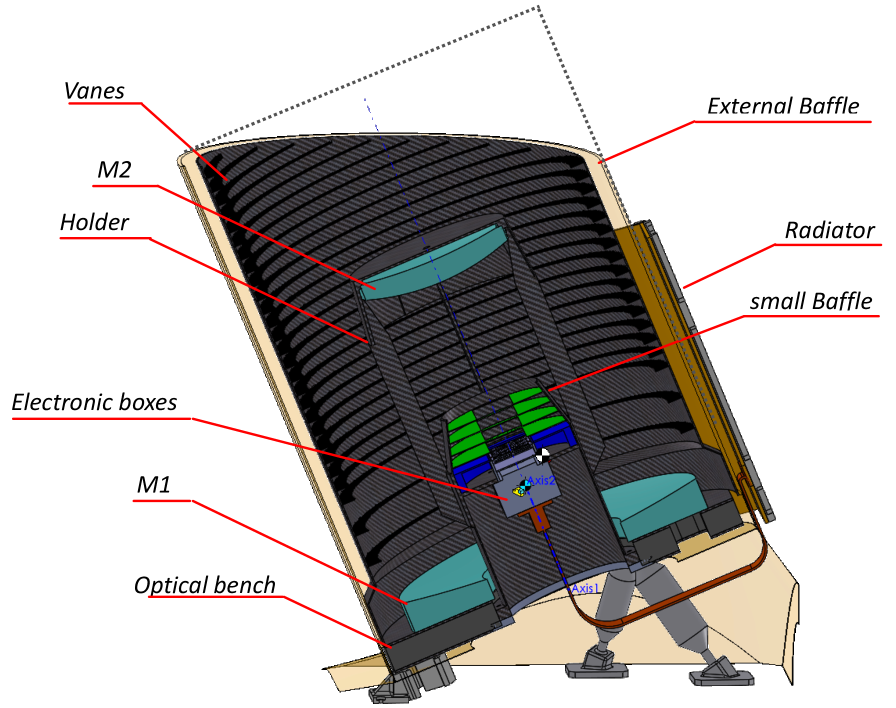
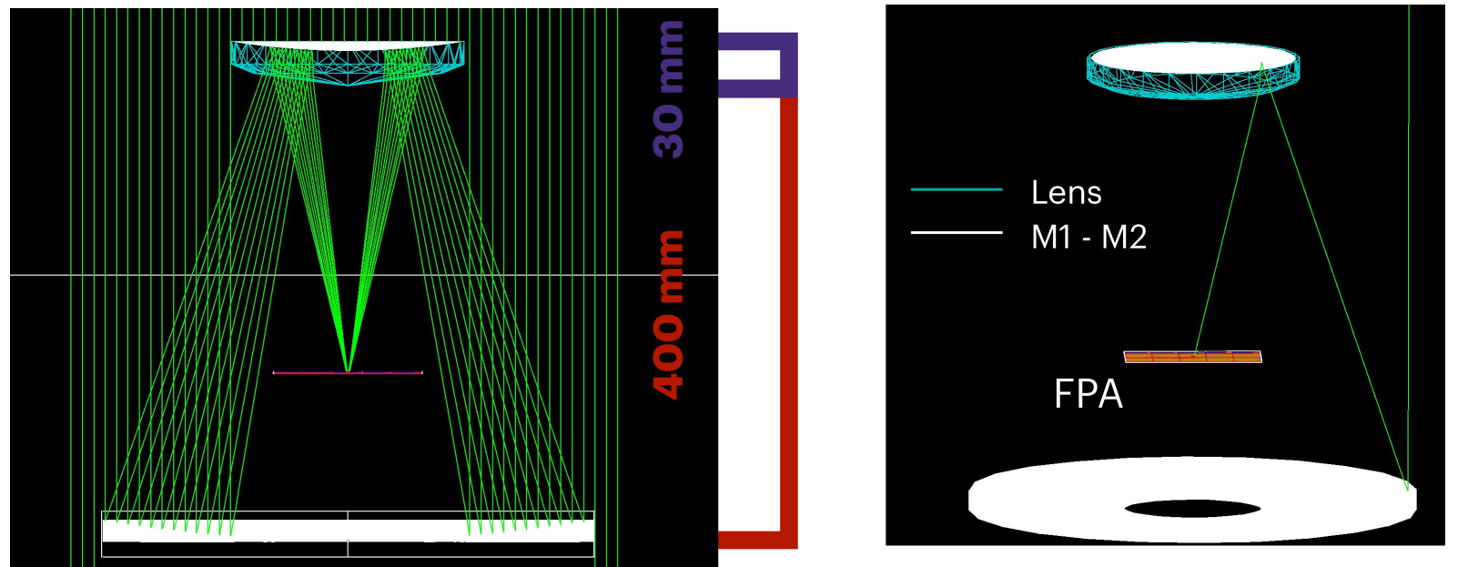
The Terzina detector consists of a near-UV optical telescope with Schmidt-Cassegrain optics (shown in Fig. 3 with effective collective area of 0.09 m2 and equivalent focal length of 925 mm and a FPA in the focal plane. The shadowing due to the support of the system (baffles and vanes) is 8%. The Optical Telescope Assembly (OTA), which will be realised by the company Officina Stellare, is composed of a hyperbolic primary mirror of 430 mm diameter and radius of curvature (RoC) of 1200 mm, fitting a flat FPA of 13160 mm2. The secondary aspherical mirror has diameter of 194 mm and RoC = 605 mm and it is located at a distance of 430 mm from the primary mirror. The secondary mirror is covered by a correcting lens of thickness 30 mm and RoC = 320 mm to compensate for all aberrations and principally for those induced by the flat FPA (if curved, it would have reduced aberrations but the mechanical design of the FPA would have been more complex).
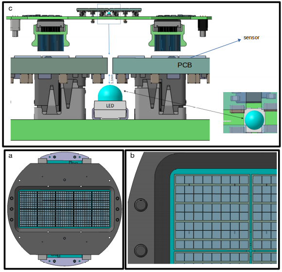
The FPA is designed to detect photons from both below and above the limb and consists of 10 SiPM arrays, each with pixels of mm2 (640 pixels in total). Each channel or pixel has a sensitive area of mm2. As it is known that a refractor and a Cassegrain optical system produce an inverted image when used without a diagonal mirror [24], the optical system of Terzina will image the Earth below the limb in the upper row of 5 SiPM arrays of the camera. These will be sensitive to eventual neutrino events from below the Earth’s limb, though the expected rate is negligble in Terzina. A larger mission will be required. They will be used for characterization of luminous noise from the Earth. The lower row of 5 SiPM arrays will observe EAS generated by UHECRs from above the limb. The telescope’s FoV is horizontally and vertically, as each pixel sees . A computer assisted design (CAD) model of the Terzina telescope is shown in figure 2 (on the left) and details of the CAD of the FPA and the tiles are shown on the right.
3 The NUV-HD-MT SiPMs for Terzina
The requirements for the SiPM technology to be adopted by Terzina are:
-
1.
to achieve PDE at 400 nm, namely in the region of the peak of the Cherenkov light spectrum (which for Terzina depends on the altitude of the EAS, but for the bulk of the events at around 30 km is between 350-500 nm);
-
2.
cross-talk of less than 10% at the operation voltage;
-
3.
dark count rate (DCR) of less than 100 kHz/mm2 at BoL of the mission.
-
4.
signal duration of less than 40 ns full width half-maximum (FWHM).
In partnership with FBK, we have selected their technology minimizing the cross-talk and the DCR, the NUV-HD-MT [25]. We then investigated the micro-cell size that maximize the PDF while keeping the signal duration short. In fact, the signal duration is proportional to the micro-cell size and its capacitance. A large signal increases the noise captured within the acquisition window required to integrate the full pulse. The NUV-HD-MT technology has been developed by FBK adding metal-filled Deep Trench Isolation (DTI) to strongly suppress optical cross-talk. Compared to NUV-HD, FBK finds a reduction in cross-talk by a factor of 10 [26]. We have measured the NUV-HD-MT SiPM of mm2 and mm2 with square micro-cell sizes of 25, 30, 35, 40, 50 . A further significant consideration is whether to utilise bare or coated sensors. While bare sensors require meticulous handling, the electrons may radiate Cherenkov light within the covering resin layer (see section 8).
3.1 Static characterisation
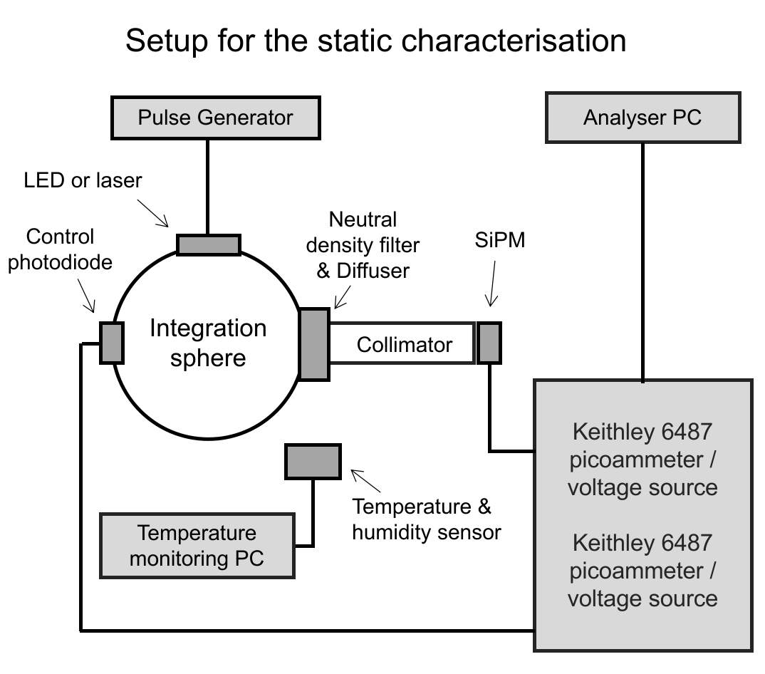
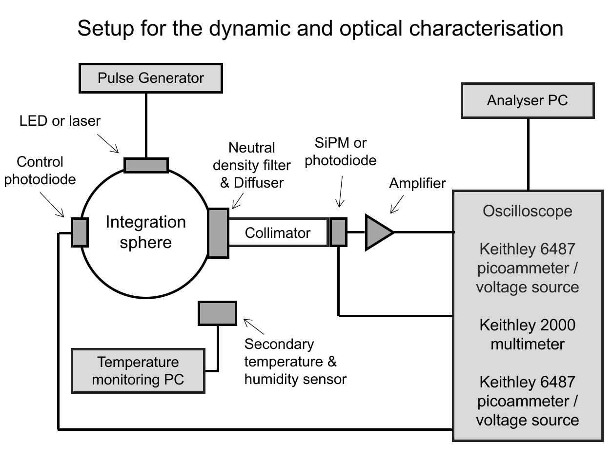
All the laboratory measurements have been performed at the University of Geneva, according to the setup and analysis methodology described in [4, 27]. Figure 4 shows the schematic layouts of the experimental setups for static (left) and dynamic/optical characterization (right).
The static characterisation and the forward IV measurements have been conducted to estimate the quenching resistance, while the reverse IV measurements have been used to determine the breakdown voltage.
The two configurations incorporate the following elements:
-
•
Pulsed LED with 450 nm wavelength, powered by a pulse generator operating at the frequency of 10 kHz. This creates alternating intervals: one where the device operates in complete absence of light and another where it is illuminated by the LED light (synchronized with the trigger waveform acquisition), during which photon signals are expected. Hereafter, these time intervals are referred to as dark interval and trigger window, respectively.
-
•
Integration sphere, used to eliminate any spatial variations in the incoming light by multiple scattering reflections on its internal surface. This ensures a uniform diffuse light output and preserves the power at each output port.
-
•
Neutral density filter, is inserted between the integration sphere output port and SiPM. For an automated switch between each filter, it is mounted on a motorized wheel. This enables us to illuminate the SiPMs with different light intensities as needed.
-
•
Diffuser, is inserted right after the neutral density filter to further reduce any residual non-uniformity from the output port of the integration sphere inside the collimator leading to the sensors.
-
•
Control photodiode, it is mounted at another output port of the integration sphere to monitor the amount of the inserted light within the setup at all times. This is connected to a Keithley 6487 picoammeter111The Keithley 6487 picoammeter is able to perform measurements of the current with precision of around 6.4 pA for currents lower than 2 nA./voltage source [28].
-
•
Temperature and humidity sensor, inserted near the SiPM and monitors the temperature constantly during the measurement.
-
•
Analyser PC, which monitors and logs the output from all measurement devices.
For the static characterization configuration, the IV curve was measured by directly biasing and reading the SiPM using a Keithley 6487 or Keithley 2400 [29] picoammeter/voltage source. In the dynamic characterization configuration, the bias voltage was supplied by a Keithley 6487 picoammeter/voltage source reading before the signal with a 2 GHz bandwidth oscilloscope. A custom-made amplifier with a bandwidth of approximately MHz and a gain of dB was used to amplify, pulse shape and filter the SiPM signal, and effectively suppressing the slow component of the SiPM response. The Keithley 2000 multimeter [30] shown in this configuration is used for reading a temperature sensor mounted near the control photodiode. The average temperature during the measurements was ∘C (hereinafter referred to as room temperature).
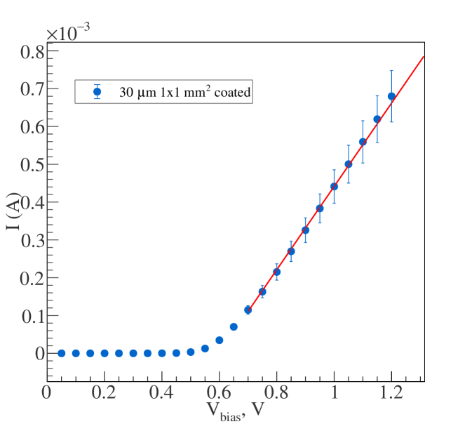
3.1.1 Forward IV characterisation
The forward IV characteristic curve of the FBK SiPMs, shown in figure 5 (left panel), exhibits a very small increase in current when the polarization voltage, , is below the threshold value, followed by a rapid, linear increase in current with above this threshold. This behaviour can be described by the Shockley law, which governs the forward current , flowing through a junction diode. A SiPM is an array of -cells () connected in parallel, each referred to as a SPAD (single photon avalanche diode). Each -cell can be modelled as a diode in series with a quenching resistor, . For the entire device, the voltage can be expressed as:
| (3.1) |
Here, is the ideality factor (ranging from for pure diffusion current and for pure recombination current), is the total reverse bias saturation current, is the thermal voltage, typically [27] and is the total forward current flowing through the SiPM. When the current is high (A), the last term becomes dominant. In this regime, the quenching resistance can be determined from a linear fit of the forward IV characteristic curve, as shown in figure 5 (red curve). The measured values of the quenching resistance are shown in table 1 (1000 k) for both bare and coated sensors of the same size but with varying micro-cell dimensions.
| sensor area (mm2) | cell size (m) | (k) | (V) | Coating |
|---|---|---|---|---|
| 25 | no | |||
| 35 | no | |||
| 25 | yes | |||
| 30 | yes |
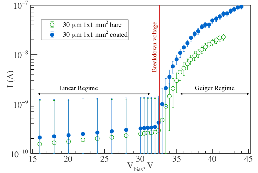
3.1.2 Reverse IV characterisation and IV model for post-breakdown
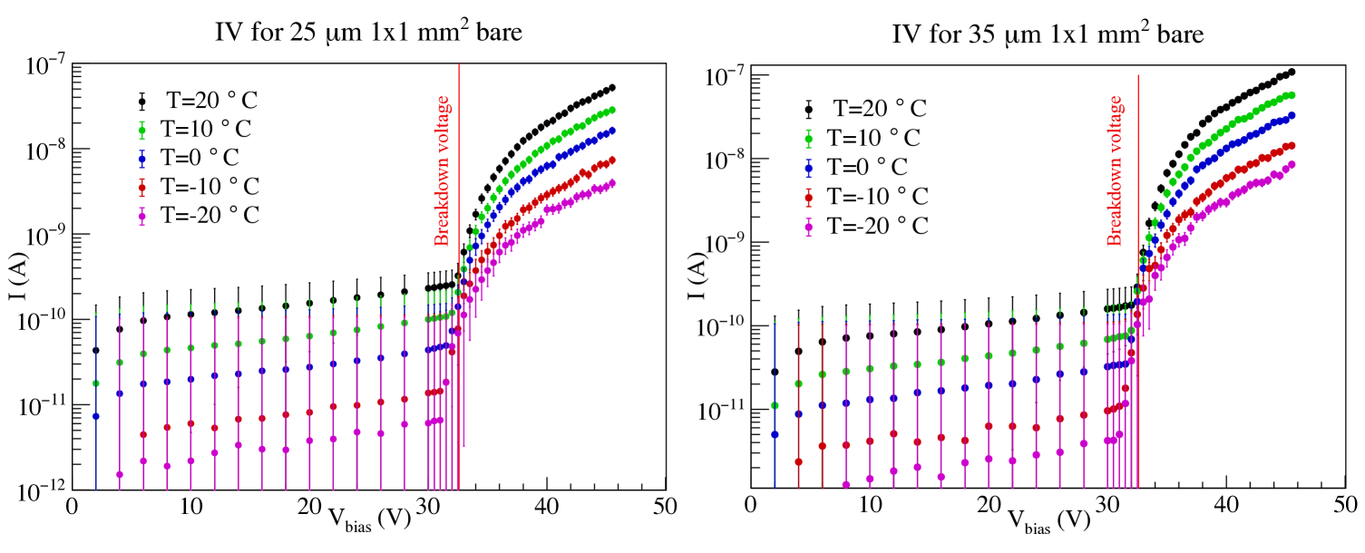
The reverse IV characteristic curve of the SiPM sensors is shown in figure 5 (right panel). The breakdown voltage, , has been calculated by using the second log-derivative method [31]. The results, presented in table 1, indicate that is approximately 32.6 V at room temperature for all cases.
In the reverse IV curves, two distinct regimes can be observed: the pre-breakdown “linear” regime and the post-breakdown Geiger regime, as illustrated in figure 5. This work employs the so-called “IV model” [32, 27], which describes the behaviour of SiPMs over their complete operating range, including the Geiger regime. The IV curves for all temperatures and devices exhibit similar behaviour as it is shown in figure 6, indicating multiple regimes of bias voltage. Taking all contributions into account, the post-breakdown current, , can be expressed as222The formula does not include the pre-breakdown term.:
| (3.2) |
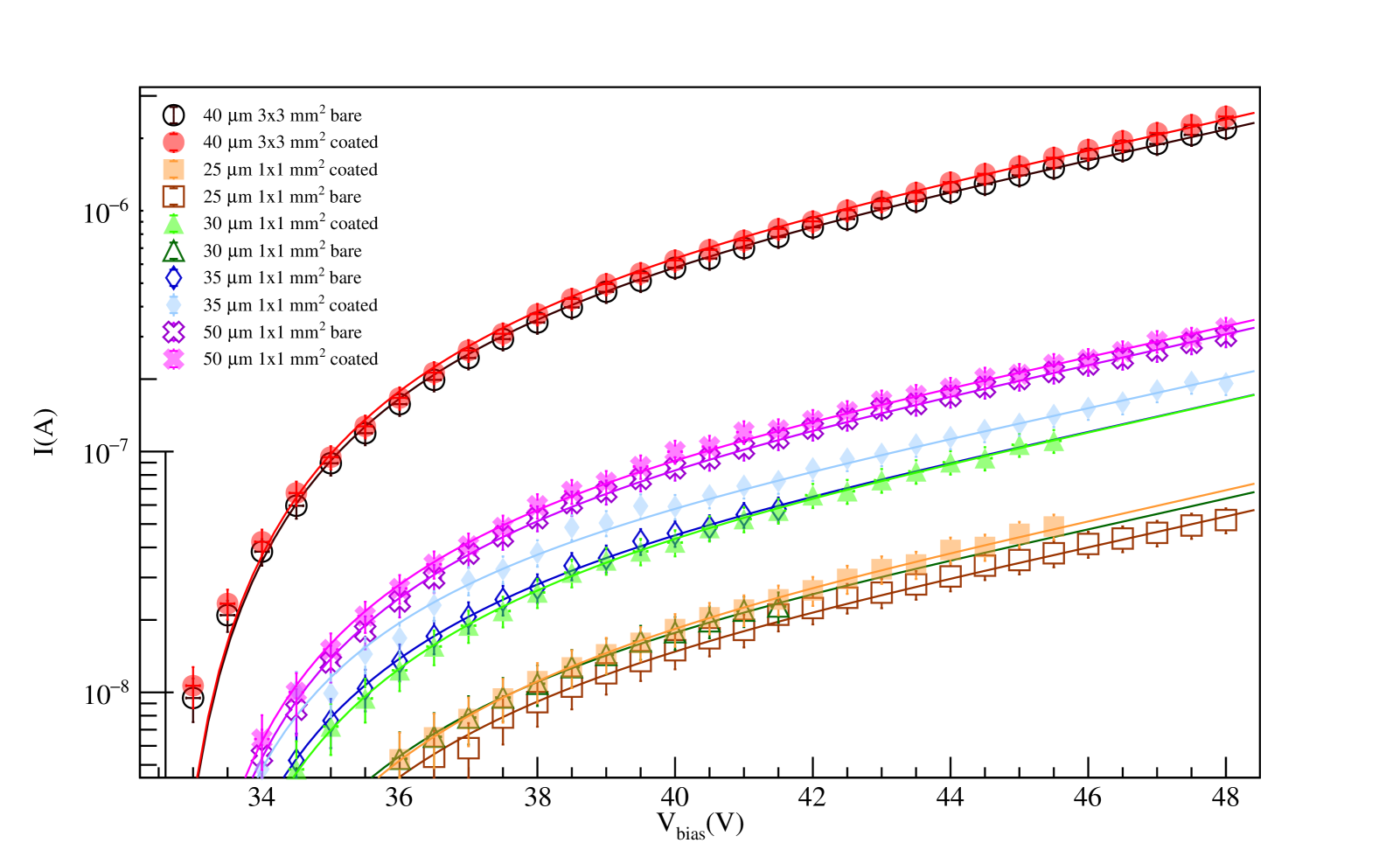
where corresponds to the contribution of the carrier-induced current, denotes the voltage where the after-pulses probability is one, is the breakdown voltage, is the capacitance and is related to the Geiger probability. They are free parameters of the model. The has been estimated with the second log-derivative method and it is a fixed value in the fit. This formula has been used to fit the experimental IV characteristics as shown in figure 7, and the corresponding fit values are summarized in table 2. This model will be used in the next sections to predict IV behaviour without repeating measurements.
| sensor size | cell size | |||||
|---|---|---|---|---|---|---|
| mm2 | 25 m coated | |||||
| mm2 | 30 m coated | |||||
| mm2 | 35 m coated | |||||
| mm2 | 50 m coated | |||||
| mm2 | 25 m bare | |||||
| mm2 | 30 m bare | |||||
| mm2 | 35 m bare | |||||
| mm2 | 50 m bare | |||||
| mm2 | 40 m bare | |||||
| mm2 | 40 m coated |
3.2 Dynamic characterisation
To understand and parametrise the dynamic behaviour of the SiPMs for our application, we analysed two categories of noise:
-
1.
Primary uncorrelated noise (dark count rate, DCR)
This noise is independent of the light conditions. At room temperature, the DCR is predominantly caused by the thermal generation of carriers. These carriers, under the operational voltage (), and influenced by the trap-assisted tunnelling effect, transition from the valence band to the conduction band, resulting in spurious signals. The increase in the DCR as a function of , due to the heightened electrical field, can be modelled by the empirical formula:(3.3) where is the rate of generated carriers at the given temperature, represents the probability that a generated carrier reaches the high-field region and triggers an avalanche (Geiger probability for dark pulses), and is a free parameter depending on the impact of .
-
2.
Secondary correlated noise
This noise arises from secondary avalanches occurring within the same or neighbouring micro-cells and can be categorized into:-
•
Prompt optical cross-talk (OCT): triggered by photons emitted during the primary avalanche multiplication process due to hot carrier luminescence.
-
•
Delayed optical cross-talk: caused by diffuse charge carriers created by photon absorption in non-depleted regions, which then drift through the depleted region.
-
•
After-pulsing (AP): triggered by carriers trapped in the micro-cell’s junction depletion layer during the primary avalanche and released after some delay.
In waveforms, prompt and delayed cross-talk appear as an increase in signal (doubling or more) in neighbouring micro-cells. In contrast, after-pulsing manifests within the same micro-cell and is strongly dependent on the recovery time of the SiPM micro-cells.
-
•
To perform the dynamic characterisation of SiPM and measure the uncorrelated noise, we utilized the setup shown in the right panel of Figure 4. A full over-voltage scan was conducted by ranging the voltage betweem 1 V and 18 V, and by acquiring 10’000 waveforms on the oscilloscope for each given over-voltage. To compute the DCR and OCT, the analysis specifically focused on the signals received within dark interval of the waveform (in the absence of light).
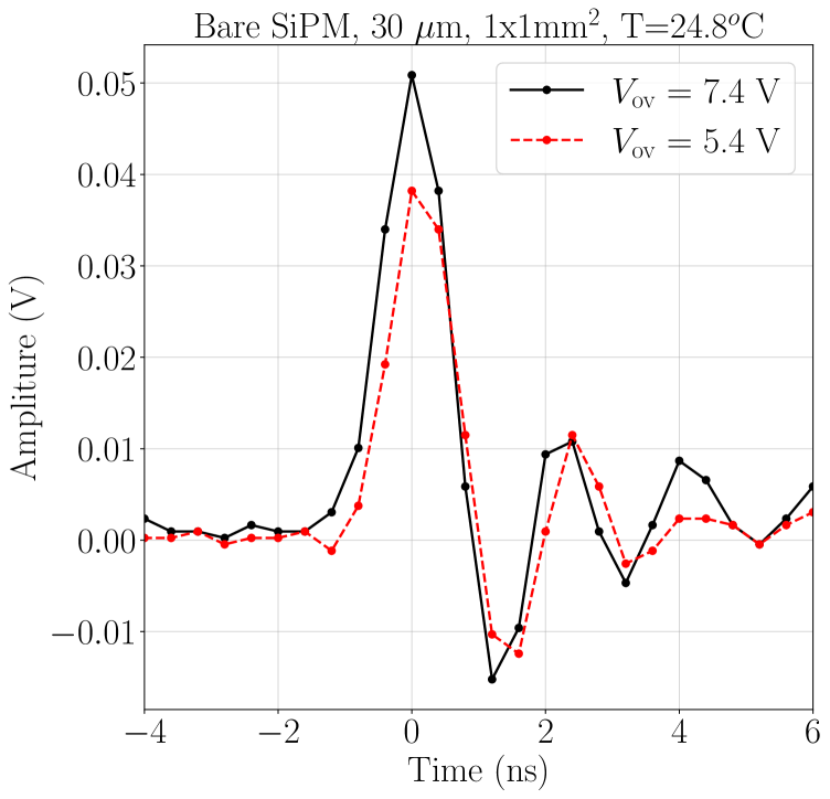
Figure 8 shows a typical single photoelectron signal at the over-voltage of 7.4 V and 5.4 V with full width half-maximum (FWHM) of about 1 ns and amplitudes of 50 mV and 40 mV, respectively. To determine the OCT, we considered the rate of accidental pile-up of 2 or more pulses within the same dark interval. A custom-made amplifier with a bandwidth of MHz and a gain of dB has been used for dynamic and optical characterisations. It performs pulse shaping and filtering, effectively cancelling the slow component of the SiPM response.
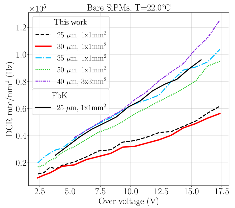
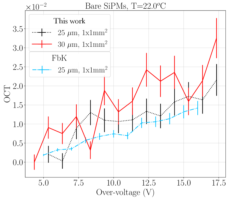
The results for the DCR and OCT are shown in figure 9 in the left and right panels, respectively. At 10 V over-voltage, the DCR per mm2 is less than 60 kHz for all the -cell sizes and the OCT is less than for 25 and 30 m. Because the OCT is quite small and statistics is limited, the errors are large for our measurements. Our measurements are compared to FBK ones which have a better precision. In addition, our laboratory is close to the RTS radio-television, and affected by a background at their frequencies (DAB at 223.936 MHz). Hence, we had to screen it by adopting a Faraday cage, but some noise can still be picked up by the cables. Overall, the measurements are in agreement.
3.3 Optical characterisation
The photon detection efficiency (PDE) is a crucial property of SiPMs, quantifyng how effectively the device detects incoming photons as a function of their wavelength (). The PDE can be described as:
| (3.4) |
Where is the quantum efficiency, i.e. the probability that a photon generates an electron-hole pair, is the fill factor, representing the percentage of the sensor area sensitive to light333The fill factor is influenced by the -cell sizes and their effective area at the pixel level. Specifically, the fill factor depends on how much of the total pixel area is occupied by the -cells compared to non-active regions (such as gaps or interconnects) within the pixel. and is the Geiger probability. The PDE strongly depends on the wavelength of the incident light, the over-voltage, and consequently, the breakdown voltage. In addition, PDE is temperature-dependent, as carrier mobility increases with temperature, potentially leading to an increase in PG for a fixed over-voltage. However, at around room temperature, this effect is likely negligible. Nonetheless, if the over-voltage is not adjusted to compensate for temperature variations, PDE measurements will fluctuate along with the breakdown voltage.
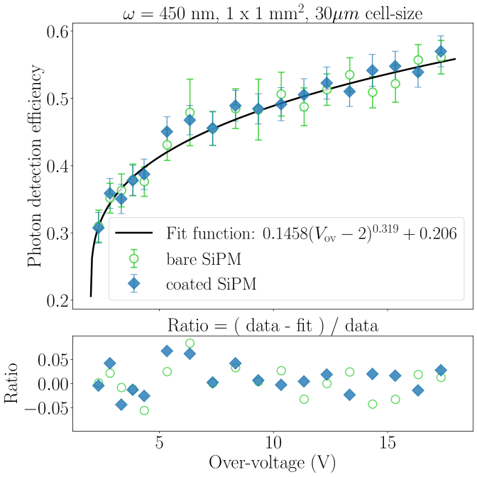
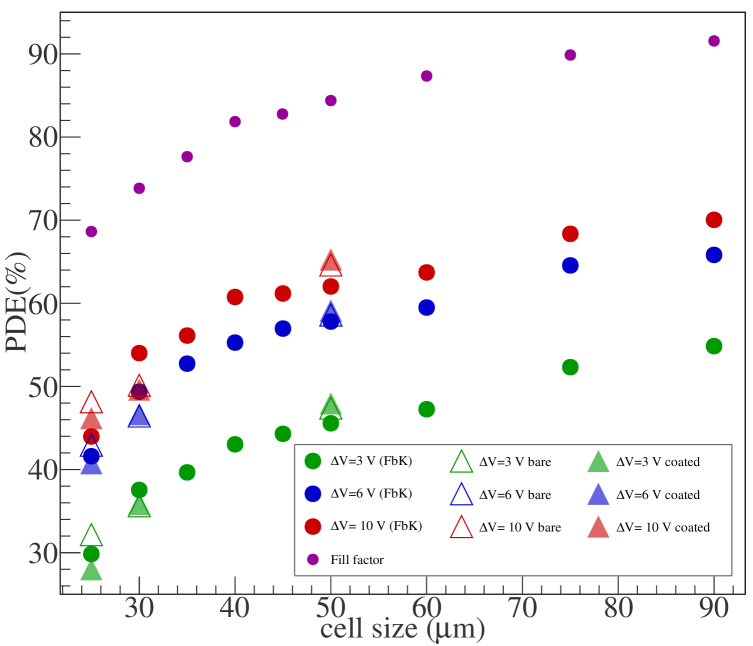
Using the same setup as in the dynamic characterization (right panel of Figure 4), we performed a calibration step by replacing the SiPM with a calibrated control photodiode to determine the absolute amount of incoming light. After reinstalling the FBK SiPM, we repeated the scan while illuminating it with a low-intensity pulsed LED. Following the analysis methodology of [27], we focused on the trigger window (the expected arrival time of photons from the LED). The PDE was calculated using the Poisson method, based on the average number of detected photons and corrected for uncorrelated SiPM noise. Figure LABEL:fig:pde_all_b shows the PDE as a function of the cell size for different over-voltages and sensor coatings. By looking at this plot and considering the results of the OCT and DCR, the 30 m cell size bare sensor appears to be the best solution for a LEO satellite. At 10 V of over-voltage, in fact, the PDE for 30 m cell size is already more than 50 (see figure LABEL:fig:pde_all_a).
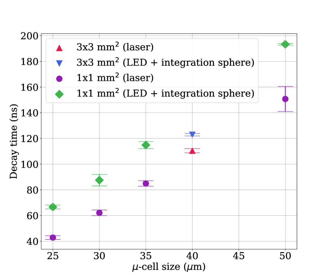
Weighing the DCR and PDE, as described above, against the pulse shape as outlined in [8], it has been decided to use SiPM tiles with a 30 m bare -cell size. At this configuration, we have an optimal performance in DCR and PDE, whilst still having a short pulse decay time. The decay time and the PDE are anti-correlated: smaller -cell sizes result in shorter signal durations but also in lower PDE due to the reduced fill factor. Hence, the final choice of the SiPM -cell of 30 m represents a trade-off between these parameters. Additionally it complies with the constraints on the maximum power consumption of the NUSES satellite. As a matter of fact, the larger the DCR, the larger the power consumption of the SiPM power supplies. If the data acquisition thresholds are not adjusted consequently, the rate of noise induced triggers would also require more processing activity further contributing to the increase in power consumption. We performed a set of measurements with three different configurations: 1) with a pulsed LED (450 nm) and an integration sphere; 2) with a short-duration (25 ps) light-pulse laser with a 370 nm wavelength laser with and 3) without the integration sphere. Both the LED and the laser flash the full sensor to obtain a high amplitude signal to be detectable by a 2 GHz bandwidth oscilloscope. Figure 11 summarizes the obtained results. As expected, the shortest decay time was measured with the laser only, as the integration sphere induces an additional time spread. The SiPM signal tail has been fitted with a negative exponential function and the decay time is in the figure. This time is a function of the -cell capacitance, hence its size. We did not observe any significant change in the signal shape with the variation in the bias voltage.
4 Evaluation of radiation fluxes for a LEO space mission
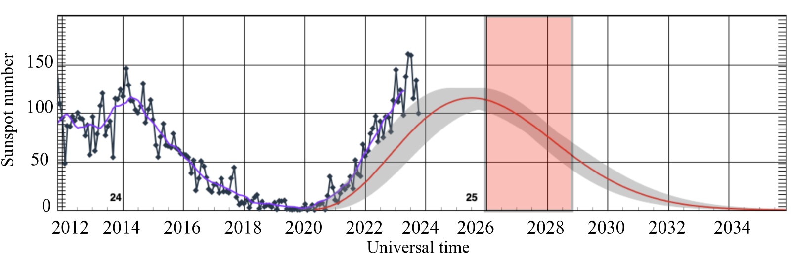
In order to evaluate the radiation damage in space on the sensors of the FPA, we use the SPENVIS (Space Environment Information System) [20] algorithm, a powerful software suite developed by the European Space Agency (ESA). In this framework, we built a project according to the specification of our mission’s orbit altitude of 550 km and an inclination of approximately between mid-2026 to mid-2029, which corresponds to an intense solar activity (see figure 13).
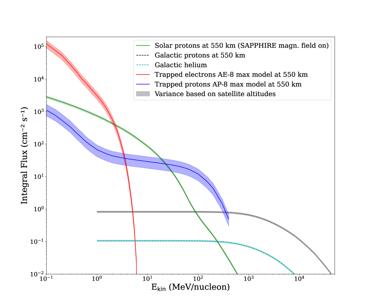
To estimate the total radiation we considered solar particle events (SPEs), trapped protons and electrons in the Van Allen radiation belts and galactic cosmic rays (GCRs). These expected fluxes for the NUSES spacecraft averaged on 15 orbits (1 day) during its operation time are shown in figure 13. The shaded areas indicate the fluctuations of these fluxes depending on the variation of the satellite altitude between 500 and 600 km and considering a period of maximum solar activity. In particular, the higher the altitude, the higher the flux of trapped protons and trapped electrons and consequently the slightly higher the flux of solar protons. Since the flight will occur during the declining part of the solar maximum, the fluxes for the trapped protons and electrons have been calculated using the NASA models AP-8 max and AE-8 max [35, 36], respectively, and the solar protons using the magnetic shield on in SAPPHIRE [37], and ISO 15390 model [38] for the GCRs. We used the realistic case of 550 km. It can be noticed that, for our altitude, the GCR contribution (protons and helium nuclei)444Heavier nuclei than p GCR fluxes are much lower at these energies and are neglected in this analysis. is negligible. Moreover, since NUSES will operate during intense solar activity, the solar flux will be very high while the galactic proton flux will be reduced [39] as the solar wind impedes GCR penetration into the solar system. The main contributions to the radiation damage to the camera will be due to trapped protons and electrons, and solar protons.
5 Dose estimates from radiation in space with Geant4
To estimate the dose that we expect on Terzina’s camera, we simulated the geometry of the telescope in Geant4. The simulated mechanics has small differences with respect to the final mechanics defined subsequently, but the few changes are irrelevant for this study. The simulated geometry, similar to the CAD in figure 2, includes:
-
1.
an external baffle or tube made of carbon fibre that covers the full telescope;
-
2.
a holder made of carbon fibre composed of a small baffle and a tower that protects the secondary mirror;
-
3.
different vanes made of carbon fibre;
-
4.
the focal plane composed by the sensors and the PCB connecting the tiles to the rest of the data acquisition system;
-
5.
the optical bench below the PCB (in aluminium and titanium);
-
6.
the aluminium radiators.
We tested different geometrical configurations varying the thickness and height of the external baffle and the thickness of the small baffle, indicated in Fig. 2. In particular, we report the results for three configurations: the hereafter called baseline geometry, with an external baffle of thickness of 1 mm and maximum height of the transverse section of 730 mm and the small baffle of 1 mm thickness; the same external cut baffle and a small baffle 4 mm thick, called benchmark configuration; a better shielded configuration, called shielded, consisting of a cylindrical external baffle 2 mm thick and of height 730 mm without a transverse cut, and a small baffle 4 mm thick.
Protons and electrons have been injected into these geometries simulated in Geant4 to estimate the total radiation dose. Particles were simulated in small energy bins considering the full energy range of the flux calculated with SPENVIS integrated over a sphere of radius cm surrounding the considered volumes and for the duration of the mission of 3 years. The total energy deposited in the sensitive volume of the FPA tiles and in the PCB, returned in MeV, has been calculated by Geant4. The total dose released in the corresponding volumes for all particles in the energy bin has been calculated summing all the differential doses:
| (5.1) |
returned in J/kg or gray, which is the SI unit of ionizing radiation dose defined as the absorption of 1 J of radiation energy per kg the object. We account for the fact that each particle crosses the spherical volume from the two opposite sides of the sphere by dividing by 2 in eq. 5.1, assuming that volumes have a uniform density and that is their total mass (sensors or PCB), and the conversion factor from MeV to Joule. These total doses for a 3-year mission, released in the simulated Terzina geometries by trapped electrons and protons, and solar protons are summarized in table 3. Considering these results, the shield power and the allowed weight for the mission, the benchmark configuration has been chosen for implementation, as the shielded one would not be affordable for weight limitations.
| Trapped (Gy) | Trapped (Gy) | solar (Gy) | ||
|---|---|---|---|---|
| baseline | sensors | |||
| PCB | ||||
| benchmark | sensors | |||
| PCB | ||||
| shielded | sensors | |||
| PCB |
6 Radiation damage in silicon with proton irradiation
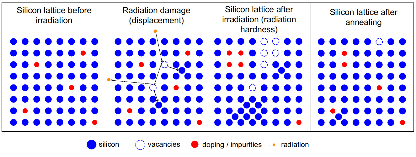
After the full characterisation of the sensors in section 2, we have irradiated them with protons and electrons in order to estimate the radiation damage. When an energetic charged particle hits a SiPM, it deposits energy through both ionizing and non-ionizing processes. Radiation damage of SiPMs has been extensively discussed in [40]. In silicon, bulk damage is due to Non-Ionizing Energy Loss (NIEL) and surface damage by Ionizing Energy Loss (IEL). Bulk damage is due to high energy particles (can be protons, neutrons, electrons, pions or photons) which can displace atoms out of their lattice creating defects as shown in figure 14. At energies beyond the keV scale, cluster defects can form when more atoms are displaced. Electrons beyond energies of 1 MeV typically can produce single defects, whereas heavier particles like protons produce also cluster defects. In the NIEL hypothesis, the radiation damage is proportional to the non-ionizing energy loss of the particles and this energy loss is proportional to the energy used to dislocate the lattice atoms (displacement energy). The defects in silicon crystals lead to an increase in leakage current due to the generation of electron-hole pairs from defects in the depletion region and trap-assisted tunneling. This leads to a temperature-dependent increase in DCR, which is more significant for protons than for electrons, which primarily induce ionisation rather than defects due to their lower mass and less efficient energy transfer to the crystal lattice, resulting in a minimal increase in DCR. A detail computation of the NIEL for protons and electrons in silicon can be done on Screened Relativistic (SR) Treatment for NIEL Dose Nuclear and Electronic Stopping Power Calculator [41]. Hence, we expect that damage caused by electrons induce a lower increase of the DCR when compared to protons at equal over-voltage, temperature, cell sizes, and dose.
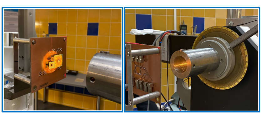
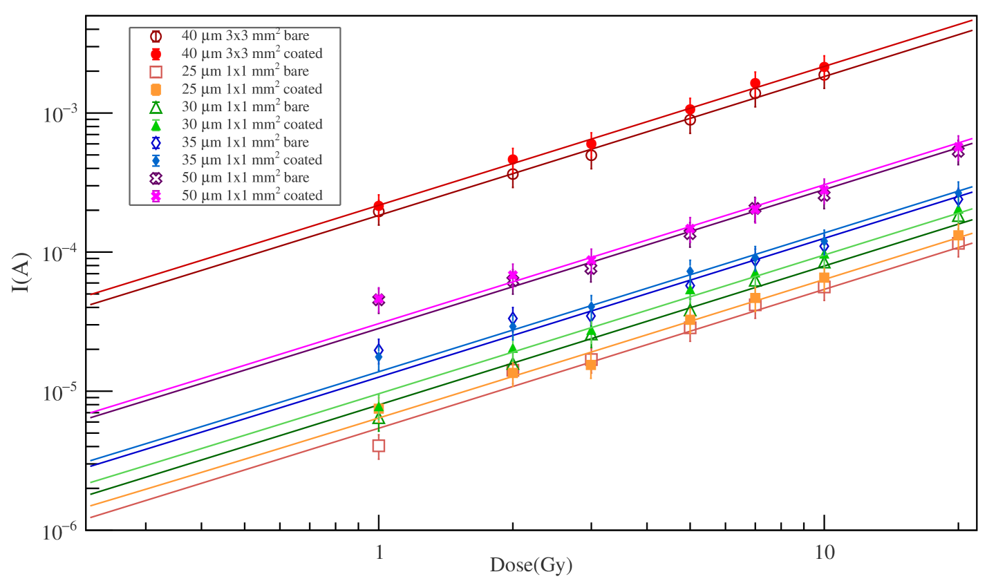
We performed the proton irradiation tests at the IFJ PAN in Krakow [42] with a 50 MeV proton beam (see the experimental setup in figure 15). The proton beam spot had a circular shape with a 35 mm diameter and homogeneity better than 5% with respect to the mean fluence. We measured the currents for mm2 SiPMs with -cell size of 25 , 30 , 35 and 50 and 33 mm2 SiPMs with a -cell size of 40 with and without resin coating. We measured the current of the SiPMs as a function of the bias voltage in the post-breakdown Geiger regime. The currents have been acquired just before the start of and during the irradiation process are shown as a function of the dose for the different devices in figure 16. The expected linear behaviour has been fitted as:
| (6.1) |
where the fit parameters, and , are reported in table 4 for V. The empirical model obtained from the fit will be used to predict the increase of the DCR as a function of dose in section 9.1. Variations of other SiPMs features, such as breakdown voltage and quenching resistance, have not been observed after irradiation.
| sensor size | cell size | (A) | (A/Gy) |
|---|---|---|---|
| mm2 | 25 m coated | ||
| mm2 | 30 m coated | ||
| mm2 | 35 m coated | ||
| mm2 | 50 m coated | ||
| mm2 | 25 m bare | ||
| mm2 | 30 m bare | ||
| mm2 | 35 m bare | ||
| mm2 | 50 m bare | ||
| mm2 | 40 m bare | ||
| mm2 | 40 m coated |
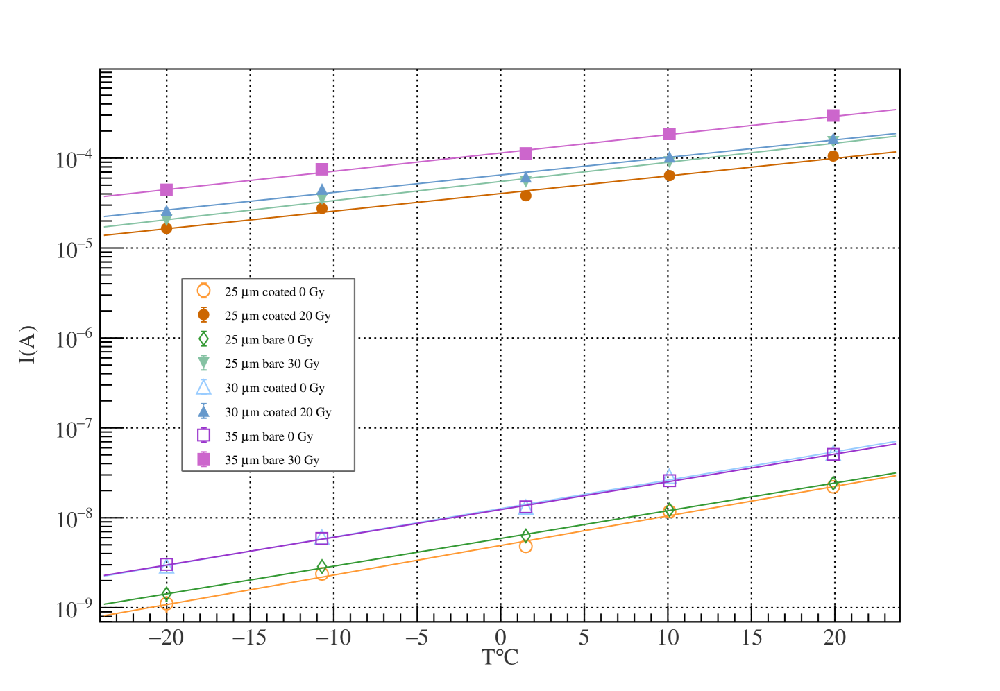
7 Thermal effect
To characterize the behaviour of the sensors as a function of temperature, we measured IV curves at different temperatures and extrapolated the DCR based on these curves. DCR being proportional to the post-breakdown current at a given over-voltage, we can derive the DCR from the current measurements. The results are used to select the sensor and set the operating temperature. Tests were performed both before and after irradiation. The temperature dependency of the IV curve measurements is modelled with the function, with parameters and :
| (7.1) |
The fit results are reported in table 5 and the measurements and the fit curves are shown in figure 17. It can be noted that the obtained parameter corresponds to the current at and the rate constant related to the exponential temperature constant provides the temperature correction factor used to obtain the currents at the desired temperature throughout this work. We can estimate the change in current per degree in order to get the temperature correction that we used in all the measurements. For example, we can estimate that, if the current value is doubled, the temperature will be obtained as as: . The current is doubled every 10 degrees before irradiation and every 15 degrees after irradiation (see last column in table 5). As shown in figure 17, the increase in DCR with temperature is slightly slower than in the presence of radiation.
| cell size | dose (Gy) | (A) | ||
|---|---|---|---|---|
| for double-current | ||||
| 25 m coated | 0 | |||
| 30 m coated | 0 | |||
| 25 m bare | 0 | |||
| 30 m bare | 0 | |||
| 35 m bare | 0 | |||
| 25 m coated | 20 | |||
| 30 m coated | 20 | |||
| 25 m bare | 30 | |||
| 35 m bare | 30 |
As in section 2, we estimated the breakdown voltage using the second log-derivative method. We found that the breakdown voltage changes linearly with temperature by about 30 mV per degree on average. We found a rate for the bare sensor of about 32 mV per degree and a rate of the 28 mV per degree for the coated sensor. On the other hand, the quenching resistance is not affected by the change in temperature.
8 Electrons irradiation measurements and simulations
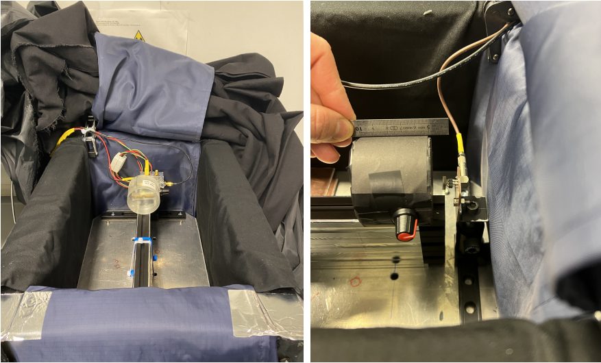
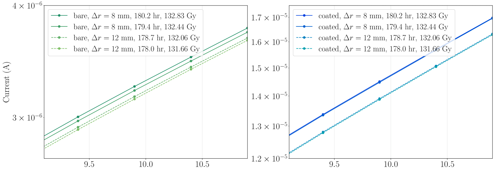
In order to measure the radiation damage effect on SiPMs, namely the increase of DCR due to electrons, and predict this effect during the NUSES mission, we used a strontium 90 () emitting source with activity of 16.75 MBq. Two bare and coated NUV-HD-MT of mm2 SiPMs with 40 -cell size and sensitive area were exposed to the source. All measurements are done in an over-voltage interval from 0 to 18 V. Considering the energy spectrum of primary and secondary electrons from decays [43], with this source we can study radiation damage from electrons up to a maximum energy of 2.28 MeV. As done for protons, we measured the current increase, but in this case we moved the source at different distances from the SiPM using the experimental setup shown in figure 18. We also built up a full simulation in Geant4 of this setup to compare with the measurements. Figure 19 depicts the measured current as a function of time at different over-voltages and changing the distance of the source from the SiPM as indicated on the top axis.
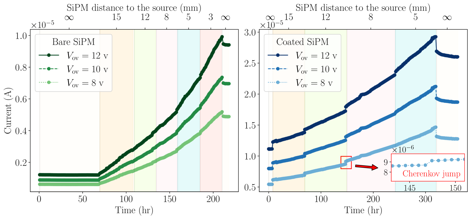
Figure 20 shows the same current as a function of over-voltage (IV curves) for the same sensors, with bare SiPM on the left panel and coated SiPM on the right panel. The time of irradiation for each IV curve is indicated in the label. First, we put the source at a 12 mm distance to the SiPM (lower dashed curves). It can be seen that the different times of exposure to the source introduce a small difference due to the electron radiation damage for different exposure times. Then we move the source to 8 mm distance to the SiPM and we again see that for different exposure times the effect on the IV curve is small between, but on the right panel for the coated SiPM there is a larger increase as we moved the source closer to the SiPM. This indicates that there is an additional contribution to the radiation damage of electrons which is due to the Cherenkov emission of electrons in the coating resin. As expected, this effect is not observed on the left panel for the bare SiPM.
The indicated doses in figure 20 are calculated as follows. The simulation provides us with the precise energy deposition () of electrons resulting from ionizing and non-ionizing processes as they pass through each layer of the SiPM. By dividing the silicon volume into 8 layers and running the simulation many times, we obtained the mean value of the total energy deposit in the volume of the SiPM, denoted as . We can then compare the or dose in each layer to analyse where most of the OCT and DCR contributed. Using the following formula, we calculate the dose () in each layer:
| (8.1) |
Here, , , and represent the charge of an electron, the activity of the source, and the mass of the silicon layer, respectively. It is worth noting that each simulation iteration corresponds to a single decay event of . Considering the source’s activity, this equation provides the equivalent of a per one second, and thus, we derive the dose rate in Gy/hr. Figure 21 shows the final dose from the simulation in each silicon layer of the SiPM.
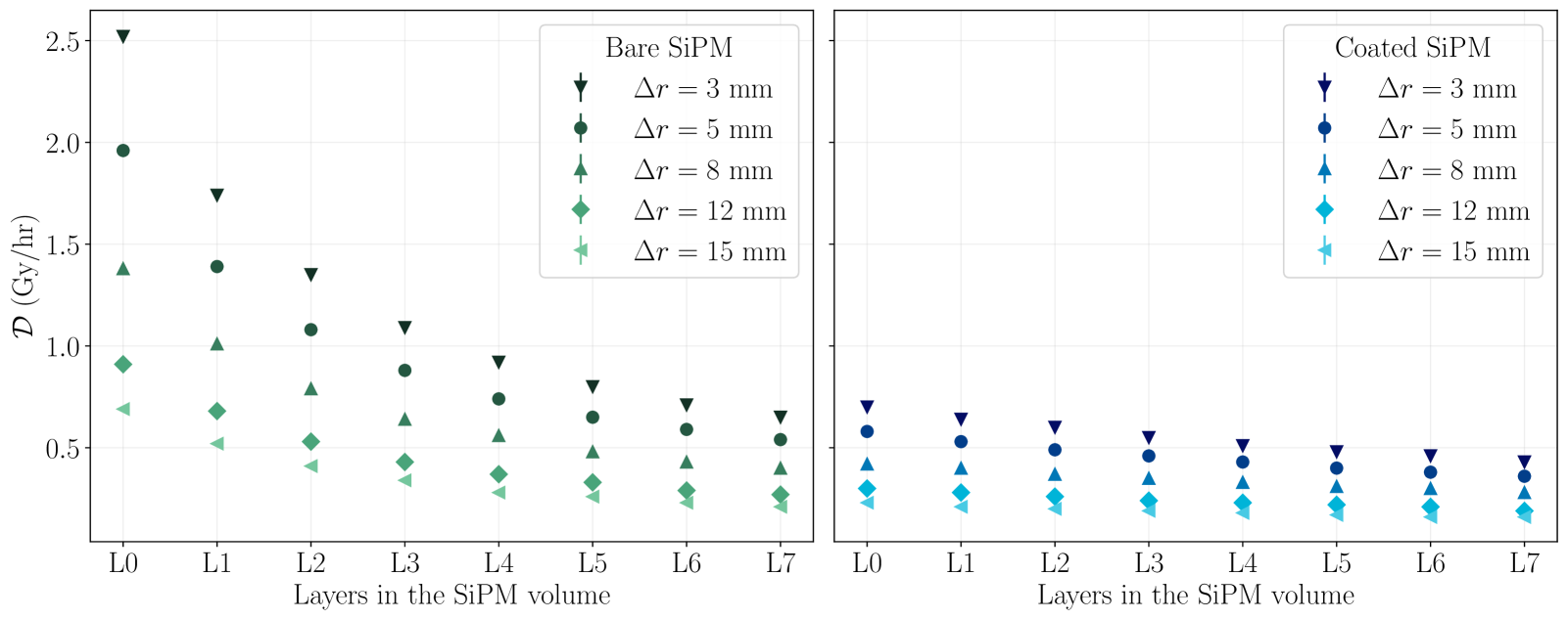
Overall, we use the final estimated dose as a function of time from simulation to estimate the irradiated dose at the time of IV measurements in figure 20. This will give us the expected current increase per received dose for the trapped electrons.
9 DCR prediction during mission
The DCR represents the baseline count rate in the absence of incident light. In order to avoid that the camera is constantly triggering on DCR induced events, the threshold of the trigger has to be increased with increasing DCR. This impacts the lowest achievable energy of the detected primary cosmic rays. With all the measurements that have been done for thermal response, electrons and protons campaigns, we can now calculate the DCR considering the overall effects through the following formula:
| (9.1) |
Here, the , , Gain, , , and stand for over-voltage ( V), effective sensitive area, gain of the SiPM in use, average operation temperature during the mission (C), dose released by either protons or electrons, and the electron charge, respectively.
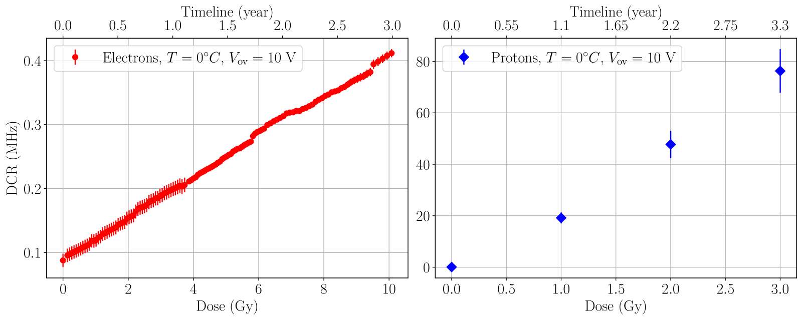
The corresponds to the measured current divided by , namely scaling for the ratio of areas to take into account the different SiPM sizes. The exponential term provides the measured current at desired temperature following the model in equation 7.1. Combining the DCR results with the dose-per-time response from the simulation yields the results in figure 22. As can be seen from the graph, the damage caused by electrons is very low when compared to protons at equal over-voltage, temperature, cell sizes, and dose as expected. Specifically, 2 Gy of electrons corresponds to a DCR of approximately 0.15 MHz, while 2 Gy from protons results in a DCR of around 50 MHz, starting from the same DCR at 0 Gy.
For this reason in the next section only the radiation damage produced by protons will be taken into account in the thermal annealing strategy done to recover the SiPM response.
9.1 Annealing
A mitigation strategy based on thermal annealing is proposed for addressing radiation damage of the sensors which causes DCR increase, then resulting in higher power consumption and higher energy threshold. This is a controlled thermal process used to improve the performance and stability of electronic devices, including SiPMs. During annealing, SiPMs are subject to elevated temperatures for a specific period, followed by gradual cooling. This process helps to repair structural defects and radiation-induced damage that affect the device’s performance. Additionally, annealing can reduce internal stresses in the semiconductor material, thereby improving the uniformity of the SiPM’s response and reducing background noise.
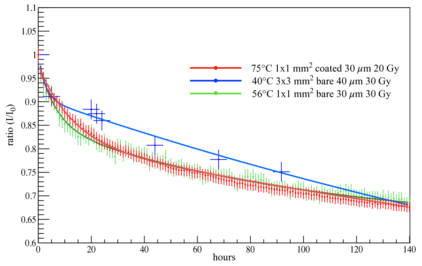
In the laboratory, we study the annealing effect by placing the irradiated devices in a climate chamber at a fixed temperature for a certain period and regularly measuring their IV curve. Then we measure again the current and compare it with the SiPM’s current before irradiation at the given over-voltage of 10 V to determine the recovery efficiency of the annealing process. The time evolution of the 10 V over-voltage current for different storage temperatures is shown in figure 23 for three types of SiPMs. In this figure the y-axis shows the normalized current to the current before irradiation and slightly to the irradiation level. The increase of current is equivalent to the DCR increase due to irradiation. It can be noticed that the current is following an exponential decay with time, whose amplitude, time constant, and offset varying with the storage temperature. The data points in figure 23 are therefore fitted with the following function:
| (9.2) |
whose fit parameters are reported in table 6. The exponential offset is linked to the fraction of the post-irradiation dark current that can be recovered after an infinite amount of time, while the exponential slope can be seen as a dark current recovery rate. Based on various measurements for different SiPMs at fixed temperatures, we concluded that at temperatures above and an annealing cycle of 84 hours, up to of the SiPM’s response current can be recovered.
| T (∘C) | sensor | (Gy) | (hr-1) | (hr-1) | ||
|---|---|---|---|---|---|---|
| 40 | 40 m bare 3x3 mm2 | 30 | ||||
| 56 | 30 m bare 1x1 mm2 | 20 | ||||
| 75 | 30 m coated 1x1 mm2 | 20 |
Using this information, we constructed a model to estimate the expected DCR in space due to accumlating irradiation and the planned annealing processes. These two components change the DCR during the mission and can be described by the following differential equation:
| (9.3) |
where and are numeric constants and the first and the second terms represent the irradiation and annealing contributions, respectively.
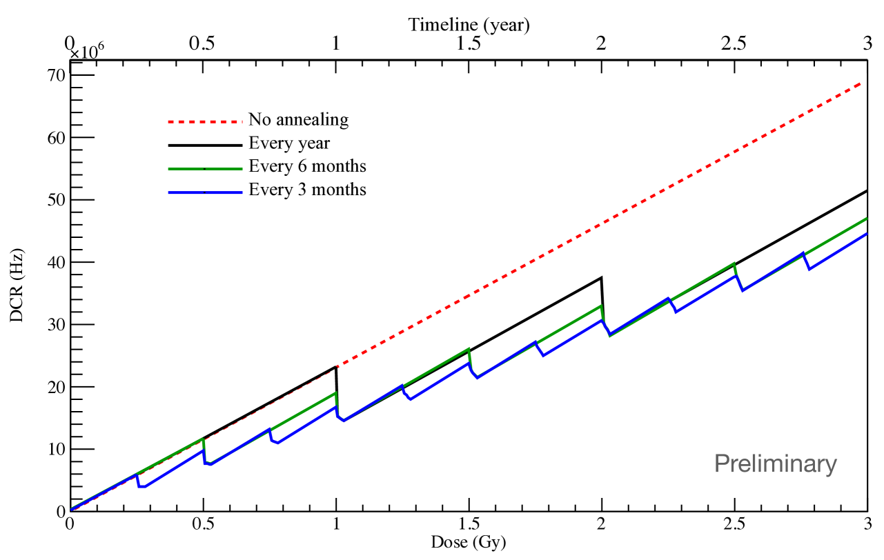
In absence of annealing, irradiation scenario, the solution of this equation is given by the linear increase in DCR as a function of the dose described in equation 6.1. During the annealing process, the solution of the equation is given by the exponential decay model described in equation 9.2. Note that over time, the effectiveness of annealing cycles decreases as the lattice becomes more rigid and less responsive to the heating treatment. Moreover, during the annealing cycle the FPA is still taking irradiation. Taking into account all these factors, the resulting DCR from proton irradiation as a function of time/dose for three different annealing strategies is shown in figure 24.
10 Conclusions
This work presents the characterisation of FBK SiPMs, which allowed to select the optimal size of the -cells of SiPMs to adopt in the Terzina mission, and the study that determines the power consumption increase with radiation damage. It also lead to the definition of a mitigation strategy based on periodic annealing during the mission. A model has been developed from the measurements which allows other users to determine similar mitigation strategies to this relevant damaging effect of SiPMs.
Acknowledgments
NUSES is funded by the Italian Government (CIPE n. 20/2019), by the Italian Ministry of Economic Development (MISE reg. CC n. 769/2020), by the Italian Space Agency (CDA ASI n. 15/2022), by the European Union NextGenerationEU under the MUR National Innovation Ecosystem grant ECS00000041 - VITALITY - CUP D13C21000430001 and by the Swiss National Foundation (SNF grant n. 178918). This study was carried out also in collaboration with the Space It Up project funded by the Italian Space Agency, ASI, and the Ministry of University and Research, MUR, under contract n. 2024-5-E.0 - CUP n. I53D24000060005.
References
- [1] D. Renker and E. Lorenz, Advances in solid state photon detectors, JINST 4 (2009) P04004.
- [2] F. Acerbi and S. Gundacker, Understanding and simulating SiPMs, Nucl. Instrum. Meth. A 926 (2019) 16.
- [3] T. Montaruli and A. Nagai, Properties of large SiPM at room temperature, Nucl. Instrum. Meth. A 985 (2021) 164609 [2001.06791].
- [4] A. Nagai, C. Alispach, D. Della Volpe, M. Heller, T. Montaruli, S. Njoh et al., SiPM behaviour under continuous light, JINST 14 (2019) P12016 [1910.00348].
- [5] NUSES collaboration, The NUSES space mission, PoS TAUP2023 (2024) 121.
- [6] L. Burmistrov, Terzina on board nuses: A pathfinder for eas cherenkov light detection from space, EPJ Web of Conferences 283 (2023) 06006.
- [7] NUSES collaboration, The NUSES space mission, J. Phys. Conf. Ser. 2429 (2023) 012007.
- [8] L.o.b.o.t.N.C. ”Burmistrov, A silicon-photo-multiplier-based camera for the terzina telescope on board the neutrinos and seismic electromagnetic signals space mission, Instruments 8 (2024) .
- [9] HERD collaboration, Overall Status of the High Energy Cosmic Radiation Detection Facility Onboard the Future China’s Space Station, PoS ICRC2019 (2020) 062.
- [10] F.C.T. Barbato, G. Barbarino, A. Boiano, R. de Asmundis, F. Garufi, F. Guarino et al., Crystal eye: a wide sight on the universe looking for the electromagnetic counterpart of gravitational waves, in UV, X-Ray, and Gamma-Ray Space Instrumentation for Astronomy XXI, O.H. Siegmund, ed., SPIE, Sept., 2019, DOI.
- [11] A. Olinto, J. Krizmanic, J. Adams, R. Aloisio, L. Anchordoqui, A. Anzalone et al., The poemma (probe of extreme multi-messenger astrophysics) observatory, Journal of Cosmology and Astroparticle Physics 2021 (2021) 007.
- [12] A.V. Olinto, POEMMA (Probe of Extreme Multi-Messenger Astrophysics) Roadmap Update, arXiv e-prints (2023) arXiv:2309.14561 [2309.14561].
- [13] T.J.-E. Collaboration, Joint Experiment Missions for Extreme Universe Space Observations (JEM-EUSO), 2024.
- [14] S. Bacholle et al., Mini-euso mission to study earth uv emissions on board the iss, The Astrophysical Journal Supplement Series 253 (2021) 36.
- [15] J.H.A.J. au2, L.A. Anchordoqui, J.A. Apple, M.E. Bertaina, M.J. Christl, F. Fenu et al., White paper on euso-spb2, 2017.
- [16] F. Bisconti, Use of Silicon Photomultipliers in the Detectors of the JEM-EUSO Program, Instruments 7 (2023) 55.
- [17] T.J.-E. Collaboration, EUSO-SPB2 News, 2024.
- [18] S. Mianowski, N. De Angelis, J. Hulsman, M. Kole, T. Kowalski, S. Kusyk et al., Proton irradiation of SiPM arrays for POLAR-2, Experimental Astronomy 55 (2023) 343 [2210.01457].
- [19] N. De Angelis, M. Kole, F. Cadoux, J. Hulsman, T. Kowalski, S. Kusyk et al., Temperature dependence of radiation damage annealing of Silicon Photomultipliers, Nuclear Instruments and Methods in Physics Research A 1048 (2023) 167934 [2212.08474].
- [20] Spenvis: The space environment information system, 2022.
- [21] Geant4: Toolkit for the simulation of the passage of particles through matter. its areas of application include high energy, nuclear and accelerator physics, as well as studies in medical and space science, 2019.
- [22] J. Allison, K. Amako, J. Apostolakis, P. Arce, M. Asai, T. Aso et al., Recent developments in geant4, Nuclear Instruments and Methods in Physics Research Section A: Accelerators, Spectrometers, Detectors and Associated Equipment 835 (2016) 186.
- [23] A. Neronov, D.V. Semikoz, L.A. Anchordoqui, J.H. Adams and A.V. Olinto, Sensitivity of a proposed space-based cherenkov astrophysical-neutrino telescope, Phys. Rev. D 95 (2017) 023004.
- [24] E.H. Linfoot, The Schmidt-Cassegrain systems and their application to astronomical photography, MNRAS 104 (1944) 48.
- [25] A. Gola, F. Acerbi, M. Capasso, M. Marcante, A. Mazzi, G. Paternoster et al., Nuv-sensitive silicon photomultiplier technologies developed at fondazione bruno kessler, Sensors 19 (2019) .
- [26] A. Gola, Status and perspectives of SiPM, 2022.
- [27] A. Nagai, C. Alispach, A. Barbano, V. Coco, D. della Volpe, M. Heller et al., Characterization of a large area silicon photomultiplier, Nuclear Instruments and Methods in Physics Research Section A: Accelerators, Spectrometers, Detectors and Associated Equipment 948 (2019) 162796.
- [28] U. Manual, “Series 6487 SourceMeter.” https://download.tek.com/manual/6487-901-01(B-Mar2011)(Ref).pdf, 2011.
- [29] U. Manual, “Series 2400 SourceMeter.” https://download.tek.com/manual/2400S-900-01_K-Sep2011_User.pdf, 2011.
- [30] U. Manual, “Model 2000 Multimeter.” https://download.tek.com/manual/2000-900_J-Aug2010_User.pdf, 2010.
- [31] A. Nagai, C. Alispach, A. Barbano, V. Coco, D. della Volpe, M. Heller et al., Characterisation of a large area silicon photomultiplier, Nucl. Instrum. Meth. A 948 (2019) 162796 [1810.02275].
- [32] N. Dinu, A. Nagai and A. Para, Breakdown voltage and triggering probability of SiPM from IV curves at different temperatures, Nucl. Instrum. Meth. A 845 (2017) 64.
- [33] F. James, MINUIT Function Minimization and Error Analysis: Reference Manual Version 94.1, .
- [34] The Space Weather Prediction Center, ISES Solar Cycle Sunspot number progression, 2025.
- [35] J.I. Vette, The nasa/national space science data center trapped radiation environment model program, 1964 - 1991, NASA-TM-107993 (NASA Goddard Space Flight Center Greenbelt, MD, United States) (1991) .
- [36] J.I. Vette, The ae-8 trapped electron model environment, NSSDC/WDC-A-RS-91-24 (NASA Goddard Space Flight Center Greenbelt, MD, United States) (1991) .
- [37] “Sapphire implementation instructions.”
- [38] “Iso 15390 gcr model.”
- [39] A.J. Tylka, J.H. Adams, Jr and P.R. Boberg, Creme96: A revision of the cosmic ray effects on micro-electronics code, IEEE Transactions on Nuclear Science 44 (1997) .
- [40] E. Garutti and Y. Musienko, Radiation damage of SiPMs, Nucl. Instrum. Meth. A 926 (2019) 69 [1809.06361].
- [41] P.R. M.J. Boschini and M. Tacconi, SR-NIEL–7 Calculator: Screened Relativistic (SR) Treatment for NIEL Dose, Nuclear and Electronic Stopping Power Calculator (version 10.16), .
- [42] J. Swakon, P. Olko, D. Adamczyk, T. Cywicka-Jakiel, J. Dabrowska, B. Dulny et al., Facility for proton radiotherapy of eye cancer at ifj pan in krakow, Radiation Measurements 45 (2010) 1469.
- [43] J.J. Devaney Tech. Rep. https://www.osti.gov/biblio/5143758 (08, 1985), DOI.