Noise-to-current ratio divergence as a fingerprint of dispersing Majorana edge modes
Abstract
The definitive detection of Majorana modes in topological superconductors is a key issue in condensed matter physics. Here we propose a smoking-gun experiment for the detection of one-dimensional dispersing Majorana edge modes, based on theoretical results for multi-terminal transport in a setup consisting of two normal metal leads and a topological superconductor. In the proposed device, the unpaired nature of the Majorana edge modes inherently leads to the absence of the charge current in the linear response regime, while the current fluctuation remains significant. Therefore, the divergence in the noise-to-current ratio serves as unambiguous evidence for the presence of the dispersing Majorana edge modes. We reach this conclusion analytically, without relying on any specific model of topological superconductors. In addition, using tight-binding models of topological-insulator-based topological superconductors, we numerically verify the predicted divergent noise-to-current ratio. We also discuss the application of our proposal to the CoSi2/TiSi2 heterostructure and the iron-based superconductor FeTe1-xSex.
I Introduction
Majorana modes in topological superconductors (TSs) [1, 2, 3, 4, 5] have become a central topic in condensed matter physics, due to their potential applications for fault-tolerant topological quantum information technologies. [6, 7, 8, 9, 10]. To date, the existence of Majorana edge modes (MEMs) has been predicted in various platforms, including semiconductor-superconductor hybrids [11, 12, 13, 14, 15, 16, 17, 18, 19], magnetic material-superconductor hybrids [20, 21, 22, 23], topological insulator-superconductor hybrids [24, 25, 26], CuxBi2Se3 [27, 28, 29], and iron-based superconductors [30, 31, 32, 33, 34, 35, 36, 37]. However, the unambiguous verification of MEMs in these systems remains a significant challenge [38]. Zero-bias conductance peaks observed in normal metal–superconductor junctions [39, 40, 41, 42, 43, 44] have long been regarded as a strong experimental signature of MEMs. Nevertheless, recent studies have shown that zero-bias conductance peaks can also arise from various factors unrelated to Majorana physics [45, 46, 47, 48, 49, 50, 51, 52], making their definitive identification difficult. This stalemate highlights the necessity of further experimental strategies for the unambiguous detection of MEMs.
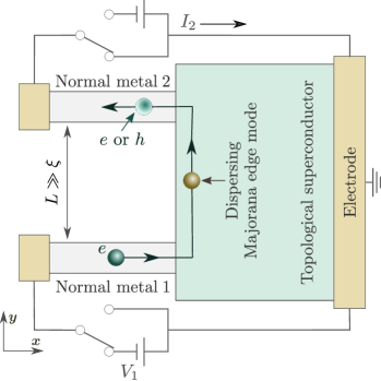
In this Letter, we propose a versatile experiment that provides a smoking-gun signature of the one-dimensional dispersing MEMs. The one-dimensional dispersing MEMs are particularly important because they can be harnessed in the braiding operations of topological computing [53, 54, 55]. To detect the dispersing MEMs, we measure the nonlocal charge transport [44, 56, 57, 58, 59, 60, 61] in a multi-terminal setup as shown in Fig. 1, where two normal metal (NM) leads are attached to one edge of a TS. When the distance between the NM leads () is sufficiently larger than the superconducting coherence length (), inter-lead scattering mediated by evanescent modes of conventional Bogoliubov quasiparticles vanishes completely [62]. Thus, the nonlocal charge current at bias voltages below the superconducting gap is carried exclusively by the MEM propagating along the edge. Importantly, in usual Bogoliubov quasiparticles, electron-like and hole-like modes exist in pairs at zero energy due to particle-hole symmetry. In contrast, the MEM, where particle and antiparticle modes are equivalent, can exist individually. We show that this unpaired nature of the MEM essentially leads to the absence of the charge currents in the linear response limit, while the current fluctuation remains significant. As a result, the divergence in the noise-to-current ratio at zero bias voltage serves as a smoking-gun signature of the dispersing MEM in the proposed setup. We reach this conclusion without relying on any specific model of the TS. Thus, we expect that the proposed experiment is useful to detect any one-dimensional dispersing MEMs, including Majorana hinge modes in three-dimensional second-order TSs [63, 64, 65, 66, 67]. To validate our theory more robustly, we also perform numerical calculations for specific tight-binding models of the superconducting topological insulator thin films [26, 37]. Finally, we discuss potential applications of our proposal to the CoSi2/TiSi2 heterostructure [68, 69] and the iron-based superconductor FeTe1-xSex [70, 71, 72, 73].
II noise-to-current ratio
Let us consider a two-dimensional hybrid system as shown in Fig. 1, where two NM leads are attached to an edge of a TS. We calculate the charge current at zero temperature within the Blonder–Tinkham–Klapwijk (BTK) formalism [62, 74]:
| (1) | ||||
where we assume . represents the time-averaged charge current in the -th NM due to the bias voltage applied to the electrode connected to the -th NM, where the electrodes attached to the -th NM and the TS are grounded (i.e., ). We denote the number of propagating channels in the -th NM by . The matrices of and ( and ) contain the scattering coefficients from an electron (a hole) in the -th NM to an electron and a hole in the -th NM at energy , respectively. In addition, we calculate the zero-frequency noise power based on the BTK formalism [75, 76],
| (2) |
with
| (3) | ||||
where represents the deviation of the current at time from the time-averaged current. In the BTK formalism, we assume that the currents flowing towards () are absorbed into the ideal electrode connected to the TS (NM), while these electrodes are not explicitly included in the Hamiltonian. The BTK formalism is quantitatively valid for bias voltages well below the superconducting gap.
In the following, we focus on the linear response limit , where the time-averaged current, , and the zero-frequency noise power, , are calculated using only the inter-lead scattering matrix at zero energy:
| (6) |
where we use the notation , for simplicity. Due to particle-hole symmetry of the superconducting system, the scattering matrix satisfies [77]
| (7) | ||||
where is the null matrix, denotes the identity matrix, and represents the complex conjugation operator. Therefore, we obtain
| (8) |
We rewrite the scattering matrix in a Majorana representation, transforming into a real matrix [77]:
| (11) |
where . Using singular value decomposition, we represent the scattering matrix as
| (12) |
where is the real diagonal matrix, () is the real orthogonal matrix satisfying ().
Here we assume , where is the distance between the two NM leads and is the superconducting coherence length. In this limit, the inter-lead scattering mediated by evanescent modes of the Bogoliubov quasiparticles vanishes completely [62]. In addition, we assume that only one dispersing MEM mediates the inter-lead scattering from the -th NM to the -th NM, as shown in Fig. 1. These assumptions lead to [77]
| (13) |
Note that for conventional Bogoiubov quasiparticles, the electron-like and hole-like modes exist in pairs at zero energy due to particle-hole symmetry, which results in an even rank for . Therefore, the relation of is a clear manifestation of the unpaired nature of the MEM. For a TS belonging to class D of the Altland-Zirnbauer symmetry class [78], we specifically assume a topological invariant of , which leads to the appearance of a single chiral Majorana edge mode (CMEM). The direction of motion of the CMEM is associated with the sign of . When the CMEM moves in the direction from the -th NM to the -th NM, we have , while . When the TS belongs to class DIII [78] and has a topological invariant of , we obtain a single pair of helical Majorana edge modes (HMEM). In this case, we have .
Using the representation of
| (14) | ||||
where is the diagonal matrix with a single nonzero element , and () is the () matrix satisfying
| (15) | ||||
we rewrite the scattering matrix as
| (18) |
Applying the unitary transformation,
| (19) |
we obtain the scattering matrix in the original basis as
| (20) | ||||
Using the equations,
| (21) | ||||
we obtain
| (22) | ||||
Substituting this into Eq. (1) and Eq. (3), we eventually find
| (23) | ||||
meaning that in the linear response regime , the time-averaged current vanishes while the noise remains nonzero. This characteristic is highlighted by the divergence in the noise-to-current ratio at zero-bias voltage:
| (24) |
In the absence of dispersing MEMs, we obtain , which leads to . When Bogoliubov quasiparticle modes other than the unpaired MEM mediate inter-lead scatterings, we obtain . Therefore, the transport properties presented in Eq. (23) and Eq. (24) serve as a clear manifestation of the propagating and unpaired nature of the dispersing MEM. The results above is obtained without considering any specific model of TSs. Thus, we expect that the proposed experiment is applicable to observe various one-dimensional dispersing MEMs, including CMEMs/HMEMs in general two-dimensional TSs with , as well as Majorana hinge states in three-dimensional second-order TSs.
III Numerical Confirmation
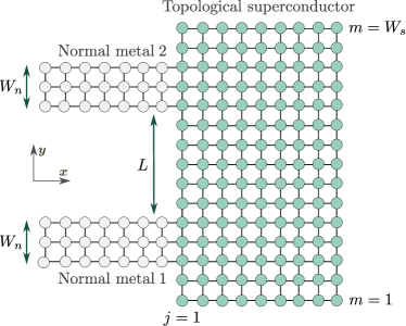
We numerically reproduce Eq. (23) and Eq. (24) using explicit models of TSs. We describe the present setup using a two-dimensional tight-binding model on a square lattice, as shown in Fig. 2. A lattice site is indicated by a vector , where and are unit vectors with length . The TS occupies and . The -th NM is placed on and , where and . We denote the width of the NM by and the distance between the first NM and the second NM by . In the direction, we apply an open boundary condition.
We discuss the topological superconductivity realized in superconducting topological insulator thin films [26, 37]. As will be discussed in detail later, the model we use can describe TSs belonging to both class D and class DIII by tuning the parameters [26, 37]. The model is given by the Bogoliubov–de Gennes Hamiltonian,
| (25) | ||||
where we assume that the low-energy physics consists only of Dirac surface states at the top and bottom layers of the topological insulator thin film. () is an annihilation operator of a Dirac electron at the top (bottom) layer with momentum and spin . The Pauli matrices and for denote the layer and spin degrees of freedom, respectively. The Hamiltonian describes the Dirac surface states. The second term , which is similar to the Wilson mass term [79, 80], opens gaps at the spurious Dirac points located at , while leaving the Dirac point at gapless. The coupling between the top and bottom Dirac surface states is denoted by . The chemical potential at the top (bottom) layer is given by (), where the potential difference between the top and bottom layers can be induced by an applied electric field along the out-of-plane direction [37]. We also consider the exchange potential along the axis, which can be induced by the intrinsic ferromagnetic ordering [81], magnetic doping [82], or magnetic proximity effects [83], where the exchange potential at the top (bottom) layer is represented by (). We assume that the extended -wave pair potential in the bulk provides a self-proximity effect on the Dirac surface states [34], where the effective pair potential acting on the Dirac surface states is denoted by . For the numerical calculations, we rewrite in a real space basis by applying a Fourier transformation: . The -th NM is described by
| (26) | ||||
where annihilates an electron at a site with spin , and represents the summation over the lattice sites in the -th NM. We describe the junction interface between the TS and the -th NM by
| (27) |
where we assume that the coupling is independent of the spins, while it depends on the leads and layers. In the following calculations, we fix the parameters as , , , , and . To highlight the robustness of our conclusion, we assume the irregular couplings at the interfaces: , satisfying . The scattering coefficients in Eq. (1) and Eq. (3) are numerically computed using recursive Green’s function techniques [84, 85].
III.1 Class D
First, we consider a TS belonging to class D, where we set the parameters as , , , , and . We assume the uniform chemical potential (i.e., ) and the simple -wave pair potential (i.e., ), for simplicity. Note that a very similar model was proposed in Ref. [26]; the pair potential in Ref. [26] has the layer dependence, while the exchange potential in our model has the layer dependence. For , as shown in detail in the Supplemental Material (SM) [86], the low-energy effective Hamiltonian for the superconducting segment is given by
| (28) | ||||
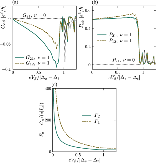
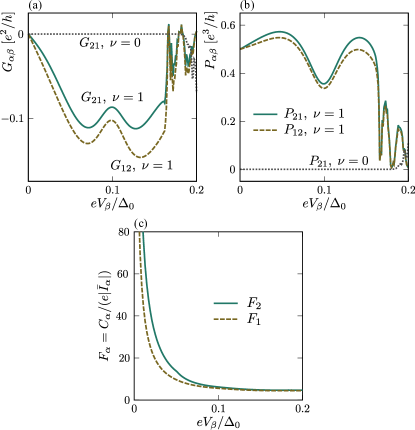
where are the three Pauli matrices. The effective Hamiltonian is equivalent to the Hamiltonian of a superconducting quantum anomalous Hall insulator [25]. According to Ref. [25], the Hamiltonian is characterized by a topological invariant, with a value of for , and for . The system with is topologically equivalent to the normal quantum anomalous Hall insulator, and hosts the residue of the normal chiral edge modes. The system with hosts single unpaired CMEMs moving in the direction from the first to the second NMs. The exact topological phase boundary is numerically computed in the SM [86]. In the following, we choose and to describe the topological phases with and , respectively. In Fig. 3(a) and Fig. 3(b), we show and as a function of the bias voltage, respectively. The solid lines show and with . The values of and for finite voltages can depend on the details of the parameters. Nevertheless, in perfect agreement with Eq. (23) and Eq. (24), we find and at zero bias voltage. The dashed lines show and with . Since the CMEM does not mediate inter-lead scatterings from the second to the first NMs, we obtain for bias voltages below the superconducting gap. The dotted lines show the results with . Both and are finite due to the presence of chiral edge modes. However, since these states are not unpaired CMEMs, we find even at zero bias voltage. This allows us to distinguish the unpaired CMEMs from other chiral edge modes. In Fig. 3(c), we show the noise-to-current ratio as a function of the bias voltage. For , we obtain independent of the bias voltage. For , we find the divergence of the noise-to-current ratio at zero bias voltage, which is a definitive signature of the CMEM.
III.2 Class DIII
Next, we consider a TS belonging to class DIII, where we set the parameters as , , , , and . To preserve time-reversal symmetry, we remove the exchange potential, . This model has been already proposed in Ref. [37]. For , as discussed in detail in the SM [86], we have two Fermi surfaces surrounding the point of the Brillouin zone. The Fermi surfaces are located at momenta satisfying with
| (29) | ||||
The extended -wave pair potential has zeros at satisfying
| (30) |
When the condition,
| (31) |
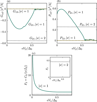
is satisfied, the quasiparticles on inner Fermi surface and that on the outer Fermi surface feel the pair potential with opposite signs, leading to the emergence of the topological superconductivity characterized by the topological index [30, 87]. In the following, we choose and to describe the phases with and , respectively, where the topological phase boundary is numerically computed in the SM [86]. In Fig. 4(a) and Fig. 4(b), we show and as a function of the bias voltage, respectively. The solid (dashed) lines denote and ( and ) with . Since the HMEM mediates the inter-lead scatterings in both directions, we find and , while at zero bias voltage. This result clearly agrees with Eq. (23) and Eq. (24). The dotted line shows the results for . Due to the absence of propagating edge modes, we find for bias voltages below the superconducting gap. In Fig. 4(c), we show the noise-to-current ratio with as a function of the bias voltage. In the presence of the HMEM, both and show the divergence at zero bias voltage. As already shown in Fig. 3(c), the CMEM causes the divergence in only one direction. Therefore, the proposed experiment enables a clear distinction between HMEMs and CMEMs.
IV Discussion and Summary
A recent experiment on the CoSi2/TiSi2 heterostructure [68] has observed an anomalous proximity effect [88, 89, 90, 91, 92], suggesting the realization of spin-triplet superconductivity in this system. Since the heterostructure exhibits strong Rashba-type spin-orbit coupling, the noncentrosymmetric ()-wave pairing with the dominant -wave component [93, 94, 95] is considered the most plausible pairing in the CoSi2/TiSi2 heterostructure [69]. However, the anomalous proximity effect can also be induced by spin-singlet superconductors with asymmetric spin-orbit coupling [96, 97, 98]. In the SM [86], we show that the noncentrosymmetric ()-wave superconductor exhibits the divergent noise-to-current ratio only when the -wave component is dominant (i.e., when the HMEMs exist). Therefore, the proposed experiment is useful for determining the pairing symmetry in this system.
Recently, the iron-based superconductor FeTe1-xSex has attracted much attention as a promising candidate for a higher-order TS hosting Majorana hinge states [70, 71, 72]. Theoretical studies have proposed the emergence of both helical Majorana hinge states [70] and chiral Majorana hinge states [71, 72]. Tunneling spectroscopy addressing the hinge of FeTe1-xSex has already been performed experimentally [73]. We hope that our proposal will inspire further experiments for the definitive verification of the Majorana hinge states in this compound.
In summary, we study the multi-terminal transport in systems consisting of the two NMs and the TS. We show analytically that the unpaired nature of the dispersing MEMs generally leads to the absence of time-averaged charge currents in the linear response limit, while the current fluctuation remains significant. We numerically reproduce the analytical predictions using the tight-binding models of the topological-insulator-based TSs. Since the current shot noise is more difficult to measure experimentally than the differential conductance, observing at zero bias voltage would be an efficient and practical first step in demonstrating the dispersing MEMs. Nevertheless, observing the divergence of the noise-to-current ratio provides more definitive evidence for the dispersing MEMs. Our theory suggests a promising way to unambiguously detect the dispersing MEMs in topological superconductors, such as CoSi2/TiSi2 heterostructures and iron-based superconductors FeTe1-xSex.
Acknowledgements.
We thank K. Hashimoto, J. Shiogai, T. Arakawa, M. Roppongi, and S. Liu for the fruitful discussions. S.I. is supported by a Grant-in-Aid for JSPS Fellows (JSPS KAKENHI Grant No. JP22KJ1507) and a Grant-in-Aid for Early-Career Scientists (JSPS KAKENHI Grant No. JP24K17010).References
- [1] N. Read and D. Green, Phys. Rev. B 61, 10267 (2000).
- [2] A. Y. Kitaev, Phys. Usp. 44, 131 (2001).
- [3] F. Wilczek, Nat. Phys. 5, 614-618 (2009).
- [4] M. Z. Hasan and C. L. Kane, Rev. Mod. Phys. 82, 3045 (2010).
- [5] X.-L. Qi and S.-C. Zhang, Rev. Mod. Phys. 83, 1057 (2011).
- [6] D. A. Ivanov, Phys. Rev. Lett. 86, 268 (2001).
- [7] A. Y. Kitaev, Ann. Phys. 303, 2-30 (2003).
- [8] C. Nayak, S. H. Simon, A. Stern, M. Freedman, and S. Das Sarma, Rev. Mod. Phys. 80, 1083(2008).
- [9] J. Alicea, Y. Oreg, G. Refael, F. v. Oppen, and M. P. A. Fisher, Nat. Phys. 7, 412-417(2011).
- [10] D. Aasen, M. Hell, R. V. Mishmash, A. Higginbotham, J. Danon, M. Leijnse, T. S. Jespersen, J. A. Folk, C. M. Marcus, K. Flensberg, and J. Alicea, Phys. Rev. X 6, 031016 (2016).
- [11] M. Sato, Y. Takahashi, and S. Fujimoto, Phys. Rev. Lett. 103, 020401 (2009).
- [12] J. D. Sau, R. M. Lutchyn, S. Tewari, and S. Das Sarma Phys. Rev. Lett. 104, 040502 (2010).
- [13] R. M. Lutchyn, J. D. Sau, and S. Das Sarma, Phys. Rev. Lett. 105, 077001 (2010).
- [14] Y. Oreg, G. Refael, and F. von Oppen, Phys. Rev. Lett. 105, 177002 (2010).
- [15] V. Mourik, K. Zuo, S. M. Frolov, S. R. Plissard, E. P. A. M. Bakkers, and L. P. Kouwenhoven, Science 336, 1003-1007 (2012).
- [16] M. Hell, M. Leijnse, and K. Flensberg, Phys. Rev. Lett. 118, 107701 (2017).
- [17] F. Pientka, A. Keselman, E. Berg, A. Yacoby, A. Stern, and B. I. Halperin, Phys. Rev. X 7, 021032 (2017).
- [18] A. Fornieri, A. M. Whiticar, F. Setiawan, E. Portolés, A. C. C. Drachmann, A. Keselman, S. Gronin, C. Thomas, T. Wang, R. Kallaher, G. C. Gardner, E. Berg, M. J. Manfra, A. Stern, C. M. Marcus, and F. Nichele, Nature 569, 89-92 (2019).
- [19] H. Ren, F. Pientka, S. Hart, A. T. Pierce, M. Kosowsky, L. Lunczer, R. Schlereth, B. Scharf, E. M. Hankiewicz, L. W. Molenkamp, B. I. Halperin, and A. Yacoby, Nature 569, 93-98 (2019).
- [20] T.-P. Choy, J. M. Edge, A. R. Akhmerov, and C. W. J. Beenakker, Phys. Rev. B 84, 195442 (2011).
- [21] S. Nadj-Perge, I. K. Drozdov, B. A. Bernevig, and A. Yazdani, Phys. Rev. B 88, 020407(R) (2013).
- [22] S. Nadj-Perge, I. K. Drozdov, J. Li, H. Chen, S. Jeon, J. Seo, A. H. MacDonald, B. A. Bernevig, and A. Yazdani, Science 346, 602-607 (2014).
- [23] G. C. Ménard, S. Guissart, C. Brun, R. T. Leriche, M. Trif, F. Debontridder, D. Demaille, D. Roditchev, P. Simon, and Tristan Cren, Nat. Commun. 8, 2040 (2017).
- [24] L. Fu and C. L. Kane, Phys. Rev. Lett. 100, 096407 (2008).
- [25] X.-L. Qi, T. L. Hughes, and S.-C. Zhang, Phys. Rev. B 82, 184516 (2010).
- [26] J. Wang, Q. Zhou, B. Lian, and S.-C. Zhang, Phys. Rev. B 92. 064520 (2015).
- [27] S. Sasaki, M. Kriener, K. Segawa, K. Yada, Y. Tanaka, M. Sato, and Y. Ando, Phys. Rev. Lett. 107, 217001 (2011).
- [28] T. H. Hsieh and L. Fu, Phys. Rev. Lett. 108, 107005 (2012).
- [29] A. Yamakage, K. Yada, M. Sato, and Y. Tanaka, Phys. Rev. B 85, 180509(R) (2012).
- [30] F. Zhang, C. L. Kane, and E. J. Mele, Phys. Rev. Lett. 111, 056402 (2013).
- [31] Z. Wang, P. Zhang, G. Xu, L. K. Zeng, H. Miao, X. Xu, T. Qian, H. Weng, P. Richard, A. V. Fedorov, H. Ding, Xi Dai, and Z. Fang Phys. Rev. B 92, 115119 (2015).
- [32] G. Xu, B. Lian, P. Tang, X.-L. Qi, and S.-C. Zhang, Phys. Rev. Lett. 117, 047001 (2016).
- [33] J-X. Yin, Z. Wu, J.-H.Wang, Z.-Y. Ye, J. Gong, X.-Y. Hou, L. Shan, A. Li, X.-J. Liang, X.-X.Wu, J. Li, C.-S. Ting, Z.-Q.Wang, J.-P. Hu, P.-H. Hor, H. Ding, and S. H. Pan, Nat. Phys. 11, 543–546 (2015).
- [34] P. Zhang, K. Yaji, T. Hashimoto, Y. Ota, T. Kondo, K. Okazaki, Z. Wang, J. Wen, G. D. Gu, H. Ding, Shik Shin, Science 360, 182–186 (2018).
- [35] D. Wang, L. Kong, P. Fan, H. Chen, S. Zhu, W. Liu, L. Cao, Y. Sun, S. Du, J. Schneeloch, R. Zhong, G. Gu, L. Fu, H. Ding, and H.-J. Gao, Science 362, 333–335 (2018).
- [36] T. Machida, Y. Sun, S. Pyon, S. Takeda, Y. Kohsaka, T. Hanaguri, T. Sasagawa, and T. Tamegai Nat. Mater. 18, 811–815 (2019).
- [37] R.-X. Zhang and S. Das Sarma, Phys. Rev. Lett. 126. 137001 (2021).
- [38] Microsoft Azure Quantum, Nature 638, 651–655 (2025).
- [39] L. J. Buchholtz and G. Zwicknagl, Phys. Rev. B 23, 5788 (1981).
- [40] C.-R. Hu, Phys. Rev. Lett. 72, 1526 (1994).
- [41] Y. Tanaka and S. Kashiwaya, Phys. Rev. Lett. 74, 3451 (1995).
- [42] K. Sengupta, I. Žutić, H.-J. Kwon, V. M. Yakovenko, and S. DasSarma, Phys. Rev. B 63, 144531 (2001).
- [43] Y. Asano, Y. Tanaka, and S. Kashiwaya, Phys. Rev. B 69, 134501 (2004).
- [44] K. T. Law, P. A. Lee, and T. K. Ng, Phys. Rev. Lett. 103, 237001 (2009).
- [45] G. Kells, D. Meidan, and P. W. Brouwer, Phys. Rev. B 86, 100503(R) (2012).
- [46] E. Prada, P. San-Jose, and R. Aguado, Phys. Rev. B 86, 180503(R) (2012).
- [47] C.-X. Liu, J. D. Sau, T. D. Stanescu, and S. Das Sarma Phys. Rev. B 96, 075161 (2017).
- [48] O. Dmytruk , D. Loss , and J. Klinovaja, Phys. Rev. B 102, 245431 (2020).
- [49] M. Kayyalha, D. Xiao, R. Zhang, J. Shin, J. Jiang, F. Wang, Y.-F. Zhao, R. Xiao, L. Zhang, K. M. Fijalkowski, P. Mandal, M. Winnerlein, C. Gould, Q. Li, L. W. Molenkamp, M. H. W. Chan, N. Samarth, C.-Z. Chang, Science 367, 64–67 (2020).
- [50] M. Valentini, F. Peñaranda, A. Hofmann, M. Brauns, R. Hauschild, P. Krogstrup, P. San-Jose, E. Prada, R. Aguado, and G. Katsaros Science 373, 82–88 (2021).
- [51] P. Yu, J. Chen, M. Gomanko, G. Badawy, E. P. A. M. Bakkers, K. Zuo, V. Mourik, and S. M. Frolov, Nat. Phys. 17, 482–488 (2021).
- [52] A. Uday, G. Lippertz, B. Bhujel, A. A. Taskin, Y. Ando, arXiv: 2411.14903 (2024).
- [53] C. W. J. Beenakker, P. Baireuther, Y. Herasymenko, I. Adagideli, L. Wang, and A. R. Akhmerov, Phys. Rev. Lett. 122, 146803 (2019).
- [54] C. J. Beenakker, A. Grabsch, and Y. Herasymenko, SciPost Phys. 6, 022 (2019).
- [55] I. Adagideli, F. Hassler, A. Grabsch, M. Pacholski, and C. W. J. Beenakker, SciPost Phys. 8, 013 (2020).
- [56] A. R. Akhmerov, J. Nilsson, and C. W. J. Beenakker, Phys. Rev. Lett. 102, 216404 (2009).
- [57] L. Fu and C. L. Kane, Phys. Rev. Lett. 102, 216403 (2009).
- [58] I. Serban, B. Béri, A. R. Akhmerov, and C. W. J. Beenakker, Phys. Rev. Lett. 104, 147001 (2010).
- [59] B. Béri, Phys. Rev. B 85, 140501(R) (2012).
- [60] N. V. Gnezdilov, B. van Heck, M. Diez, Jimmy A. Hutasoit, and C. W. J. Beenakker, Phys. Rev. B 92, 121406(R) (2015).
- [61] S. Ikegaya, Y. Asano, and D. Manske, Phys. Rev. Lett. 123, 207002 (2019).
- [62] G. Deutscher and D. Feinberg, Appl. Phys. Lett. 76, 487 (2000).
- [63] R.-J. Slager, L. Rademaker, J. Zaanen, and L. Balents, Phys. Rev. B 92, 085126 (2015).
- [64] W. A. Benalcazar, J. C. Y. Teo, and T. L. Hughes, Phys. Rev. B 89, 224503 (2014).
- [65] Z. Song, Z. Fang, and C. Fang, Phys. Rev. Lett. 119, 246402 (2017).
- [66] J. Langbehn, Y. Peng, L. Trifunovic, F. vonOppen, and P. W. Brouwer, Phys. Rev. Lett. 119, 246401 (2017).
- [67] E. Khalaf, Phys. Rev. B 97, 205136 (2018).
- [68] S.-P. Chiu, C. Tsuei, S.-S. Yeh, F.-C. Zhang, S. Kirchner, and J.-J. Lin, Sci. Adv. 7, eabg6569 (2021).
- [69] S.-P. Chiu, V. Mishra, Y. Li, F.-C. Zhang, S. Kirchner, and J.-J. Lin, Nanoscale 15, 9179 (2023).
- [70] R.-X. Zhang, W. S. Cole, and S. Das Sarma, Phys. Rev. Lett. 122 187001 (2019).
- [71] X. Wu, S. B. Chung, C. Liu, and E.-A. Kim, Phys. Rev. Research 3, 013066 (2021).
- [72] L.-H. Hu and R.-X. Zhang, Nat. Commun. 15, 2337 (2024).
- [73] M. J. Gray, J. Freudenstein, S. Y. F. Zhao, R. O’Connor, S. Jenkins, N. Kumar, M. Hoek, A. Kopec, S. Huh, T. Taniguchi, K. Watanabe, R. Zhong, C. Kim, G. D. Gu, and K. S. Burch, Nano Lett. 19, 4890(2019).
- [74] G. E. Blonder, M. Tinkham, and T. M. Klapwijk, Phys .Rev. B 25, 4515 (1982).
- [75] M. J. M. de Jong and C. W. J. Beenakker, Phys. Rev. B 49, 16070 (1994).
- [76] M. P. Anantram and S. Datta, Phys. Rev. B 53, 16390 (1996).
- [77] C. W. J. Beenakker, Rev. Mod. Phys. 87, 1037 (2015).
- [78] A. P. Schnyder, S. Ryu, A. Furusaki, and A. W. W. Ludwig, Phys. Rev. B 78, 195125 (2008).
- [79] K. G. Wilson, Phys. Rev. D 10. 2445 (1974).
- [80] Y.-F. Zhou, H. Jiang, X. C. Xie, and Q.-F. Sun, Phys. Rev. B 95. 245137 (2017).
- [81] N. Zaki, G. Gu, A. Tsvelik, C. Wu, and P.D. Johnson, Proc. Natl. Acad. Sci. U.S.A. 118, e2007241118 (2021).
- [82] Y. L. Chen, J.-H. Chu, J. G. Analytis, Z. K. Liu, K. Igarashi, H.-H. Kuo, X. L. Qi, S. K. Mo, R. G. Moore, D. H. Lu, M. Hashimoto, T. Sasagawa, S. C. Zhang, I. R. Fisher, Z. Hussain, and Z. X. Shen, Science 329, 659-662 (2010).
- [83] P. Wei, F. Katmis, B. A. Assaf, H. Steinberg, P. Jarillo-Herrero, D. Heiman, and J. S. Moodera, Phys. Rev. Lett. 110, 186807 (2013).
- [84] P. A. Lee and D. S. Fisher, Phys. Rev. Lett. 47, 882 (1981).
- [85] T. Ando, Phys. Rev. B 44, 8017 (1991).
- [86] Supplemental Material at XXX for the detailed discussion on the topological properties of the tight-binding Hamiltonian in Eq. (25). We also describe the divergence in the noise-to-current ratio of a noncentrosymmetric ()-wave superconductor.
- [87] X.-L. Qi, T. L. Hughes, and S.-C. Zhang, Phys. Rev. B 81, 134508 (2010).
- [88] Y. Tanaka and S. Kashiwaya, Phys. Rev. B 70, 012507 (2004).
- [89] Y. Tanaka, S. Kashiwaya, and T. Yokoyama, Phys. Rev. B 71, 094513 (2005).
- [90] Y. Asano, Y. Tanaka, A. A. Golubov, and S. Kashiwaya, Phys. Rev. Lett. 99, 067005 (2007).
- [91] S. Ikegaya, Y. Asano, and Y. Tanaka, Phys. Rev. B 91, 174511 (2015).
- [92] S. Ikegaya, S.-I. Suzuki, Y. Tanaka, and Y. Asano, Phys. Rev. B 94, 054512 (2016).
- [93] S. Fujimoto, J. Phys. Soc. Jpn. 76, 051008 (2007).
- [94] C. Iniotakis, N. Hayashi, Y. Sawa, T. Yokoyama, U. May, Y. Tanaka, and M. Sigrist, Phys. Rev. B 76, 012501 (2007).
- [95] M. Sato and S. Fujimoto, Phys. Rev. B 79, 094504 (2009).
- [96] S. Tamura and Y. Tanaka, Phys. Rev. B 99, 184501 (2019).
- [97] S. Ikegaya, J. Lee, A. P. Schnyder, and Y. Asano, Phys. Rev. B 104, L020502 (2021).
- [98] J. Lee, S. Ikegaya, and Y. Asano, arXiv:2501.17369 (2025).
Supplemental Material for
“Noise-to-current ratio divergence as a fingerprint of dispersing Majorana edge modes”
Leo Katayama1, Andreas P. Schnyder2, Yasuhiro Asano3, and Satoshi Ikegaya1,4
1Department of Applied Physics, Nagoya University, Nagoya 464-8603, Japan
2Max-Planck-Institut für Festkörperforschung, Heisenbergstrasse 1, D-70569 Stuttgart, Germany
3Department of Applied Physics, Hokkaido University, Sapporo 060-8628, Japan
4Institute for Advanced Research, Nagoya University, Nagoya 464-8601, Japan
March 5, 2025
V Topological Properties of Superconducting
Topological Insulator Thin-Films
In this section, we discuss the topological properties of the superconducting topological insulator thin-film [26, 37], which is described by the tight-binding Hamiltonian in Eq. (19) of the main text:
| (32) | ||||
where () is an annihilation operator of an electron at the top (bottom) layer with momentum and spin . The Pauli matrices and for denote the layer and spin degrees of freedom, respectively. The Hamiltonian describes the Dirac surface states. The second term opens the gaps at the spurious Dirac points at , while leaving the Dirac point at gapless. The coupling between the top and bottom Dirac surface states is denoted by . The chemical potential at the top (bottom) layer is given by (). The exchange potential at the top (bottom) layer is represented by (). The extended -wave pair potential acting on the Dirac surface states is denoted by .
V.1 class D
First, we focus on a topological superconductor (TS) belonging to class D, where we set the parameters as , for simplicity. By using a unitary operator,
| (33) | ||||
we deform the Hamiltonian as
| (34) | ||||
where are the three Pauli matrices. When , the normal bands described by pinch off from the Fermi level and do not affect the low-energy excitation, . Therefore, in this parameter regime, we obtain the effective Hamiltonian,
| (37) |
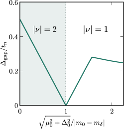
which is equivalent to Eq. (22) in the main text. The effective Hamiltonian is equivalent to the Hamiltonian of a superconducting quantum anomalous Hall insulator [25]. When and , the energy spectrum becomes gapless at , , and . Therefore, according to Ref. [25], the Hamiltonian is characterized by a topological invariant, with a value of for , and for . In Fig. 5, we show the superconducting gap size as a function of , where we fix . The superconducting gap size (i.e., the minimum positive energy eigenvalue) is obtained by diagonalizing numerically. The parameters are chosen as , , , . We confirm that the superconducting gap vanishes at . In the main text, we choose and to describe the topological phases with and , respectively.
V.2 class DIII
Next, we consider the TS belonging to class DIII, where we remove the exchange potential to preserve time-reversal symmetry (i.e., ). By diagonalizing , we obtain the energy eigenvalues of the normal state as,
| (38) | ||||
For , only brunch forms the Fermi surfaces. For , both and individually form a Fermi surface surrounding the point of the Brillouin zone. Specifically, the Fermi surfaces are located at momenta satisfying , where . The extend -wave pair potential has zeros at satisfying
| (39) |
When the condition,
| (40) |
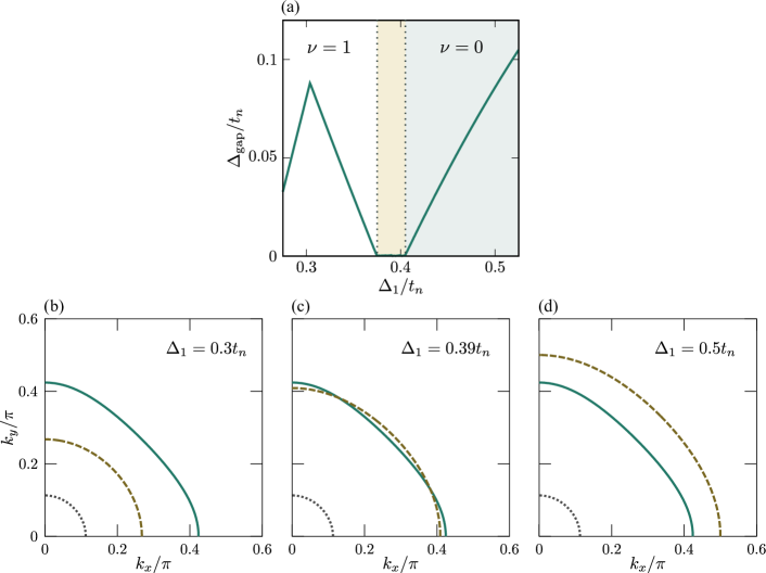
is satisfied, the inner Fermi surface and the outer Fermi surface feel the pair potential with opposite signs. This condition leads to the emergence of the topological superconductivity characterized by topological index [87, 30]. In Fig. 6(a), we show the superconducting gap size as a function of , where we choose , , , , , and . The superconducting gap size is obtained by diagonalizing numerically. We find that the superconducting gap vanishes around at . For this parameter region, we obtain the nodal superconducting states. In Fig. 6(c), we show the Fermi surfaces at , where the solid and dotted lines denote the Fermi surfaces of and , respectively. The dashed line represents the momenta where the pair potential vanishes, i.e., . The gap nodes appear at momenta where the solid and dashed lines intersect. For , we obtain the topologically nontrivial phase with , where the condition of is satisfied as shown in Fig. 6(b). For , we obtain the topologically trivial phase with as shown in Fig. 6(d). In the main text, we choose and to describe the phases with and , respectively.
VI Noncentrosymmetric Superconductors
In this section, we study the transport properties of a noncantrosymmetric ()-wave superconductor. We describe the present superconductor using a two-dimensional tight-binding model on a square lattice, as shown in Fig. 2 of the main text. The Bogoliubov–de Gennes (BdG) Hamiltonian reads [93, 94, 95],
| (41) | ||||
where is an annihilation operator of an electron with momentum and spin , is the nearest-neighbor hopping integral, represents the chemical potential. The strength of Rashba spin-orbit coupling is given by . The pair potential contains both a spin-singlet -wave component and a spin-triplet -wave component . Here we briefly discuss the topological properties of the noncentrosymmetric ()-wave superconductor. The positive energy eigen values of are given by
| (42) |
The superconducting gap vanishes at
| (43) |
where satisfies . For (), the BdG Hamiltonian can be deformed into the BdG Hamiltonian of a pure spin-singlet -wave (pure spin-triplet helical -wave) superconductor without any gap closing by decreasing and () adiabatically. The helical -wave superconductor is a time-reversal invariant topological superconductor characterized by a topological invariant of . Thus, for , the noncentrosymmetric ()-wave superconductor is topologically equivalent to the helical -wave superconductor and hosts the helical Majorana edge mode (HMEM) [93, 94, 95]. For the numerical calculations, we rewrite in a real space basis by applying a Fourier transformation: . The -th normal metal is described by
| (44) |
where annihilates an electron at a site with spin , and represents the summation over the lattice sites in the -th normal metal. We describe the junction interface between the noncentrosymmetric ()-wave superconductor and the -th normal metal by
| (45) |
where we assume that the coupling is independent of the spins, while it depends on the leads. In the following calculations, we fix the parameters as , , , , , , and . To describe the topologically nontrivial phase with and the topologically trivial phase with , we choose and , respectively. In Fig. 7(a) and Fig. 7(b), we show and as a function of the bias voltage, respectively. The dotted line shows the results for . Due to the absence of propagating edge modes, we find for bias voltages below the superconducting gap. The solid (dashed) lines denote and ( and ) with . Since the HMEM mediates the inter-lead scatterings in both directions, we find and , while at zero bias voltage. Therefore, as demonstrated in Fig. 7(c), we obtain the divergence of the noise-to-current ratio at zero bias voltage. The divergent noise-to-current ratio is a definitive signature of the dominant -wave pairing that is responsible for the appearance of the HMEM.