Low crosstalk modular flip-chip architecture for coupled superconducting qubits
Abstract
We present a flip-chip architecture for an array of coupled superconducting qubits, in which circuit components reside inside individual microwave enclosures. In contrast to other flip-chip approaches, the qubit chips in our architecture are electrically floating, which guarantees a simple, fully modular assembly of capacitively coupled circuit components such as qubit, control, and coupling structures, as well as reduced crosstalk between the components. We validate the concept with a chain of three nearest neighbor coupled generalized flux qubits in which the center qubit acts as a frequency-tunable coupler. Using this coupler, we demonstrate a transverse coupling on/off , between resonant qubits and isolation between the qubit .
Circuit quantum electrodynamics [1] — using superconducting qubits, resonators and waveguides as building blocks — is one of the leading platforms for quantum hardware development. Following an approach similar to the semiconductor industry, the on-chip integration of an increasing number of such components is, in principle, a matter of sophisticated engineering and it has led to the realization of impressively complex quantum processors [2, 3, 4, 5, 6, 7, 8]. However, as quantum processors grow in size and complexity, new physical phenomena emerge, such as correlated quasiparticle and phonon bursts [9, 10], charge offsets [11] and two-level-system reconfigurations due to ionizing radiation [12, 13]. Moreover, microwave crosstalk emerges as one of the main limitations in some of the most sophisticated architectures [8]. Last, but not least, it becomes increasingly likely that frequency crowding or a single defective component limits the performance of an entire chip. In view of these challenges, it is essential for scale-up strategies to minimize microwave and mechanical (i.e. phonon) crosstalk and maximize modularity.
On-chip strategies to scale-up quantum processors include from a technological perspective relatively involved techniques such as air-bridges [14], spring-loaded pogo pins [15] or deep silicon vias [16]. While these monolithic devices can achieve impressive microwave performance in terms of isolation and spurious mode suppression, they are susceptible to correlated phonon bursts and lack modularity due to cold-welded connections between layers. A complementary approach is to assemble a processor from chip-level building blocks, allowing for individual component fabrication, as well as flexible and reconfigurable arrangements. Several promising techniques are currently being pursued [17, 18, 19, 20], including flip-chip [21, 22] and chiplet [23, 24, 25] architectures.
Here we present an alternative modular approach, where we combine several features of 2D and 3D architectures to form an array of coupled, but crosstalk-resilient superconducting qubits. Our goal is to facilitate a highly modular assembly, with microwave-isolated sub-components insensitive to correlated errors caused by the propagation of phonon waves. The key feature in our design is the separation of the qubits on dedicated, electrically floating chips within individual microwave enclosures. To validate the architecture, we implemented a device consisting of three enclosures, each hosting a generalized flux qubit, inductively coupled to a dedicated readout mode (QR system) similar to Ref. [26]. We use the central qubit as a flux-tunable coupler and demonstrate tunable two-qubit interactions. This concept can be extended by adding microwave enclosures, both in-plane and out-of-plane, to increase the number of adjacent qubits.
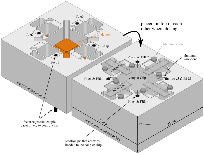
The three enclosures of our prototype, each hosting a QR system on a dedicated chip, are shown in Fig. 1a. They have dimensions of , pushing the enclosures lowest frequency eigenmodes above 16 GHz. The 6.5 mm spacing between neighboring qubits facilitates their assembly without the need for sophisticated packaging tools and strongly reduces crosstalk. In the outer enclosures on the left and right (e1 & e3 respectively, see Fig. 1b) we mount an upside-down flipped qubit chip on top of a control chip, while the middle enclosure (e2) contains only a single coupler chip. The qubit chip dimensions () exceed the size of their enclosures, so that they overlap with the adjacent enclosures. We attach the top qubit chips with a small amount of vacuum grease to pedestals inside the enclosures. We fix the bottom chips with titanium or copper screws to the sample box and wire bond to the coaxial ports. The pedestals define the m gap between the top and bottom chips, avoiding cold-welded bump bonds or on-chip spacers. The qubit chips contain a QR systems, as described in Ref. [26], to which we add capacitive extenders that reach into the adjacent enclosures (see Fig. 1b,c). The pads at the end of the extenders and in the center of the chips are used for capacitive coupling across the gap between the chips, which is discussed in more detail in App. A. We chose a skeletal pattern for the pads to avoid flux trapping. The coupler chip in e2 also houses a QR system connected via capacitive extenders to pads (see Fig. 1d), aligned with the corresponding neighboring qubits’ coupling pads. Details of the fabrication can be found in App. B.
The control chips below each qubit chip in e1 and e3 accommodate a bond pad, capacitively coupled to a band-pass filter, which is connected to a capacitive pad in the center of the qubit chip (see Fig. 1e). The band-pass filter reduces Purcell decay [29, 30], and enables the coupling of the readout mode to the coaxial input port (see App. A). The control structures for the coupler, which consist of a fast flux bias line (FBL) and a readout line as shown in Fig. 1d, are on the same chip. The FBL on the center coupler chip is wire-bonded to a coaxial cable, which is equipped with a 300 MHz low-pass filter.
The picture in Fig. 1f shows an open sample box made of copper and it provides an overview of the entire assembly of five chips thermally anchored to the base plate of a dilution cryostat. We show an equivalent circuit diagram of the assembly in Fig. 1g. Note that the three individual enclosures are defined by the lid, which is not visible in the picture. The simplified schematics of the microwave readout and control lines is also shown in Fig. 1f. We perform individual qubit readout by probing the readout resonators on the qubit chips in reflection. We use dimer Josephson junction array parametric amplifiers (DJJAAs) [27] for the readout of the two qubits in e1 & e3. Qubit control pulses are also send through the readout lines. Simultaneous readout and single qubit -pulse calibration measurement are shown in App. C.
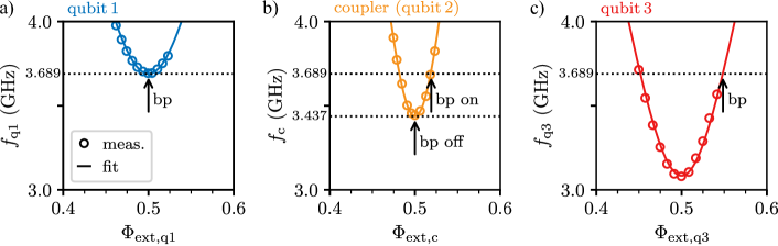
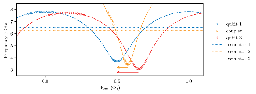
We show the measured two-tone spectroscopy for the qubits and coupler close to their half-flux points (i.e. the magnetic flux sweet spots) in Fig. 2. Their frequencies can be tuned independently via the three magnetic field coils, after calibrating the static magnetic field crosstalks. To operate the device, we define the idle points to be the sweet spots of qubit 1 and coupler, which are at GHz and GHz, respectively. Exploiting the fact that the qubits are isolated in distant enclosures, we chose to operate qubit 1 and 3 on resonance. To turn on coupling between qubit 1 and 3, we play fast flux pulses on the FBL to tune the coupler closer to the qubit 1 and 3 bias points.
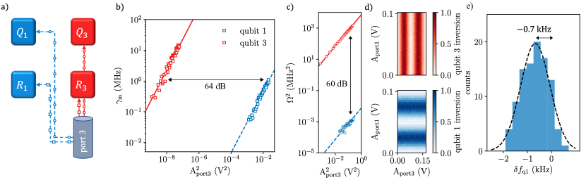
In view of the fact that we operate the qubits on resonance, it is paramount to know the isolation and crosstalk between the enclosures when the coupling is turned off. Fig. 3a illustrates schematically the crosstalk present in our system. To identify the port-to-resonator isolation, we drive resonator 1 ( GHz) and resonator 3 ( GHz) through the readout port of e3. We measure readout-induced dephasing for both qubits via Ramsey interferometry vs. drive power and drive frequency and fit it to a dispersive model [31], detailed in App. D. We extract the isolation between enclosures from the ratio of power transmission coefficients. Fitting the measured data shown in Fig. 3, we obtain an isolation of dB.
To test qubit control crosstalk we drive via port 3 and measure Rabi oscillations vs. drive amplitude on both qubits for a s long pulse. We fit the linear dependence of the measured Rabi frequencies with applied drive amplitude, as shown in Fig. 3c. Following references [20] and [32], we extract a port-to-qubit crosstalk, also known as qubit drive selectivity, of
| (1) |
which allows to drive simultaneous Rabi oscillations of qubit 1 and qubit 3 on resonance () with less than 1‰ crosstalk error.
We quantify the longitudinal interaction between qubits 1 and 3 by measuring Ramsey fringes on qubit 1, with and without playing a -pulse on qubit 3. The measured shifts in qubit 1 frequencies, , are summarized in Fig. 3d. The resulting zz-crosstalk is described by a Gaussian distribution with an average kHz and standard deviation kHz.
Compared to state-of-the-art conventional flip-chip architectures based on coplanar waveguide architectures [32], the isolation presented here is several orders of magnitude larger. Compared to similar architectures based on 3D-integrated floating chips in enclosures [20], the isolation is at least comparable or one order of magnitude larger on average. This proves the effective screening of microwave signals across the enclosures, even while capacitive extenders between the enclosures are present and while the qubits are operated on resonance.
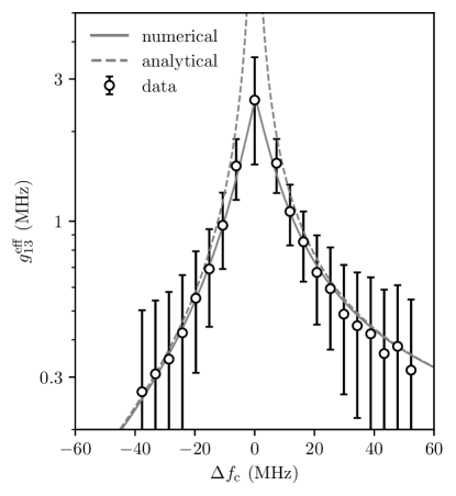
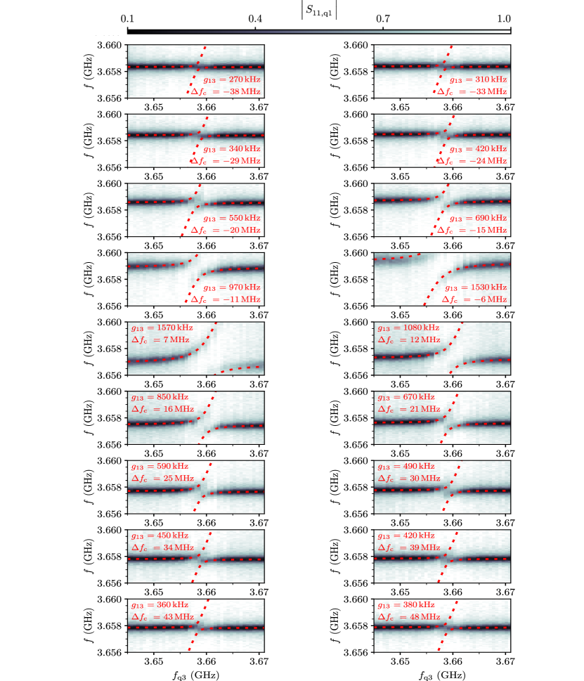
The effective transverse coupling strength between qubit 1 and 3 can be tuned by adapting the coupler detuning . To illustrate this, we show the measured in Fig. 4 which are obtained from two-tone spectroscopic measurements of avoided level splitting between qubits 1 and 3 for different coupler detunings (cf. App. E). By applying a Schrieffer-Wolff transformation (SWT) to the coupled three-qubit array, we obtain an effective two-qubit model [33, 34]. The SWT can be calculated numerically without approximation as explained in Ref. [33], and analytically using second-order perturbation, as detailed in App. F. The continuous and dashed lines in Fig. 4 show fits of the SWT model to the measured using two parameters: the effective qubit-coupler fF and direct qubit-qubit aF coupling capacitances, which are given by the combination of capacitive extenders and shunting capacitances via ground (cf. Fig. 1g). The individual qubit and coupler parameters are obtained from separate fits of their flux-dependent spectra [26] and summarized in App. G. As expected, perturbation theory fails to predict the level splitting close to resonance, whereas the numerical results capture the tunability of the effective qubit-qubit coupling correctly.
The coupling strength MHz is maximal on resonance, confirming the measured qubit population swap frequency , as detailed in App. H. At the coupler sweet spot, which corresponds to a detuning of MHz, we measure a residual kHz, corresponding to an ON/OFF ratio of 50 (see App. E, Fig. A6). In future experiments, the ON/OFF ratio can be optimized by designing the coupling capacitors and in such a way that the direct charge interaction between qubit 1 and 3, represented by a parasitic , cancels with the one mediated by the coupler, similarly to Ref. [35].
In summary, we have demonstrated a linear array of three coupled flux qubits, each on a dedicated chip in a separate microwave enclosure, which ensures low microwave crosstalk between the outermost enclosures, below -60 dB. We leverage this isolation and operate the qubits on resonance, using the center qubit as flux-tunable coupler. As a result, the architecture provides strong isolation while offering tunable coupling at the same time. In addition, the system is fully modular and allows for the substitution and reassembly of individual circuit parts.
In the future, this architecture can be used to implement two-qubit gates on resonant qubits by using the coupler off-resonantly [36, 37, 38, 35, 39] or to investigate novel gate schemes including the coupler degree of freedom. The one qubit one enclosure concept presented here is directly scalable in two dimensions (see App. I) and could potentially be miniaturized using micromachining techniques [40, 41, 42].
Acknowledgements
We are grateful to L. Radtke and S. Diewald for technical assistance. This project was financed by the European Commission via project FET-Open AVaQus, GA 899561. M.S., P.P., N.G. and T.R. acknowledge partial funding from the German Ministry of Education and Research (BMBF) within the project GEQCOS (FKZ: 13N15683). N.Z. acknowledges funding from the Deutsche Forschungsgemeinschaft (DFG – German Research Foundation) under project number 450396347 (GeHoldeQED). G.J. acknowledges support from the “la Caixa” Foundation (ID 100010434) via fellowship code LCF/BQ/DR22/11950032. M.P. acknowledges funding from European Union NextGenerationEU/PRTR project Consolidación Investigadora CNS2022-136025. Facilities use was supported by the KIT Nanostructure Service Laboratory. We acknowledge the measurement software framework qKit.
References
- Blais et al. [2021] A. Blais, A. L. Grimsmo, S. M. Girvin, and A. Wallraff, Circuit quantum electrodynamics, Rev. Mod. Phys. 93, 025005 (2021).
- Arute et al. [2019] F. Arute, K. Arya, R. Babbush, D. Bacon, J. C. Bardin, R. Barends, R. Biswas, S. Boixo, F. G. S. L. Brandao, D. A. Buell, B. Burkett, Y. Chen, Z. Chen, B. Chiaro, R. Collins, W. Courtney, A. Dunsworth, E. Farhi, B. Foxen, A. Fowler, C. Gidney, M. Giustina, R. Graff, K. Guerin, S. Habegger, M. P. Harrigan, M. J. Hartmann, A. Ho, M. Hoffmann, T. Huang, T. S. Humble, S. V. Isakov, E. Jeffrey, Z. Jiang, D. Kafri, K. Kechedzhi, J. Kelly, P. V. Klimov, S. Knysh, A. Korotkov, F. Kostritsa, D. Landhuis, M. Lindmark, E. Lucero, D. Lyakh, S. Mandrà, J. R. McClean, M. McEwen, A. Megrant, X. Mi, K. Michielsen, M. Mohseni, J. Mutus, O. Naaman, M. Neeley, C. Neill, M. Y. Niu, E. Ostby, A. Petukhov, J. C. Platt, C. Quintana, E. G. Rieffel, P. Roushan, N. C. Rubin, D. Sank, K. J. Satzinger, V. Smelyanskiy, K. J. Sung, M. D. Trevithick, A. Vainsencher, B. Villalonga, T. White, Z. J. Yao, P. Yeh, A. Zalcman, H. Neven, and J. M. Martinis, Quantum supremacy using a programmable superconducting processor, Nature 574, 505 (2019).
- Wu et al. [2021] Y. Wu, W.-S. Bao, S. Cao, F. Chen, M.-C. Chen, X. Chen, T.-H. Chung, H. Deng, Y. Du, D. Fan, M. Gong, C. Guo, C. Guo, S. Guo, L. Han, L. Hong, H.-L. Huang, Y.-H. Huo, L. Li, N. Li, S. Li, Y. Li, F. Liang, C. Lin, J. Lin, H. Qian, D. Qiao, H. Rong, H. Su, L. Sun, L. Wang, S. Wang, D. Wu, Y. Xu, K. Yan, W. Yang, Y. Yang, Y. Ye, J. Yin, C. Ying, J. Yu, C. Zha, C. Zhang, H. Zhang, K. Zhang, Y. Zhang, H. Zhao, Y. Zhao, L. Zhou, Q. Zhu, C.-Y. Lu, C.-Z. Peng, X. Zhu, and J.-W. Pan, Strong quantum computational advantage using a superconducting quantum processor, Phys. Rev. Lett. 127, 180501 (2021).
- Krinner et al. [2022] S. Krinner, N. Lacroix, A. Remm, A. Di Paolo, E. Genois, C. Leroux, C. Hellings, S. Lazar, F. Swiadek, J. Herrmann, G. J. Norris, C. K. Andersen, M. Müller, A. Blais, C. Eichler, and A. Wallraff, Realizing repeated quantum error correction in a distance-three surface code, Nature 605, 669 (2022).
- Marques et al. [2022] J. F. Marques, B. M. Varbanov, M. S. Moreira, H. Ali, N. Muthusubramanian, C. Zachariadis, F. Battistel, M. Beekman, N. Haider, W. Vlothuizen, A. Bruno, B. M. Terhal, and L. DiCarlo, Logical-qubit operations in an error-detecting surface code, Nat. Phys. 18, 80 (2022).
- AI [2023] G. Q. AI, Suppressing quantum errors by scaling a surface code logical qubit, Nature 614, 676 (2023), [Online; accessed 6. Sep. 2024].
- Kim et al. [2023] Y. Kim, C. J. Wood, T. J. Yoder, S. T. Merkel, J. M. Gambetta, K. Temme, and A. Kandala, Scalable error mitigation for noisy quantum circuits produces competitive expectation values, Nat. Phys. 19, 752 (2023).
- Google Quantum AI and Collaborators [2024] Google Quantum AI and Collaborators, Quantum error correction below the surface code threshold, Nature 10.1038/s41586-024-08449-y (2024).
- Cardani et al. [2021] L. Cardani, F. Valenti, N. Casali, G. Catelani, T. Charpentier, M. Clemenza, I. Colantoni, A. Cruciani, G. D’Imperio, L. Gironi, L. Grünhaupt, D. Gusenkova, F. Henriques, M. Lagoin, M. Martinez, G. Pettinari, C. Rusconi, O. Sander, C. Tomei, A. V. Ustinov, M. Weber, W. Wernsdorfer, M. Vignati, S. Pirro, and I. M. Pop, Reducing the impact of radioactivity on quantum circuits in a deep-underground facility, Nat. Commun. 12, 1 (2021).
- McEwen et al. [2021] M. McEwen, L. Faoro, K. Arya, A. Dunsworth, T. Huang, S. Kim, B. Burkett, A. Fowler, F. Arute, J. C. Bardin, A. Bengtsson, A. Bilmes, B. B. Buckley, N. Bushnell, Z. Chen, R. Collins, S. Demura, A. R. Derk, C. Erickson, M. Giustina, S. D. Harrington, S. Hong, E. Jeffrey, J. Kelly, P. V. Klimov, F. Kostritsa, P. Laptev, A. Locharla, X. Mi, K. C. Miao, S. Montazeri, J. Mutus, O. Naaman, M. Neeley, C. Neill, A. Opremcak, C. Quintana, N. Redd, P. Roushan, D. Sank, K. J. Satzinger, V. Shvarts, T. White, Z. J. Yao, P. Yeh, J. Yoo, Y. Chen, V. Smelyanskiy, J. M. Martinis, H. Neven, A. Megrant, L. Ioffe, and R. Barends, Resolving catastrophic error bursts from cosmic rays in large arrays of superconducting qubits, Nature Physics 18, 107 (2021).
- Wilen et al. [2021] C. D. Wilen, S. Abdullah, N. A. Kurinsky, C. Stanford, L. Cardani, G. D’Imperio, C. Tomei, L. Faoro, L. B. Ioffe, C. H. Liu, A. Opremcak, B. G. Christensen, J. L. DuBois, and R. McDermott, Correlated charge noise and relaxation errors in superconducting qubits, Nature 594, 369 (2021).
- Thorbeck et al. [2023] T. Thorbeck, A. Eddins, I. Lauer, D. T. McClure, and M. Carroll, Two-Level-System Dynamics in a Superconducting Qubit Due to Background Ionizing Radiation, PRX Quantum 4, 020356 (2023).
- Yelton et al. [2024] E. Yelton, C. P. Larson, V. Iaia, K. Dodge, G. La Magna, P. G. Baity, I. V. Pechenezhskiy, R. McDermott, N. A. Kurinsky, G. Catelani, and B. L. T. Plourde, Modeling phonon-mediated quasiparticle poisoning in superconducting qubit arrays, Phys. Rev. B 110, 024519 (2024).
- Janzen et al. [2022] N. Janzen, M. Kononenko, S. Ren, and A. Lupascu, Aluminum air bridges for superconducting quantum devices realized using a single-step electron-beam lithography process, Applied Physics Letters 121, 094001 (2022), https://pubs.aip.org/aip/apl/article-pdf/doi/10.1063/5.0103165/16640448/094001_1_online.pdf .
- Bronn et al. [2018] N. T. Bronn, V. P. Adiga, S. B. Olivadese, X. Wu, J. M. Chow, and D. P. Pappas, High coherence plane breaking packaging for superconducting qubits, Quantum Science and Technology 3, 024007 (2018).
- Mallek et al. [2021] J. L. Mallek, D. R. W. Yost, D. Rosenberg, J. L. Yoder, G. Calusine, M. T. Cook, R. Das, A. L. Day, E. B. Golden, D. K. Kim, J. Knecht, B. M. Niedzielski, M. Schwartz, A. Sevi, C. Stull, W. Woods, A. J. Kerman, and W. D. Oliver, Fabrication of superconducting through-silicon vias (2021).
- Mollenhauer et al. [2024] M. Mollenhauer, A. Irfan, X. Cao, S. Mandal, and W. Pfaff, A high-efficiency plug-and-play superconducting qubit network (2024), arXiv:2407.16743 [quant-ph] .
- Chou et al. [2024] K. S. Chou, T. Shemma, H. McCarrick, T.-C. Chien, J. D. Teoh, P. Winkel, A. Anderson, J. Chen, J. C. Curtis, S. J. de Graaf, J. W. O. Garmon, B. Gudlewski, W. D. Kalfus, T. Keen, N. Khedkar, C. U. Lei, G. Liu, P. Lu, Y. Lu, A. Maiti, L. Mastalli-Kelly, N. Mehta, S. O. Mundhada, A. Narla, T. Noh, T. Tsunoda, S. H. Xue, J. O. Yuan, L. Frunzio, J. Aumentado, S. Puri, S. M. Girvin, S. H. Moseley, and R. J. Schoelkopf, A superconducting dual-rail cavity qubit with erasure-detected logical measurements, Nature Physics 10.1038/s41567-024-02539-4 (2024).
- Copetudo et al. [2024] A. Copetudo, C. Y. Fontaine, F. Valadares, and Y. Y. Gao, Shaping photons: Quantum information processing with bosonic cQED, Appl. Phys. Lett. 124, 080502 (2024).
- Spring et al. [2022a] P. A. Spring, S. Cao, T. Tsunoda, G. Campanaro, S. Fasciati, J. Wills, M. Bakr, V. Chidambaram, B. Shteynas, L. Carpenter, P. Gow, J. Gates, B. Vlastakis, and P. J. Leek, High coherence and low cross-talk in a tileable 3d integrated superconducting circuit architecture, Science Advances 8, eabl6698 (2022a), https://www.science.org/doi/pdf/10.1126/sciadv.abl6698 .
- Kosen et al. [2022] S. Kosen, H.-X. Li, M. Rommel, D. Shiri, C. Warren, L. Grönberg, J. Salonen, T. Abad, J. Biznárová, M. Caputo, L. Chen, K. Grigoras, G. Johansson, A. F. Kockum, C. Križan, D. P. Lozano, G. J. Norris, A. Osman, J. Fernández-Pendás, A. Ronzani, A. F. Roudsari, S. Simbierowicz, G. Tancredi, A. Wallraff, C. Eichler, J. Govenius, and J. Bylander, Building blocks of a flip-chip integrated superconducting quantum processor, Quantum Science and Technology 7, 035018 (2022).
- Conner et al. [2021] C. R. Conner, A. Bienfait, H.-S. Chang, M.-H. Chou, . Dumur, J. Grebel, G. A. Peairs, R. G. Povey, H. Yan, Y. P. Zhong, and A. N. Cleland, Superconducting qubits in a flip-chip architecture, Applied Physics Letters 118, 10.1063/5.0050173 (2021).
- Field et al. [2024] M. Field, A. Q. Chen, B. Scharmann, E. A. Sete, F. Oruc, K. Vu, V. Kosenko, J. Y. Mutus, S. Poletto, and A. Bestwick, Modular superconducting-qubit architecture with a multichip tunable coupler, Phys. Rev. Appl. 21, 054063 (2024).
- Bild et al. [2023] M. Bild, M. Fadel, Y. Yang, U. von Lüpke, P. Martin, A. Bruno, and Y. Chu, Schrödinger cat states of a 16-microgram mechanical oscillator, Science 380, 274 (2023).
- Yost et al. [2020] D. R. W. Yost, M. E. Schwartz, J. Mallek, D. Rosenberg, C. Stull, J. L. Yoder, G. Calusine, M. Cook, R. Das, A. L. Day, E. B. Golden, D. K. Kim, A. Melville, B. M. Niedzielski, W. Woods, A. J. Kerman, and W. D. Oliver, Solid-state qubits integrated with superconducting through-silicon vias, npj Quantum Information 6, 10.1038/s41534-020-00289-8 (2020).
- Geisert et al. [2024] S. Geisert, S. Ihssen, P. Winkel, M. Spiecker, M. Fechant, P. Paluch, N. Gosling, N. Zapata, S. Günzler, D. Rieger, D. Bénâtre, T. Reisinger, W. Wernsdorfer, and I. M. Pop, Pure kinetic inductance coupling for cQED with flux qubits, Appl. Phys. Lett. 125, 064002 (2024).
- Winkel et al. [2020] P. Winkel, I. Takmakov, D. Rieger, L. Planat, W. Hasch-Guichard, L. Grünhaupt, N. Maleeva, F. Foroughi, F. Henriques, K. Borisov, J. Ferrero, A. V. Ustinov, W. Wernsdorfer, N. Roch, and I. M. Pop, Nondegenerate parametric amplifiers based on dispersion-engineered josephson-junction arrays, Phys. Rev. Appl. 13, 024015 (2020).
- [28] Magnetic shielding, https://www.quantum-machines.co/products/qcage/, online; accessed 15-July-2024.
- Reed et al. [2010] M. D. Reed, B. R. Johnson, A. A. Houck, L. DiCarlo, J. M. Chow, D. I. Schuster, L. Frunzio, and R. J. Schoelkopf, Fast reset and suppressing spontaneous emission of a superconducting qubit, Appl. Phys. Lett. 96, 203110 (2010).
- Sete et al. [2015] E. A. Sete, J. M. Martinis, and A. N. Korotkov, Quantum theory of a bandpass purcell filter for qubit readout, Phys. Rev. A 92, 012325 (2015).
- Gambetta et al. [2006] J. Gambetta, A. Blais, D. I. Schuster, A. Wallraff, L. Frunzio, J. Majer, M. H. Devoret, S. M. Girvin, and R. J. Schoelkopf, Qubit-photon interactions in a cavity: Measurement-induced dephasing and number splitting, Phys. Rev. A 74, 042318 (2006).
- Kosen et al. [2024] S. Kosen, H.-X. Li, M. Rommel, R. Rehammar, M. Caputo, L. Grönberg, J. Fernández-Pendás, A. F. Kockum, J. Biznárová, L. Chen, C. Križan, A. Nylander, A. Osman, A. F. Roudsari, D. Shiri, G. Tancredi, J. Govenius, and J. Bylander, Signal crosstalk in a flip-chip quantum processor, PRX Quantum 5, 030350 (2024).
- Hita-Pérez et al. [2021] M. Hita-Pérez, G. Jaumà, M. Pino, and J. J. García-Ripoll, Three-Josephson junctions flux qubit couplings, Appl. Phys. Lett. 119, 222601 (2021).
- Consani and Warburton [2020] G. Consani and P. A. Warburton, Effective Hamiltonians for interacting superconducting qubits: local basis reduction and the Schrieffer–Wolff transformation, New J. Phys. 22, 053040 (2020).
- Sung et al. [2021] Y. Sung, L. Ding, J. Braumüller, A. Vepsäläinen, B. Kannan, M. Kjaergaard, A. Greene, G. O. Samach, C. McNally, D. Kim, A. Melville, B. M. Niedzielski, M. E. Schwartz, J. L. Yoder, T. P. Orlando, S. Gustavsson, and W. D. Oliver, Realization of High-Fidelity CZ and -Free iSWAP Gates with a Tunable Coupler, Phys. Rev. X 11, 021058 (2021).
- Chen et al. [2014] Y. Chen, C. Neill, P. Roushan, N. Leung, M. Fang, R. Barends, J. Kelly, B. Campbell, Z. Chen, B. Chiaro, A. Dunsworth, E. Jeffrey, A. Megrant, J. Y. Mutus, P. J. J. O’Malley, C. M. Quintana, D. Sank, A. Vainsencher, J. Wenner, T. C. White, M. R. Geller, A. N. Cleland, and J. M. Martinis, Qubit Architecture with High Coherence and Fast Tunable Coupling, Phys. Rev. Lett. 113, 220502 (2014).
- McKay et al. [2016] D. C. McKay, S. Filipp, A. Mezzacapo, E. Magesan, J. M. Chow, and J. M. Gambetta, Universal Gate for Fixed-Frequency Qubits via a Tunable Bus, Phys. Rev. Appl. 6, 064007 (2016).
- Weber et al. [2017] S. J. Weber, G. O. Samach, D. Hover, S. Gustavsson, D. K. Kim, A. Melville, D. Rosenberg, A. P. Sears, F. Yan, J. L. Yoder, W. D. Oliver, and A. J. Kerman, Coherent Coupled Qubits for Quantum Annealing, Phys. Rev. Appl. 8, 014004 (2017).
- Moskalenko et al. [2022] I. N. Moskalenko, I. A. Simakov, N. N. Abramov, A. A. Grigorev, D. O. Moskalev, A. A. Pishchimova, N. S. Smirnov, E. V. Zikiy, I. A. Rodionov, and I. S. Besedin, High fidelity two-qubit gates on fluxoniums using a tunable coupler, npj Quantum Inf. 8, 1 (2022).
- Brecht et al. [2017] T. Brecht, Y. Chu, C. Axline, W. Pfaff, J. Z. Blumoff, K. Chou, L. Krayzman, L. Frunzio, and R. J. Schoelkopf, Micromachined Integrated Quantum Circuit Containing a Superconducting Qubit, Phys. Rev. Appl. 7, 044018 (2017).
- Rosenberg et al. [2020] D. Rosenberg, S. J. Weber, D. Conway, D.-R. W. Yost, J. Mallek, and G. Calusine, Solid-State Qubits: 3D Integration and Packaging, IEEE Microwave Mag. 21, 72 (2020).
- Spring et al. [2022b] P. A. Spring, S. Cao, T. Tsunoda, G. Campanaro, S. Fasciati, J. Wills, M. Bakr, V. Chidambaram, B. Shteynas, L. Carpenter, P. Gow, J. Gates, B. Vlastakis, and P. J. Leek, High coherence and low cross-talk in a tileable 3D integrated superconducting circuit architecture, Sci. Adv. 8, 10.1126/sciadv.abl6698 (2022b).
- Bravyi et al. [2011] S. Bravyi, D. P. DiVincenzo, and D. Loss, Schrieffer–Wolff transformation for quantum many-body systems, Ann. Phys. 326, 2793 (2011).
- Hita-Pérez et al. [2022] M. Hita-Pérez, G. Jaumà, M. Pino, and J. J. García-Ripoll, Ultrastrong Capacitive Coupling of Flux Qubits, Phys. Rev. Appl. 17, 014028 (2022).
- Yan et al. [2018] F. Yan, P. Krantz, Y. Sung, M. Kjaergaard, D. L. Campbell, T. P. Orlando, S. Gustavsson, and W. D. Oliver, Tunable Coupling Scheme for Implementing High-Fidelity Two-Qubit Gates, Phys. Rev. Appl. 10, 054062 (2018).
- Wu et al. [2024] X. Wu, H. Yan, G. Andersson, A. Anferov, M.-H. Chou, C. R. Conner, J. Grebel, Y. J. Joshi, S. Li, J. M. Miller, R. G. Povey, H. Qiao, and A. N. Cleland, Modular quantum processor with an all-to-all reconfigurable router (2024), arXiv:2407.20134 [quant-ph] .
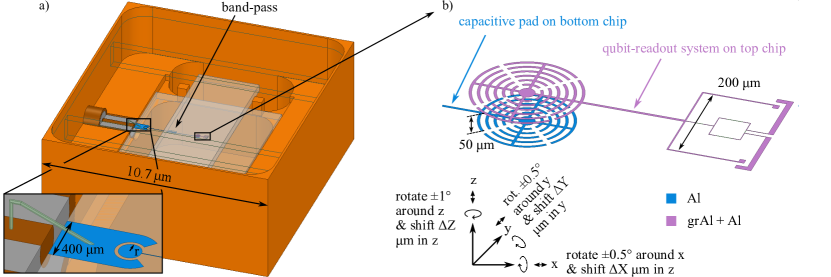
Appendix A Finite element simulations
To investigate the influence of qubit chip misalignment, mismatch between readout and band-pass filter frequency and the contribution of the copper box to energy relaxation, we perform eigenmode simulations with the finite element solver Ansys HFSS. We run the simulations in a detailed 3D model of a single enclosure that is shown in Fig. A1. The simulations are terminated at a convergence error of less than 1 % and are based on the parameters of qubit 1. We model the pure grAl parts in the QR system with lumped inductors, i.e. nH, fF and nH. The qubit mode is simulated as a harmonic mode which is why we replace the JJ with a lumped capacitor fF resulting in a resonance frequency of GHz.
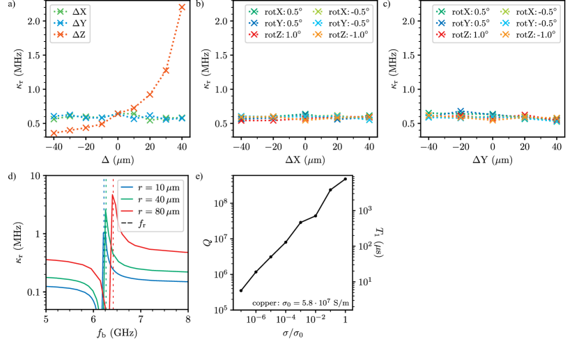
To analyze the architecture susceptibility to misalignment, we simulate the bandwidth of the readout mode for a qubit chip that is shifted and rotated in X, Y & Z directions. The results are shown in Fig. A2.a,b,c. In Fig. A2.d, we show the dependence of on the band-pass frequency and the capacitive coupling strength to the rf-port (expressed by the radius of the circular capacitance). To assess the contribution of the box to the qubit energy relaxation time, we simulate the quality factor of a mode that includes the JJ for increasing losses in the copper box, i.e. we reduce the conductivity of the simulated sample box material. To calculate the qubit from the simulated , we use Fermi’s Golden Rule
| (A1) |
where is the inductive energy, the flux operator in units of , and the qubit frequency. The simulated and calculated values are shown in Fig. A2.e and exceed s for copper indicating that at the moment these losses are not a limiting factor.
Appendix B Sample fabrication
The qubit chips are fabricated using e-beam lithography and shadow evaporation. The Josephson junction and the capacitive structures are a result of an aluminum double-angle evaporation with an intermediate static oxidation process for the junction insulating barrier. The inductive parts are implemented with granular aluminum wires, deposited with a zero-angle aluminum evaporation in combination with a dynamical oxygen flow in the evaporation chamber. The patterning and deposition is conducted in a single lithographic and evaporation step and follows the recipe from Ref. [26]. In summary the deposition process is started at a pressure below mbar with a plasma cleaning step using a Kaufman source (200 V, 10 mA, 10 sccm , 5 sccm Ar) that is followed by a titanium evaporation with a closed shutter (10 s at 0.2 nm/s). The fist aluminum layer is evaporated at a angle (20 nm at 1 nm/s) and then statically oxidized at 50 mbar for 4 minutes. The second aluminum layer is deposited at a angle (30 nm at 1 nm/s), followed by argon milling step at (400 V, 15 mA, 4 sccm Ar) to ensure contact to the final 70 nm thick granular aluminum layer (evaporated with 2 nm/s at a 0° angle with a -flow of 9.4 sccm and planetary rotation at 5 rpm).
The capacitive extenders ( mm) that each span half the qubit chip length, pose an additional fabrication challenge, as they increase the risk of electric discharge during resist spinning or chip dicing processes. As visible in Fig. A3, destroyed junctions can be directly related to electric discharge induced by the extenders that capacitively couple the junction electrodes to the chip edges. This problem is remedied by shunting the junction with a low impedance aluminum film, which is etched away after the final dicing process.
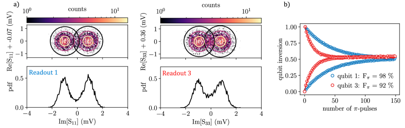
Appendix C Readout and single qubit gate fidelity
We show simultaneous readout and single qubit -pulse calibration measurements in Fig. A4. The readout pulse lengths are equal to the integration time s, which is on the order of the qubit relaxation time. As visible from the overlapping pointer state distributions and absence of additional states in Fig. A4a, qubit relaxation during readout is the main limitation of the single shot readout separation fidelity. The -pulse is calibrated as a Gaussian envelope pulse with ns pulse length. We show sequences of subsequently played -pulses in Fig. A4b. The abscence of beating patterns proves an optimal power calibration. We define the -pulse fidelity via the exponential decay versus the pulse sequence length and find and for qubit 1 and qubit 3, respectively, which is limited by qubit relaxation.
Appendix D Power calibration
Following Ref. [31], the dephasing rate added to qubit when driving the microwave line connected to port at frequency with amplitude is given by
| (A2) |
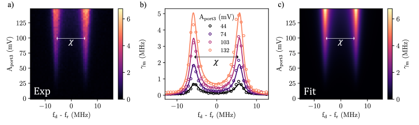
where , are the resonance frequency and the linewidth of the resonator coupled to qubit via the dispersive shift , which is defined as the frequency difference of the readout resonator frequency when the qubit is in the ground or the excited state, respectively. The two terms in the parenthesis correspond to the circulating photon number in the resonator for the qubit in the ground and excited state. The microwave field amplitude seen by resonator is related to via the power transfer coefficient : . Accordingly, we define the port-to-resonator isolation on a logarithmic power scale as .
We measure for various and via Ramsey interferometry. As an example, the data for when driving through port 3 is shown in Fig. A5a. In Fig. 3.b in the main text, we report values for and for . For each , we fit the data to Eq. A2 using the fitting parameters , , and , as shown in Fig. A5b. This yields different values of for different amplitudes, giving a measure of the uncertainty in the extraction of . In Fig. A5c, we show the calculated dephasing using the mean values of the fitted parameters. By comparing the dephasing of qubit 1 and qubit 3 while driving through port 3, we extract .
Appendix E Measurements of qubit-qubit avoided crossings
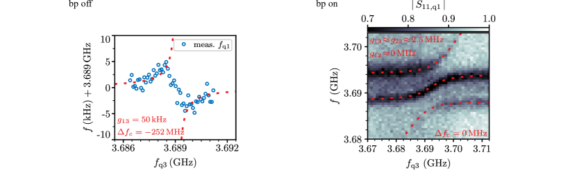
In Fig. A6 and Fig. A7 we show the measured avoided level splittings between qubits 1 and 3 for for different coupler detunings , which are used in Fig. 4 in the main text. Measurement data for MHz is obtained by performing two-tone spectroscopy on qubit 1. At the idle point (MHz) we measure Ramsey fringes on q1 to characterize the avoided level splitting.
Appendix F Schrieffer-Wolff transformation
In this appendix, we provide a detailed explanation of the calculations that result in the theoretical prediction for the effective qubit-qubit coupling shown in Fig. 4 of the main text. These calculations are based on two different applications of the Schrieffer-Wolff transformation [34, 43] (SWT) to the superconducting circuit, composed of three unit cells, shown in Fig. 1 g). Both SWTs yield an effective two-qubit model that captures how the coupling between qubits in e1 and e3 depends on the detuning of the qubit in e2 (coupler). The two SWTs complement each other: the first is exact and fully relies on the numerical methods developed in Ref. [33, 44] (continuous line in Fig. 4), while the second uses a semi-analytical approach that gives us a qualitative understanding of the mediated coupling (dashed line in Fig. 4).
The circuit under study can be decomposed into three sub-circuits, or unit cells, that are capacitively coupled. As shown in Fig. 1g, this involves a direct coupling between sub-circuits 1 and 2 through capacitor , between sub-circuits 2 and 3 through capacitor , and an indirect coupling between sub-circuits 1 and 3 through the sample box, . As discussed in Ref. [26], each of the sub-circuits under study can be modeled as a flux qubit and a resonator inductively coupled, however, this inductive coupling can be neglected in the treatment below, because during the experiment the qubits are far detuned from their respective resonators. We use a Hamiltonian of three capacitively coupled flux qubits:
| (A3) | ||||
where , and are the Hamiltonian, the linear inductance and the Josephson energies of qubit [26]. The symbols are the elements of the inverse of the capacitance matrix . The non-diagonal elements of couple different flux qubits. All single qubit parameters in Eq. A3 are determined by fitting the flux-dependent spectra obtained for the qubits in the experiments, as shown in App. G.
In the following, we explain how to derive an effective model that describes the coupling between qubits 1 and 3 as a function of the frequency of the coupler qubit. That is, we map the Hamiltonian of the full circuit shown in Eq. A3 to an effective one of the form
| (A4) |
where is the renormalized frequency of qubit , slightly shifted from the frequency of the bare qubits, and are the coupling strengths in the different directions.
Let us assume a Hamiltonian that can be decomposed in an unperturbed part plus a perturbation, . The SWT is a unitary transformation of the Hamiltonian that decouples an eigensubspace of interest (the two-qubit subspace) of the interacting model from the rest of the Hilbert space through a unitary map to the equivalent eigensubspace of the non-interacting problem . If we call the projectors onto the qubit eigensubspace with and without interactions and , and the complementary eigensubspace projectors and , the SWT maps those projectors, , and . It has been shown [43] that
| (A5) |
With the SWT we can obtain an effective Hamiltonian that describes the dynamics of our coupled two-qubit subspace as
| (A6) |
Note that this procedure is valid whenever the subspaces and are gapped from the rest of the spectrum regardless of whether they involve low energy states or not.
In this manuscript we use the SWT in two strategies to derive an effective Hamiltonian in the low-energy subspace of the first and third qubits. In the first and more complete strategy our starting point is the full circuit mode Hamiltonian Eq. A3, while in the second one we start from an effective model of three coupled qubits and apply the SWT in a perturbative fashion.
In the first approach, we rely on a numerically exact procedure [33] which allows us to work directly with the circuit Hamiltonian Eq. A3. Here, our unperturbed Hamiltonian is the sum of the bare Hamiltonians of the flux qubits that appear in Eq. A3, that is, , and the perturbation is the capacitive coupling between them, . Since we are interested in the effective coupling between qubits 1 and 3, our subspace of interest will include the eigenstates that have up to one excitation in either qubit 1 or 3, with zero excitations in the coupler qubit, that is, . The projector is composed of the numerically estimated eigenstates of that correspond to the same qubit subspace. From and , using the procedure introduced in Ref. [33] we arrive at the effective Hamiltonian
| (A7) |
Experimentally, we characterize the effective coupling strength by half the energy splitting between the one excitation eigenstates, solid points shown in Fig. 4. To obtain this energy difference we diagonalize the Hamiltonian above, which can be written as a matrix
| (A8) |
Assuming that qubits 1 and 3 are on resonance, the energy splitting is directly given by , corresponding to the solid line in Fig. 4. Furthermore, as evidenced by our numerical simulations, , a quantity below our experimental resolution, see Fig. 3c.
In the second approach, we derive an analytical approximation for the energy splitting . Following Ref. [44] we start from a model of three capacitively coupled qubits in the limit in which the coupler qubit is highly detuned
| (A9) |
This model is derived by projecting the coupled flux qubit Hamiltonian Eq. A3 onto the non-interacting subspace of the three qubits, . Here are the qubit gaps of the bare model. The interaction is derived from the projection of the capacitive coupling .
Similar to Ref. [45], we implement an analytical SWT using perturbative series up to second order with , and, . The second-order expansion of the effective Hamiltonian includes the projection of the perturbed Hamiltonian onto our subspace of interest and the virtual transitions mediated by excited states
| (A10) |
As qubits 1 and 3 are on resonance in the experiment, , we recover the effective Hamiltonian
| (A11) |
with the renormalized qubit gaps
| (A12) |
and the interaction
| (A13) |
Since in this case there is no term proportional to the coupling corresponds directly to the measured energy splitting, and is shown as a dotted line in Fig. 4. In the equations above we have defined and Note that this second order expansion presents divergences that are absent in the complete SWT [43].
Let us emphasize that the SWT on the full quantum circuit is numerically exact and describes the three interacting qubits without approximations (except for possible crosstalks or couplings that are not considered in the circuit). In contrast, the analytical SWT is based on an effective pairwise model that only captures the dominant contributions to the final coupling, exhibits non-existent divergences and cannot reflect phenomena such as interaction mediated by excited states or perturbative couplings between the qubits.
Appendix G Qubit parameters
We model the single qubit spectra using the flux qubit Hamiltonian and neglecting the resonator:
| (A14) |
where and are the qubit flux and charge operators, is the external flux applied to the qubit loop and , and are the qubit capacitance, inductance and the junction Josephson energy. These three parameters are fitted to spectroscopic measurements. The fits are plotted in Fig. A8 and the fit results are summarized in Table A1.
The flux qubit coherence is typically best at half flux bias, aka sweet spot, due to the first order insensitivity to flux noise. To operate the qubits on resonance, however, qubit 3 is detuned from its respective sweet spot to match the frequency of qubit 1, at the expense of coherence. The energy relaxation times and Ramsey coherence times for the qubits and the coupler are summarized in Table A1. The frequency , bandwidth and loaded quality factor of the devices readout resonators are listed in Table A2.
| device | [GHz] | [nH] | [fF] | @ [GHz] | @ [s] | @ [s] | @ bp [s] | @ bp [s] |
|---|---|---|---|---|---|---|---|---|
| qubit 1 | 6.2 | 22.1 | 32.2 | 3.689 | 2.1 | 1.7 | – | – |
| coupler | 9.6 | 20.2 | 22.7 | 3.437 | – | – | – | – |
| qubit 3 | 5.6 | 31.6 | 25.2 | 3.084 | 1.7 | 1.1 | 0.8 | 0.17 |
| device | @ [GHz] | [MHz] | |
|---|---|---|---|
| readout 1 | 6.508 | 2.2 | 3000 |
| rout-coupler | 6.274 | 4.2 | 1500 |
| readout 3 | 5.226 | 1.3 | 3900 |
Appendix H Qubit-qubit population transfer
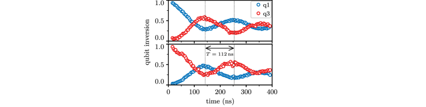
To demonstrate population transfer via the tunable coupler, we use the fast flux bias line to tune the coupler from the idle point to the bias point with a baseband rectangular pulse of variable length and subsequently read out both qubits simultaneously. Preparing either qubit 1 or 3 in the excited state with a pulse yields oscillations in the qubit populations as shown in Fig. A9. The extracted swap time is ns which is consistent with the effective qubit-qubit coupling strength of 2.5 MHz obtained via spectroscopy. The transfer fidelity is likely limited by the coherence time of qubit 2 and 3, which both operate off the sweet spot when the coupling is switched on.
Appendix I Scaling in 2 dimensions
To upgrade the one-dimensional array in two dimensions, the rf- and dc-ports of the enclosures need to be repositioned. As illustrated in Fig. A10, access to the enclosures is gained through out-of-plane feedthroughs which couple capacitively to the control chips and are wire-bonded to the coupler chips. As coupling element, an all-to-all reconfigurable router similar to [46] could be used.