Tuning of Josephson junctions - the effects of depinning physics
Abstract
Building more powerful quantum computers requires manufacturing processes with tight tolerances. To improve the tolerances on Josephson junctions, techniques to fine tune their properties after fabrication have been developed. Understanding how tuning techniques may physically modify the tunnel barrier of a Josephson junction is important and will enable these techniques to be optimised. We develop a model of junction tuning based on depinning theory to interpret a phase diagram of tuning rate. We extract the dependence on temperature, time varying voltages and oscillation frequency. Using depinning theory we are able to show both why time varying annealing potentials result in controlled junction tuning and how such protocols can be optimised. We examine how tuning changes the electrical breakdown of barriers and discrepancies between modeled and measured higher energy levels of transmon qubits.
Quantum computers with high qubit count, low error rates and error correcting protocols promise new computational capabilities. Processors comprised of superconducting qubits are a leading platform for utility scale quantum computation [1, 2, 3] but building these at scale and with high quality poses many challenges, several of which lie in the processor manufacture. One such component which poses manufacturing difficulties is the Josephson junction (JJ). These are most often based on stacks of Al/AlOx/Al and are typically made by shadow angle evaporation [4] where a bottom layer of thin-film aluminium is oxidised before being coated by a second layer of aluminium. Uncontrolled variation in as-fabricated JJs currently limit qubit frequency assignment accuracy to 1 % [5, 6, 7], insufficiently precise for high fidelity 2Q gates in some gate modalities [8, 9]. Not only are junctions challenging to make with tight tolerance, but their properties change over time after their manufacture in a process known as aging [10] which complicates processor design. In order to address this variation a family of techniques which allow post-manufacture parameter adjustment have been developed including modifying the junction by laser irradiation [9, 11], electron beam irradiation [12] and the application of alternating bias at elevated temperatures [13].
In this article we introduce a refined bias protocol using a lock-in amplifier, which naturally incorporates alternating bias [13]. The lock-in allows for fast measurements of resistance at variable frequencies allowing precise resistance targetting even with large tuning speed. We explore the voltage-temperature-frequency space of the tuning process and interpret the resultant phase diagram with a depinning model. We find good agreement between this model and the three-dimensional phase diagram. We compare tuned and untuned junctions measuring both breakdown voltages and Josephson harmonics [14].
We build a setup shown schematically in Fig. 1 (a) where we connect a JJ in series with a load resistor, creating a potential divider, and connect this circuit between the output ports of a Zurich Instruments MFLI lock-in amplifier. Measuring the voltage drop across either of these elements allows us to infer the resistance of the JJ, the property we optimise in this process. We can control both the amplitude and the frequency of the AC voltage output from the lock-in amplifier. The sample containing JJs is placed on a Peltier heating stage to control the temperature of the JJ during this process.
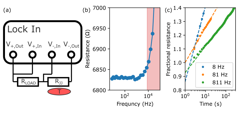
We measure the resistance of the JJ as a function of the lock-in frequency (Fig. 1 b) and find that we get constant values up to a frequency of 8 kHz, when the measured resistance increases. This increase in resistance is a measurement artefact due to RC filtering based on a computed cut-off frequency of 40 kHz, with most capacitance arising from coaxial cabling 111Using a series resistance of 15 k and a typical capacitance for BNC cables of 80pF/m. Considering 3m of cables, we compute an RC frequency of 44 kHz.. We confine our frequency operating window to frequencies below 1 kHz to ensure we infer the correct resistances of the JJs.
In Fig. 1 (c) we show how resistance changes during the tuning protocol for three frequencies; 8 Hz, 81 Hz and 811 Hz. We fit these tuning curves phenomenologically to a model where the resistance increases logarithmically with time
| (1) |
where is the resistance at the start of the protocol and both and are fit parameters, with relating to the speed of tuning. We find this model fits all measured tuning curves well, and that tuning increases in speed with decreasing frequency. On some occasions, not shown in Fig. 1, the junction fails during the tuning process, becoming a short circuit. The rate of junction failures for a given process is another parameter we explore.
We show that the behaviour (speed and failure rate) of junctions undergoing voltage tuning can be understood in terms of depinning theory. Depinning theory applies to a wide range of systems in which there is an interplay between disorder, temperature and applied stresses. This is seen in domain walls in magnets, the movement of vortices in superconductors, charge movement in Josephson junction arrays, dislocation movement, crack formation and even the formation of avalanches in sand piles [16, 17, 18, 19, 20].
The classic picture of depinning theory as applied to disordered media invokes two phases, a pinned static phase where the system is in a relaxed local minima and a sliding phase where local regions or domains within the system have a nonzero average velocity [21, 22]. In the pinned phase, any static or oscillating field can induce local microscopic changes, which can act as a dissipation channel [23], but not large scale movement or restructure. Above some threshold applied field (the ‘depinning threshold’) the movement of these local domains has some finite average velocity and can ultimately lead to avalanche behaviour.
In the presence of an applied field, localised regions within the material can move or reposition. These domains are referred to as “elastic objects”, and can be localised defects, phase boundaries, vortices or other objects depending on the particular material being considered. The characteristic size of these objects is given by the Larkin length () - also known as the Imry-Ma or Fukuyama-Lee length - which is the scale at which the pinning forces due to disorder and the elastic forces are comparable [21]. At this length scale the movement of an elastic object can be thought of as a single degree of freedom and we can consider the movement of these collective domains through the material. Interestingly, this means that the exact microscopic details are unimportant and simply set the value of characteristic parameters in the theory. As we will show, the tuning of junctions with an oscillating voltage is well described by this picture, even though it does not explicitly allow us to differentiate between the various models of defects or domains within the junction [23, 24, 25].
We consider the junction dielectric to host domains which are trapped local minima. Applying sufficient field or temperature can move these domains, surmounting some effective potential barrier. Following Nattermann et al. [22], we define the depinning temperature where the thermal energy is equivalent to the barrier height. The depinning voltage is the point at which there is sufficient applied field for domains to continuously move through the material, resulting in an avalanche.
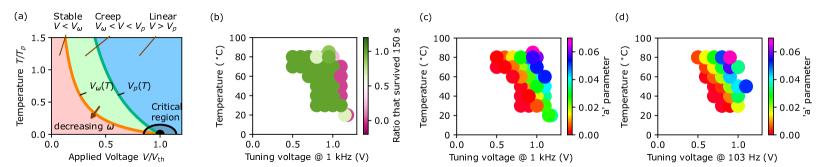
The regions of interest in a generic depinning theory are illustrated in Fig. 2 (a). The linear response or ‘running’ region (blue shaded area) applies for constant fields greater than the temperature dependent depinning voltage . Any constant applied field less than this will not result in a significant change in the structure of the material, it will be ‘pinned’ (the red shaded area). The zero temperature limit of can be taken as the breakdown voltage .
The general depinning threshold separating these two regions is defined by the relation
| (2) |
where is a constant which depends on the effective dimensionality of the elastic object (for 1-2 dimensional domains in a 3D medium, it can be approximated to 1) and is a critical exponent for the depinning transition which is but is non-universal and will depend on the microscopic details of the system [22].
When an oscillatory field is applied, a 3rd regime is formed in the phase diagram. The so-called ‘creep’ region (green region of Fig. 2 a) is the region in which domains can most easily move during the oscillatory field annealing process. In the creep region, the oscillating field results in hysteretic behaviour, i.e., the velocity can initially be directed in the opposite direction to the applied field - see Refs [26, 17] for details.
The creep threshold is a function of the field oscillation frequency via
| (3) |
where depends on the oscillation frequency and the characteristic timescale required for a domain to overcome the barrier to move from its local equilibrium.
Of particular interest for understanding the junction tuning results, a) if the creep region is larger for lower frequencies, and b) in the creep regime, there is a linear movement of defects without leading to full avalanche. This explains why lower frequencies result in greater resistance shifts for fixed values of temperature and voltage amplitude, the creep region grows as the frequency is reduced. At some low-frequency-limit we anticipate this trend stops, as domain movement saturates before the field polarity is reversed presenting a new energy landscape to the mobile domains. We can also understand the junction breakdown in terms of the depinning avalanche process for , which is both temperature and local disorder realisation dependent.
To confirm our interpretation in terms of depinning theory we tune junctions with varying voltage and temperature at frequencies of both 1 kHz and 103 Hz. For each parameter set we tune at least three junctions. We fit each of these tuning curves to Eq. 1 and extract the speed parameter . We also compute how many junctions fail prior to 150 s of tuning process. We present this data as a function of temperature and voltage amplitude, Fig. 2 (b). A clear boundary is observed at a tuning voltage of V which is consistent with the measured mean breakdown voltage of V (see Fig. 3 c). We therefore associate this boundary with the depinning threshold .
We then compare this threshold to the tuning ‘speed’ parameter in Eq. 1. Operating at 1 kHz, we vary the temperature and voltage amplitude of the tuning process. In Fig. 2 (c) we plot , finding a similar boundary, now at a lower voltage, consistent with the expected behaviour of . This process is then repeated at a different tuning frequency (103 Hz) with data shown in Fig. 2 (d). Again showing the expected increase in the creep regime with reducing frequency, implying s.
To fit the boundaries between regimes quantitatively requires estimates for , , , and and a better understanding of the relationship between depinning velocity and the tuning speed parameter. We can estimate from junction breakdown measurements at a given temperature. Some indications for the depinning temperature can be given by observations of where the rate of thermal aging starts to increase. To give an indication of likely temperature scales, in [27, 28, 29] changes are first seen C and large scale junction modification is observed at C in [30, 31, 32, 33].
The phase diagram in Fig. 2 (a) indicates sharp lines demarking regions of the phase diagram. However, increases smoothly with increasing voltage, starting at 0. Likewise, the onset of junction failure starts with a small subset of junctions failing, increasing to all junctions failing at higher voltage. Operationally these boundaries are ‘fuzzy’ which is consistent with the disorder realisation dependent nature of the depinning process. As a result, considerations weighing process time against yield can be used to select a working point.
Mapping out this phase diagram we have identified room temperature working points with appreciable process speed. This offers multiple advantages, key among them is that junctions which are not tuned undergo no heating and associated aging, a significant benefit for processor design. The exact mechanism of the tuning, as well as the nature of the domains being depinned, is currently unknown. More detailed mapping of the phase diagram, combined with the statistics of many junctions, will provide invaluable data to compare to potential models of junction tuning.
Having demonstrated creep behaviour in our junctions, we compare junction properties before and after tuning to expand this understanding. Following our recent work [34] we measure the electrical breakdown of junctions by ramping a DC voltage across these junctions from 0 to 1.7 V recording the current that flows through each junction as a function of voltage (Fig. 3 a). We fit the linear portion of this IV to extract the resistance of the JJ. At some voltage the junction fails and becomes short circuit which is recorded as the breakdown voltage (black star in Fig. 3 a). We compare two sets of junctions, distinguished by their tuning, with resistances shown in Fig. 3 (b). The first set of 20 junctions is tuned at 85 ∘C with a voltage of 0.92 V targeting 30 % total tuning and find an average tuning of 34.6 0.8 %. This systematic overshoot occurs due to continued resistance changes over time, after we have hit our target value, as shown in Ref. 35. During this process two junctions failed. The second set of 25 junctions are fabricated on the same chip, undergo the same 85 ∘C heating as the tuned junctions, but are not tuned by an alternating voltage. Despite undergoing no electrical tuning they are 4 % higher in resistance than the junctions before tuning due to the thermal processing they undergo, indicative of why a room temperature process is advantageous.
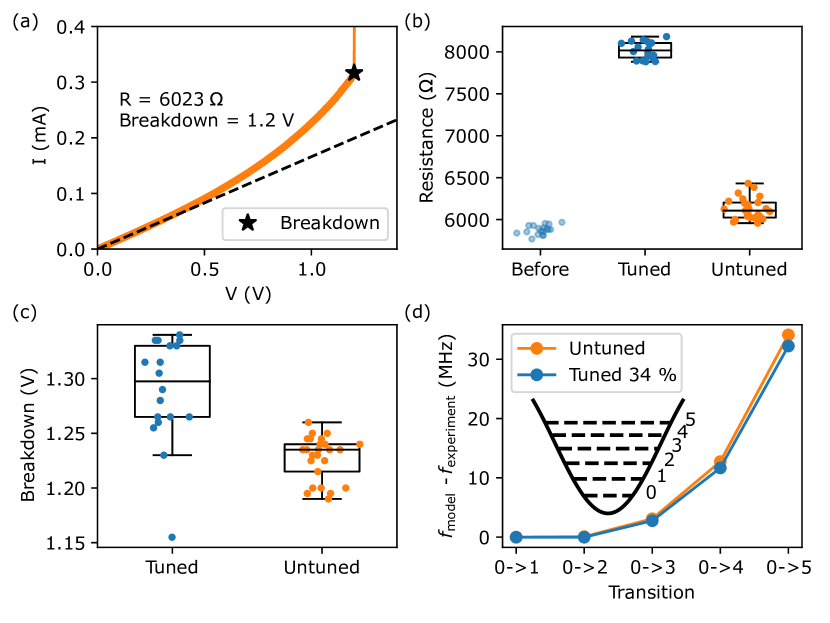
In Fig. 3 (c) we show that on average junctions which have undergone tuning have a larger breakdown voltage, increasing by 5 %. However, despite the increase in average breakdown voltage, the lowest breakdown voltage recorded was from a junction that had undergone tuning. The breakdown voltage is given by
| (4) |
where is the local thickness of the barrier and is the local dielectric strength of the barrier. Both of these values may, in principle, vary across the barrier [36, 37]. In our recent work [34] we show that by assuming constant , we can model the standard deviation of breakdown voltages by assuming it occurs at the thinnest points in the barrier. This does not describe a bimodal distribution which we see in a large-N study of untuned junctions. Based on this study, we cautiously interpret these results as an increase in the minimum barrier thickness after tuning of the junction. Given typical barrier thicknesses of 2 nm, a 5 % change in thickness represents 0.1 nm, less than the typical ionic diameter in these solids [38]. In the depinning model we describe above domains are mobile under the application of electric fields. These fields will be the strongest at the thinnest regions of the barrier which means that the the creep rate will also be greatest at these thinnest points. Such weak points in the barrier have been suggested to contribute to non-idealities [37, 14, 39] and breakdown [40] of the JJs. An approach that reduces the non-idealities associated to pin holes or weak points may have advantages in homogenising the current phase relations of junctions.
The higher-energy states of transmon qubits have recently been suggested to be sensitive to the nanostructure of the barrier in JJs [14]. In Fig. 3 (d) we show the results of measuring two coaxmon qubits [41] where one qubit has had a junction tuned by 34 % and the other has experienced the same thermal treatment but not been tuned. The results of Ref. 14 would suggest that by substantially modifying the barrier we might expect to see some difference to the frequencies of these higher levels. We follow the protocol from Ref. 42, treating the coaxmon as a qudit and tuning up a series of gates across the 6 energy levels shown schematically in Fig. 3 (d). We compute the Josephson energy and charging energy using qutip [43] by considering the first two transition frequencies and constraining them to match the results from the transmon Hamiltonian
| (5) |
where and are the charge and phase operators respectively and and are the charging and Josephson energies [44]. The tuned (untuned) coaxmon have junction resistances of 5802 (6021 ), charging energies of 166 MHz (168 MHz) and Josephson energies of 23.2 GHz (22.2 GHz). In Fig. 3 (d) we show the difference between the measured transition frequencies and the computed transition frequencies for the different qudit states for both a tuned and untuned coaxmon. We find there is no substantial difference between the two coaxmons.
By mapping out the voltage-temperature-frequency phase diagram of tuning under oscillatory bias we have shown that the tuning process is qualitatively described by depinning theory. The domains within the amorphous oxide barrier creep between local minima driven by both temperature and the oscillating field. Depinning theory by itself does not point to a particular origin of these local domains, as it is consistent with small scale defects [24], movement of grain boundaries [25] or other microscopic models [23]. Nonetheless by interpreting the results in terms of depinning theory, the working point can be chosen to improve the junction tuning protocol, choosing how deeply into the creep-region one wishes to operate. We find a set of parameters that allow junction tuning at room temperature with appreciable speed, where untuned junctions are also not subject to heating and associated modifications.
We show that tuning modifies, not only the resistance of the junctions, but also the breakdown voltage of the junctions. Together these could be explained by an increase in the thickness of the barrier at its thinnest points. We contrast this to a measurement of ‘Josephson Harmonics’ which appear unchanged comparing tuned and untuned junctions. The interpretation in Ref. 14 suggests that deviations in these harmonics can be ascribed to the thinnest points of junctions. Taken together our measurements suggest that the depinning process modifying the junction resistance is not simply ‘filling in’ the thinnest points of barriers, but fundamentally modifies the junction microstructure. Reconciling these observations will allow a deeper understanding of what constitutes domains in these junctions.
Acknowledgements.
We extend our thanks to the OQC Fabrication team for discussions relating to this work and the OQC Hardware team for developments across the stack which enabled these measurements. The authors thank Dave Pappas for useful discussions. The authors thank Peter Leek and Jonathan Burnett for reviewing this manuscript. Computational resources were provided by the Australian National Computational Infrastructure facility (NCI). We thank the Royal Holloway University of London SuperFab Facility for their support.References
- Arute et al. [2019] F. Arute, K. Arya, R. Babbush, D. Bacon, J. C. Bardin, R. Barends, R. Biswas, S. Boixo, F. G. Brandao, D. A. Buell, et al., Quantum supremacy using a programmable superconducting processor, Nature 574, 505 (2019).
- Chow et al. [2021] J. Chow, O. Dial, and J. Gambetta, Ibm quantum breaks the 100-qubit processor barrier, IBM Research Blog 2 (2021).
- AI [2023] G. Q. AI, Suppressing quantum errors by scaling a surface code logical qubit, Nature 614, 676 (2023).
- Kreikebaum et al. [2020] J. Kreikebaum, K. O’Brien, A. Morvan, and I. Siddiqi, Improving wafer-scale josephson junction resistance variation in superconducting quantum coherent circuits, Superconductor Science and Technology 33, 06LT02 (2020).
- Osman et al. [2023] A. Osman, J. Fernández-Pendás, C. Warren, S. Kosen, M. Scigliuzzo, A. Frisk Kockum, G. Tancredi, A. Fadavi Roudsari, and J. Bylander, Mitigation of frequency collisions in superconducting quantum processors, Physical Review Research 5, 043001 (2023).
- Acharya et al. [2024] N. Acharya, R. Armstrong, Y. Balaji, K. G. Crawford, J. C. Gates, P. C. Gow, O. W. Kennedy, R. D. Pothuraju, K. Shahbazi, and C. D. Shelly, Integration of through-sapphire substrate machining with superconducting quantum processors, Advanced Materials , 2411780 (2024).
- Van Damme et al. [2024] J. Van Damme, S. Massar, R. Acharya, T. Ivanov, D. Perez Lozano, Y. Canvel, M. Demarets, D. Vangoidsenhoven, Y. Hermans, J. Lai, et al., Advanced cmos manufacturing of superconducting qubits on 300 mm wafers, Nature , 1 (2024).
- Morvan et al. [2022] A. Morvan, L. Chen, J. M. Larson, D. I. Santiago, and I. Siddiqi, Optimizing frequency allocation for fixed-frequency superconducting quantum processors, Physical Review Research 4, 023079 (2022).
- Hertzberg et al. [2021] J. B. Hertzberg, E. J. Zhang, S. Rosenblatt, E. Magesan, J. A. Smolin, J.-B. Yau, V. P. Adiga, M. Sandberg, M. Brink, J. M. Chow, et al., Laser-annealing josephson junctions for yielding scaled-up superconducting quantum processors, npj Quantum Information 7, 129 (2021).
- Koppinen et al. [2007a] P. Koppinen, L. Väistö, and I. Maasilta, Complete stabilization and improvement of the characteristics of tunnel junctions by thermal annealing, Applied physics letters 90 (2007a).
- Kim et al. [2022] H. Kim, C. Jünger, A. Morvan, E. S. Barnard, W. P. Livingston, M. Altoé, Y. Kim, C. Song, L. Chen, J. M. Kreikebaum, et al., Effects of laser-annealing on fixed-frequency superconducting qubits, Applied Physics Letters 121 (2022).
- Balaji et al. [2024] Y. Balaji, N. Acharya, R. Armstrong, K. G. Crawford, S. Danilin, T. Dixon, O. W. Kennedy, R. D. Pothuraju, K. Shahbazi, and C. D. Shelly, Electron-beam annealing of josephson junctions for frequency tuning of quantum processors, arXiv preprint arXiv:2402.17395 (2024).
- Pappas et al. [2024] D. P. Pappas, M. Field, C. J. Kopas, J. A. Howard, X. Wang, E. Lachman, J. Oh, L. Zhou, A. Gold, G. M. Stiehl, et al., Alternating-bias assisted annealing of amorphous oxide tunnel junctions, Communications Materials 5, 150 (2024).
- Willsch et al. [2024] D. Willsch, D. Rieger, P. Winkel, M. Willsch, C. Dickel, J. Krause, Y. Ando, R. Lescanne, Z. Leghtas, N. T. Bronn, et al., Observation of josephson harmonics in tunnel junctions, Nature Physics , 1 (2024).
- Note [1] Using a series resistance of 15 k and a typical capacitance for BNC cables of 80pF/m. Considering 3m of cables, we compute an RC frequency of 44 kHz.
- Wiese [2022] K. J. Wiese, Theory and experiments for disordered elastic manifolds, depinning, avalanches, and sandpiles, Reports on Progress in Physics 85, 086502 (2022).
- Brazovskii and Nattermann [2004] S. Brazovskii and T. Nattermann, Pinning and sliding of driven elastic systems: from domain walls to charge density waves, Advances in Physics 53, 177 (2004).
- Vogt et al. [2014] N. Vogt, R. Schäfer, H. Rotzinger, W. Cui, A. Fiebig, A. Shnirman, and A. V. Ustinov, One-dimensional Josephson junction arrays: Lifting the Coulomb blockade by depinning, Physical Review B 92 (2014).
- Vogt et al. [2016] N. Vogt, J. H. Cole, and A. Shnirman, De-pinning of disordered bosonic chains, New Journal of Physics 18, 053026 (2016).
- Cedergren et al. [2017] K. Cedergren, R. Ackroyd, S. Kafanov, N. Vogt, A. Shnirman, and T. Duty, Insulating Josephson Junction Chains as Pinned Luttinger Liquids, Physical Review Letters 119, 167701 (2017).
- Middleton and Fisher [1991] A. A. Middleton and D. S. Fisher, Critical behavior of pinned charge-density waves below the threshold for sliding, Physical Review Letters 66, 92 (1991).
- Nattermann et al. [2001] T. Nattermann, V. Pokrovsky, and V. M. Vinokur, Hysteretic Dynamics of Domain Walls at Finite Temperatures, Physical Review Letters 87, 197005 (2001).
- Müller et al. [2019] C. Müller, J. H. Cole, and J. Lisenfeld, Towards understanding two-level-systems in amorphous solids: insights from quantum circuits, Reports on Progress in Physics 82, 124501 (2019).
- Strand and Shluger [2024] J. Strand and A. L. Shluger, On the structure of oxygen deficient amorphous oxide films, Advanced Science 11, 2306243 (2024).
- Oh et al. [2025] J.-S. Oh, C. J. Kopas, H. Cansizoglu, J. Y. Mutus, K. Yadavalli, T.-H. Kim, M. Kramer, A. H. King, and L. Zhou, Correlating aluminum layer deposition rates, josephson junction microstructure, and superconducting qubits’ performance, Acta Materialia 284, 120631 (2025).
- Schütze and Nattermann [2011] F. Schütze and T. Nattermann, Mean-field theory for driven domain walls in disordered environments, Physical Review B 83, 024412 (2011).
- Imamura et al. [1992] T. Imamura, T. Shiota, and S. Hasuo, Fabrication of high quality nb/alo/sub x/-al/nb josephson junctions. i. sputtered nb films for junction electrodes, IEEE Transactions on Applied Superconductivity 2, 1 (1992).
- Oliva and Monaco [1994] A. Oliva and R. Monaco, Annealing properties of high quality nb/al-alo/sub x//nb tunnel junctions, IEEE Transactions on Applied Superconductivity 4, 25 (1994).
- Migacz and Huber [2003] J. Migacz and M. Huber, Thermal annealing of nb/al-alo/sub x//nb josephson junctions, IEEE Transactions on Applied Superconductivity 13, 123 (2003).
- Pop et al. [2012] I. M. Pop, T. Fournier, T. Crozes, F. Lecocq, I. Matei, B. Pannetier, O. Buisson, and W. Guichard, Fabrication of stable and reproducible submicron tunnel junctions, Journal of Vacuum Science & Technology B 30 (2012).
- Julin et al. [2010] J. K. Julin, P. J. Koppinen, and I. J. Maasilta, Reduction of low-frequency 1/f noise in al–alox–al tunnel junctions by thermal annealing, Applied Physics Letters 97, 152501 (2010).
- Koppinen et al. [2007b] P. J. Koppinen, L. M. Väistö, and I. J. Maasilta, Complete stabilization and improvement of the characteristics of tunnel junctions by thermal annealing, Applied Physics Letters 90, 053503 (2007b).
- Korshakov et al. [2024] N. D. Korshakov, D. O. Moskalev, A. A. Soloviova, D. A. Moskaleva, E. S. Lotkov, A. R. Ibragimov, M. V. Androschuk, I. A. Ryzhikov, Y. V. Panfilov, and I. A. Rodionov, Aluminum josephson junction microstructure and electrical properties modification with thermal annealing, arXiv preprint arXiv:2403.02179 (2024).
- Kennedy et al. [2025] O. W. Kennedy, K. G. Crawford, K. Shahbazi, and C. D. Shelly, Analysis of josephson junction barrier variation – a combined stem, breakdown and monte-carlo approach, arXiv preprint arXiv:2502.13072 (2025).
- Wang et al. [2024a] X. Wang, J. Howard, E. A. Sete, G. Stiehl, C. Kopas, S. Poletto, X. Wu, M. Field, N. Sharac, C. Eckberg, et al., Precision frequency tuning of tunable transmon qubits using alternating-bias assisted annealing, arXiv preprint arXiv:2407.06425 (2024a).
- Cyster et al. [2020] M. J. Cyster, J. S. Smith, J. A. Vaitkus, N. Vogt, S. P. Russo, and J. H. Cole, Effect of atomic structure on the electrical response of aluminum oxide tunnel junctions, Physical Review Research 2, 013110 (2020).
- Bayros et al. [2024] K. Bayros, M. Cyster, J. Smith, and J. Cole, Influence of pinholes and weak-points in aluminum-oxide josephson junctions, Physical Review Materials 8, 046202 (2024).
- Dobrovinskaya et al. [2009] E. R. Dobrovinskaya, L. A. Lytvynov, and V. Pishchik, Properties of sapphire, Sapphire , 55 (2009).
- Greibe et al. [2011] T. Greibe, M. P. V. Stenberg, C. M. Wilson, T. Bauch, V. S. Shumeiko, and P. Delsing, Are ”pinholes” the cause of excess current in superconducting tunnel junctions? A study of Andreev current in highly resistive junctions, Physical Review Letters 106, 1657 (2011).
- Tolpygo and Amparo [2008] S. K. Tolpygo and D. Amparo, Electrical stress effect on Josephson tunneling through ultrathin AlOx barrier in Nb/Al/AlOx/Nb junctions, Journal of Applied Physics 104, 063904 (2008).
- Rahamim et al. [2017] J. Rahamim, T. Behrle, M. Peterer, A. Patterson, P. Spring, T. Tsunoda, R. Manenti, G. Tancredi, and P. Leek, Double-sided coaxial circuit qed with out-of-plane wiring, Applied Physics Letters 110 (2017).
- Wang et al. [2024b] Z. Wang, R. W. Parker, E. Champion, and M. S. Blok, Systematic study of high transmon qudits up to , arXiv preprint arXiv:2407.17407 (2024b).
- Johansson et al. [2012] J. R. Johansson, P. D. Nation, and F. Nori, Qutip: An open-source python framework for the dynamics of open quantum systems, Computer physics communications 183, 1760 (2012).
- Koch et al. [2007] J. Koch, T. M. Yu, J. Gambetta, A. A. Houck, D. I. Schuster, J. Majer, A. Blais, M. H. Devoret, S. M. Girvin, and R. J. Schoelkopf, Charge-insensitive qubit design derived from the cooper pair box, Physical Review A—Atomic, Molecular, and Optical Physics 76, 042319 (2007).