Multifield Induced Antiferromagnet Transformation into Altermagnet and Realized Anomalous Valley Hall Effect in Two-dimensional Materials
Abstract
Altermagnetism, as a new category of collinear magnetism distinct from traditional ferromagnetism and antiferromagnetism, exhibits the spin splitting without net magnetization. Currently, researchers are focus on searching three-dimensional altermagnetism and exploring its novel physical properties. However, there is a lack of understanding of the physical origin of two-dimensional altermagnetic emergent behavior. Here, we propose an approach to realize the transition from Neel antiferromagnetism to altermagnetism in two-dimensional system using an electric field, Janus structure, and ferroelectric substrate. In monolayer VPSe3, we demonstrate that multiple-physical-fields cause the upper and lower Se atoms unequal to break PT symmetry, resulting in altermagnetic spin splitting. Noted that monolayer VPSe3 produces a spontaneous valley splitting of 2.91 meV at the conduction band minimum. The electric field can effectively tune the valley splitting magnitude, while the Janus structure not only changes the valley splitting magnitude, but also alters the direction. More interestingly, when the ferroelectric polarization of Al2S3 is P, the direction of valley polarization is switched and the magnitude is almost unchanged. However, the valley splitting significantly increases under the P. It is worth noting that the ferroelectric polarization can switch altermagnetic effect and realize anomalous valley Hall effect. Besides, we reveal the microscopic mechanism of valley splitting by an effective Hamiltonian. Our findings not only provide a method to designing altermagnet, but also enriches the valley physics.
I Introduction
Recently, a new type of magnetism named ”altermagnetism” has been proposed in condensed matter physics 1 ; 2 ; 3 ; 4 ; 5 . The altermagnetism has two fascinating properties, which mainly manifested as a zero net magnetic moment and spin splitting along specific high symmetry paths without the spin-orbit coupling (SOC). The discovery has not only promoted the development of spintronics, but also enriched the application scenarios of magnetic materials. For example, giant and tunneling magnetoresistance effect is raised in altermagnets 6 . Besides, the anomalous Hall effect is reported in the altermagnet RuO2, which the magnitude can be compared to that of ferromagnet (FM) 7 . In addition, a new type of torque, spin splitter torque, has been theoretically proposed 8 and experimentally observed 9 ; 10 in the altermagnet. Moreover, the heterojunctions of altermagnet are reported to possess chiral Majorana Fermion or Majorana zero energy modes 11 ; 12 . However, these investigations have mainly focused on bulk materials 2 ; 3 ; 4 ; 5 ; 6 ; 7 ; 8 ; 9 ; 10 ; 13 ; 14 ; 15 ; 16 , while two-dimensional (2D) altermagnets pay limited attention. How to tune the 2D antiferromagnet (AFM) into altermagnet is even less involved. But it is crucial to understanding the origin of the emergent behavior.
In spintronics, a new degree of freedom, valley, has been proposed as the third degree of freedom beyond the electron’s charge and spin 17 ; 18 ; 19 ; 20 . The valley indicates a local energy minimum or maximum point in the conduction or valence band. At present, the investigation focus of valleytronics is how to realize spontaneous valley polarization and effectively tune 21 ; 22 ; 23 ; 24 ; 25 ; 26 ; 27 ; 28 ; 29 . There are two main ways to achieve spontaneous valley polarization, which is named ferrovalley material 21 . One approach is to break the time-reversal symmetry (T) with the FM or AFM 21 ; 22 ; 23 ; 24 ; 25 ; 29 , while the other way is to break the inversion symmetry (P) by ferroelectricity 27 ; 28 ; 30 . It is well known that altermagnets break the combined symmetry of the P and T (named the PT symmetry). Whether the altermagnetism can realize spontaneous valley polarization, and how it differs from the FM and AFM systems?
In this work, we propose a new scheme for achieving altermagnetism in 2D system. Here, we focus on the transformation of AFM into altermagnet by the multifield induction, such as an electric field, Janus structure, and ferroelectric substrate. It is well known that the AFM hold the PT symmetry. The multiple-physical-fields can induce the PT symmetry breaking, which causes the band degeneracies of spin up and spin down bands to disappear on special high symmetrical path, exhibiting altermagnetic characteristics. Based on the density functional theory (DFT) calculations, we demonstrate this mechanism and phenomena in monolayer VPSe3. Moreover, monolayer VPSe3 exhibits spontaneously valley polarization due to the combined effects of SOC and T symmetry breaking. The electric field can effectively tune the magnitude of valley splitting, while the Janus structure (built-in electric field) and ferroelectric substrate can regulate not only the magnitude but also the direction and position of valley polarization. In addition, the ferroelectric polarization can switch altermagnetic effect and realize anomalous valley Hall effect. Our work provide a new direction for investigating altermagnetism and valleytronic devices.
II STRUCTURES AND COMPUTATIONAL METHODS
Based on the framework of the DFT, we employed the Vienna simulation package (VASP) 31 ; 32 to investigate the electronic and magnetic properties. The generalized gradient approximation (GGA) with the Perdew-Burke-Ernzerhof (PBE) functional is used to describe the exchange correlation energy 33 . The kinetic energy cutoff for plane-wave basis is set to be 500 eV. A vacuum of 30 is added along the c-axis, to avoid the interaction between the sheet and its periodic images. The convergence criteria of the total energy and the force for lattice optimization are set to 10-6 eV and -0.005 eV/, respectively. To describe strongly correlated 3d electrons of V, the GGA+U approach is performed with the effective U value (Ueff = U - J) of 3 eV 34 . The zero damping DFT-D3 approach of Grimme is considered for the van der Waals (vdW) correction in VPSe3/Al2S3 heterostructure 35 . In addition, to study the Berry curvature, the maximally localized Wannier functions (MLWFs) are used to construct an effective tight-binding Hamiltonian by Wannier90 code 36 ; 37 .
III RESULTS AND DISCUSSION
IV RESULTS AND DISCUSSION
IV.1 Structure and symmetry
As shown in Fig. 1(a), it shows the crystal structure of monolayer VPSe3, which is six Se atom nearest to each V atom. The monolayer VPSe3 shows a hexagonal honeycomb lattice with the point group of D3d and space group of P1m. The optimized lattice constant of VPSe3 is 6.24 . When magnetic order isn’t considered, monolayer VPSe3 has the P symmetry. However, since the magnetic ground state of VPSe3 is Nel AFM, both the P and T symmetry are broken. Despite this, it exhibits invariance when the spatial inversion and time reversal occur simultaneously, that is, the PT symmetry (see Fig. 1(b)). It is well established that a system with PT symmetry exhibits Kramers degeneracy in its band structure. Namely, as shown in Fig. 1(c), the spin up and spin down bands are degenerate. Besides, the opposite spin sublattices are jointed by the combined rotation and mirror symmetry, denoted as [C2M]. The [C2M] symmetry lead to E(s, k) = [C2M]E(s, k) = E(-s, Mk), which plays a vital role in realizing altermagnetism. Here, the s, k, and E(s, k) represent the spin, momentum, and spin- and momentum-dependent bands, respectively.
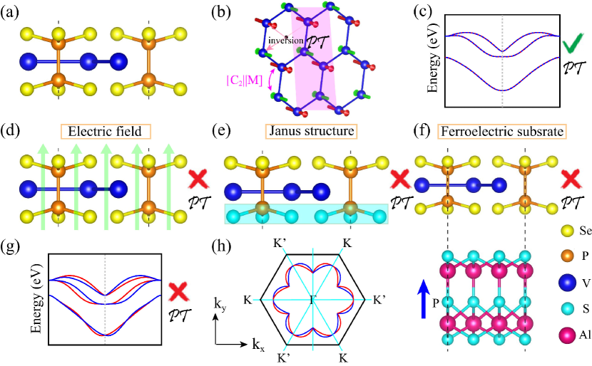
Here, we propose three kinds of field to break the PT symmetry. As shown in Fig. 1(d-f), these include the application of out-of-plane external electric fields, the functionalizing crystal structure into Janus configuration form by substituting the bottom Se layer through S atoms, and the applied ferroelectric substrate. A common feature of these three methods is that the mirror symmetry can be preserved. Consequently, as shown in Fig. 1(g), the Kramers degeneracy is lifted, and the band structure characteristics of altermagnet are exhibited. More interestingly, as shown in Fig. 1(h), the i-wave altermagnets are formed.
IV.2 Band structure and valley splitting
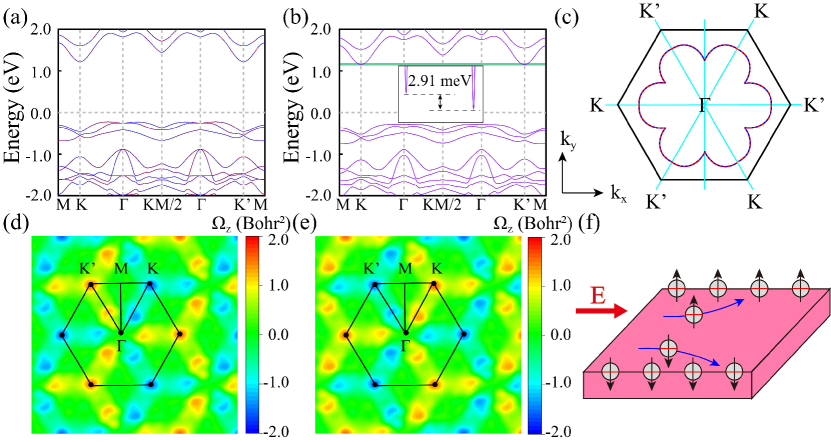
To determine the magnetic ground state of monolayer VPSe3, the two most likely magnetic configurations including the FM and Neel type AFM are considered (the Neel Type AFM is hereinafter referred to as AFM). We calculate that the FM state is 277.67 meV more energy than the AFM state, which indicates that the AFM phase is the magnetic ground state of monolayer VPSe3. For the 2D magnetic materials, the out-of-plane magnetic anisotropy energy (MAE) is the basis for their stable existence 38 ; 39 . The MAE is defined as MAE = E100 - E001, where E100 and E001 represent the total energy of the magnetic moment along [100] and [001] axis, respectively. The calculated MAE is 0.10 meV, which indicates the easy magnetization direction along the [001] axis.
Then, we calculate the spin-polarized band structure of monolayer VPSe3. As shown in Fig. 2(a), the spin up and spin down bands are degenerate, which the PT symmetry induces the Kramers degeneracy. It is worth noting that the K/K’ valley of conduction band minimum (CBM) is degenerate. Noted that Fig. 2(c) plots the valence band at around -1.2 eV. When the SOC is switched on, as shown in Fig. 2(b), the energy valley degeneracy of K and K’ disappears, resulting in 2.91 meV spontaneous valley splitting. Here, we define valley splitting as the energy difference between K and K’ points. The origin of valley splitting in monolayer VPSe3 is consistent with the previously reported magnetic system due to the combined T symmetry broken and SOC effect. To understand the orbital composition of valley splitting, we calculate the orbital-resolved band structure of monolayer VPSe3. As shown in Fig. S1, the valence band maximum (VBM) bands are mainly contributed by the d+dxy+d orbitals of V atoms, while the CBM bands are dominated by the px+py orbitals of Se atoms.
To understand the origin of valley splitting in monolayer VPSe3, we employed cτ=(px+ipy) as the orbital basis to build an effective Hamiltonian. The = 1 represent the valley index referring to the K/K’ point. Taken the SOC effect as a perturbation term, the effective Hamiltonian can be written as
| (1) |
where and are spin and orbital angular operators, respectively. The and denote the interaction between the same spin states and between opposite spin states, respectively. In monolayer VPSe3, we only consider the interaction between spin up states. Thus, the term can be neglected. Accordingly, the can be rewritten by polar angles
| (2) |
When the easy magnetization axis is along the out-of-plane, = = 0∘, then the term can be reduced as
| (3) |
Therefore, the energy level of the CBM valley can be written as Ecτ = cτ cτ . Consequently, the valley splitting can be described as
| (4) |
where the = i, = -i.
In addition, we understand valleys in terms of Berry curvature. Since monolayer AFM VPSe3 is protected by PT symmetry, the Berry curvature is zero for the entire Brillouin zone. Therefore, we calculate the Berry curvature of spin up and spin down states. As shown in Fig. 2(d, e), the Berry curvature has equal magnitude at the K and K’ points, while it shows opposite signs for the same valley of different spin states and different valleys of the same spin state. When the Fermi level shifts the conduction band of K’ valley by electron doping, the spin up electrons from K’ valley will be accumulated at the right edge of the sample, while the spin down electrons from K’ valley will shift to the left edge under an in-plane electric field. As shown in Fig. 2(f), we name the phenomenon the spin-valley Hall effect.
IV.3 Electric field induce transformation into altermagnet
From the perspective of device applications, the electric field stands out as the most effective means for tuning the physical quantity 40 ; 41 . This modulation method not only responds swiftly but also avoids causing damage to the materials themselves, demonstrating unique advantages in the application of micro- and nano-devices. Therefore, we investigate the effect of electric field on monolayer VPSe3. Here, instead of re-optimizing VPSe3 structure, we apply an electrostatic potential to monolayer VPSe3. This causes the upper and lower Se atomic layer to be inequivalent, resulting in the broken PT symmetry. In the absence the SOC effect, the band structure holds sixfold rotational symmetry (C6). The E(s, k) = E(-s, -k) relationship is satisfied on special high symmetric lines. However, the rotational symmetry of band structure will be reduced to threefold (C3) under the SOC effect.
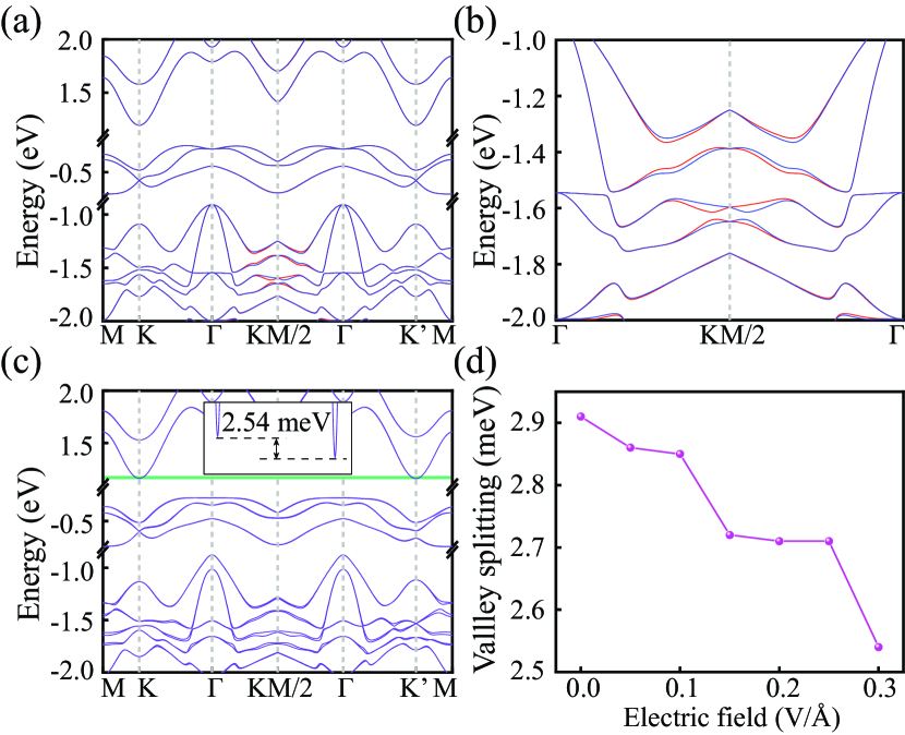
Firstly, we investigate the magnetic ground state at the 0.0 0.3 V/. As shown in Fig. S2, the effect of electric field on the energy difference between FM and AFM states is only 0.1 meV, which means that the AFM phase is still the magnetic ground state. To confirm the symmetry analysis, we calculate the band structure at an electric field of 0.3 V/. As shown in Fig. 3(a), both valence and conduction bands of the valley at K and K’ points is completely degenerate, which verifies that the band structure has C6 symmetry without the SOC effect. More interestingly, as shown in Fig. 3(b), the spin splitting exhibits at the -KM/2- path. It is the typical characteristic of altermagnet, which the AFM material doesn’t has. Moreover, when the SOC is included, the valley splitting of 2.54 meV is still observed at the CBM. Since the valley degeneracy of K and K’ points disappears, the symmetry decreases from the C6 to C3. It also demonstrates our symmetry analysis. Besides, as shown in Fig. 3(d), the change of valley splitting is only 0.4 meV at the 0.0 0.3 V/. It is mainly because the splitting valley is contributed by the non-magnetic Se atom.
IV.4 Janus structure induce transformation into altermagnet
The second approach is that it actually makes the upper and lower Se atomic layers unequal. We use S atom to replace lower Se atom to form the Janus structure V2P2S3Se3. To enrich the physical properties of 2D materials, Zhang et al. has successfully prepared Janus graphene as early as 2013 42 . After more than ten years of development, the current technology for preparing 2D Janus structures has been very mature and successfully synthesized Janus transition metal dichalcogenides (TMDs), such as MoSSe 43 , WSSe 44 , Janus MXenes 45 etc. Due to the asymmetry between the lower and upper surfaces of the Janus structure, a significant built-in electric field is produced. Therefore, it naturally breaks the PT symmetry. We speculate that the same phenomenon of VPSe3 applied electric field will be generated in V2P2S3Se3.
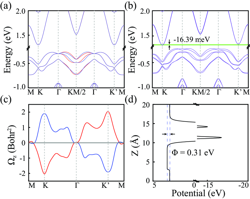
In the absence of SOC, as shown in Fig. 4(a), the significant spin splitting is clearly observed in the -KM/2- path. It indicates that the AFM to altermagnet transition is realized by constructing the Janus structure without the PT symmetry. In addition, the CBM at the K and K’ points exhibits valley degeneracy. When the SOC is switched on, as illustrated in Fig. 4(b), the K and K ’valley degeneracies disappear, producing valley splitting up to -16.39 meV. It demonstrates that the intrinsic spontaneous valley polarization is achieved in the altermagnet monolayer V2P2S3Se3. Besides, to understand the valley related physics, we calculate Berry curvature of the monolayer V2P2S3Se3. As shown in Fig. 4(c), the Berry curvature of spin up exhibits a negative value near the K point and a positive near the K’ point. On the contrary, the Berry curvature of spin down is completely reversed sign. It is also the characteristic of valley degeneracy. To further understand the valley splitting of monolayer V2P2S3Se3 -16.39 meV, we introduce the built-in electric field Ein = ( - )/, where , , and represent the electrostatic potential at the upper surface and lower surface, and structural height of V2P2S3Se3, respectively. As shown in Fig. 4(d), the built-in electric field is 0.10 V/ by the electrostatic potential. The built-in electric field of 0.10 V/ not only significantly increases the valley splitting, but also changes its sign. Why is the regulation effect of 0.10 V/ built-in electric field on valley splitting much better than that of external electric field. The important reason is the difference in SOC strength between S and Se atoms, which the S and Se atoms are 1.8 meV and 4.0 meV, respectively.
IV.5 Ferroelectric substrate induce transformation into altermagnet
A third method to achieve altermagnets is by constructing heterostructures, which the heterostructure is naturally broken PT symmetry. In order to explore the regulation of substrate on valley splitting, we choose the ferroelectric substrate Al2S3 and VPSe3 to form heterostructure. The lattice constant of Al2S3 is 3.59 . We find that the lattice mismatch rate of the 1 1 unit cell of VPSe3 matching the Al2S3 is only 0.3 . As shown in Fig. 5(a, e) and Fig. S3, four typical configurations are considered: top-S, top-Al, bridge, and hollow configuration. As listed in Table SI, the layer spacing in all configurations is 3.24 3.82 , which indicates the interlayer is typically weak vdW interaction. In addition, all configurations exhibit an out-of-plane MAE, as listed in Table SII. From the relative total energy in Table SIII, the top-S, and top-Al are the most stable P and P configurations, respectively.
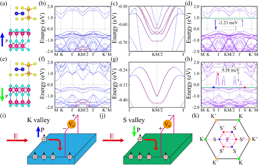
In the following, we take top-S configuration as an example for detailed analysis. When the ferroelectric polarization of Al2S3 is P, the spin-polarized band structure is illustrated in Fig. 5(b). The VBM and CBM are located at K- path and K/K’ point, simultaneously, the CBM of K and K’ points exhibit valley degeneracy. When the P switches P, as shown in Fig. 5(f), the CBM becomes the M point, while the VBM remains on the K- path. Very interestingly, the valley of VBM shows degeneracy, which is not a high symmetric point. Most importantly, as shown in Fig. 5(c, g), both P and P configurations produce spin splitting. This confirms the feasibility of our mechanism for realizing altermagnet. When the SOC is included, Fig. 5(d) shows the band structure of P. The valley polarization direction is tuned by the Al2S3, however, the magnitude has barely changed. When the ferroelectric polarization of Al2S3 becomes P, as shown in Fig. 5(h), the valley splitting of 9.58 meV occurs at the VBM.
To understand the origin of VBM and CBM valley splitting, as shown in Fig. S6, we calculate the orbital-resolved band structure of top-S configuration VPSe3/Al2S3. The CBM valley splitting comes from the Se atom liked monolayer VPSe3, while the VBM valley splitting is contributed by d+dxy of V atoms. We uses vτ=(dxy+idx2-y2) as the orbital basis to construct an effective Hamiltonian. The derivation is consistent. Here, we only give the conclusion.
| (5) |
where the = -2i, = 2i, and .
It should be pointed out that the valley-dependent spin splitting occurs with the lower symmetry and SOC. Therefore, the anomalous valley Hall effect will be observed. As shown in Fig. 5(i), the spin down electron of K valley will be generated and accumulate on one boundary in electron doping condition for the P. On the contrary, in the hole doping case, the spin up hole of S valley will also be produced and accumulate on same boundary for the P [see Fig. 5(j)]. Furthermore, Fig. 5(k) shows the location of valley splits under two polarization states in the first Brillouin zone. All configurations of valley splitting are listed in Table I. Noted that the same phenomenon appears for other configurations, as shown in Fig. S4 and Fig. S5. It means that ferroelectric substrate Al2S3 can effectively tune the direction and magnitude of VPSe3 valley polarization. More interestingly, the ferroelectric polarization can switch altermagnetism effect, which indicates the ferroelectric polarization is coupled to the altermagnetic spin splitting.
| top-S | top-Al | hollow | bridge | |
|---|---|---|---|---|
| VPSe3/Al2S3 P (meV) | -2.23 | -3.45 | -3.13 | -2.82 |
| VPSe3/Al2S3 P (meV) | 9.58 | 9.15 | 8.74 | 8.96 |
V CONCLUSION
In summary, we present a novel strategy to realizing altermagnet in 2D material. We use an electric field, Janus structure, and ferroelectric substrate to make the upper and lower atoms asymmetric, while the PT symmetry of the AFM state is broken, resulting in a transition to altermagnetic state. Based on the symmetry analysis and DFT calculation, the mechanism is proved to be feasible in monolayer VPSe3. The magnetic ground state of monolayer VPSe3 is an AFM state, which exhibits a spontaneous valley splitting of 2.91 meV. The electric field, the Janus structure, and the ferroelectric substrate can effectively break the PT symmetry, so that the band structure can exhibit spin splitting at the -KM/2- path. It proves that multiple-physical-fields can transform monolayer VPSe3 from AFM to altermagnetic state. Moreover, the electric field can adjust the magnitude of valley splitting, while the Janus structure can regulate both the magnitude and direction of valley splitting. For the ferroelectric substrate Al2S3, the valley polarization direction is effectively tuned and the magnitude hardly changes under the P. However, when the ferroelectric polarization of Al2S3 switches from P to P, the valley splitting significantly increases. In addition, the ferroelectric polarization can switch altermagnetic effect and realize anomalous valley Hall effect. Our work not only provides a route to realize the altermagnet in 2D system, but also an efficient ways to tune valley splitting.
ACKNOWLEDGEMENTS
This work is supported by the National Natural Science Foundation of China (Grants No. 12474238, and No. 12004295). P. Li also acknowledge supports from the China’s Postdoctoral Science Foundation funded project (Grant No. 2022M722547), the Fundamental Research Funds for the Central Universities (xxj03202205), and the Open Project of State Key Laboratory of Silicon and Advanced Semiconductor Materials (No. SKL2024-10), and the Open Project of State Key Laboratory of Surface Physics (No. KF202402).
References
- (1) H. Y. Ma, M. Hu, N. Li, J. Liu, W. Yao, J. F. Jia, and J. Liu, Multifunctional antiferromagnetic materials with giant piezomagnetism and noncollinear spin current, Nat. Commun. 12, 2846 (2021).
- (2) L. Smejkal, J. Sinova, and T. Jungwirth, Beyond conventional ferromagnetism and antiferromagnetism: A phase with nonrelativistic spin and crystal rotation symmetry, Phys. Rev. X 12, 031042 (2022).
- (3) L. Smejkal, J. Sinova, and T. Jungwirth, Emerging Research Landscape of Altermagnetism, Phys. Rev. X 12, 040501 (2022).
- (4) Y. P. Zhu, X. Chen, X. R. Liu, Y. Liu, P. Liu, H. Zha, G. Qu, C. Hong, J. Li, Z. Jiang, X. M. Ma, Y. J. Hao, M. Y. Zhu, W. Liu, M. Zeng, S. Jayaram, M. Lenger, J. Ding, S. Mo, K. Tanaka, M. Arita, Z. Liu, M. Ye, D. Shen, J. Wrachtrup, Y. Huang, R. H. He, S. Qiao, Q. Liu, and C. Liu, Observation of plaid-like spin splitting in a noncoplanar antiferromagnet, Nature, 626, 523 (2024).
- (5) J. Krempasky, L. Smejkal, S. W. DSouza, M. Hajlaoui, G. Springholz, K. Uhlirova, F. Alarab, P. C. Constantinou, V. Strocov, D. Usanov, W. R. Pudelko, R. G. Hernandez, A. B. Hellenes, Z. Jansa, H. Reichlova, Z. Soban, R. D. G. Betancourt, P. Wadley, J. Sinova, D. Kriegner, J. Minar, J. H. Dil, and T. Jungwirth, Altermagnetic lifting of Kramers spin degeneracy, Nature, 626, 517 (2024).
- (6) L. Smejkal, A. B. Hellenes, R. G. Hernandez, J. Sinova, and T. Jungwirth, Giant and tunneling magnetoresistance in unconventional collinear antiferromagnets with nonrelativistic spin-momentum coupling, Phys. Rev. X 12, 011028 (2022).
- (7) Z. Feng, X. Zhou, L. Smejkal, L. Wu, Z. Zhu, H. Guo, R. G. Hernandez, X. Wang, H. Yan, P. Qin, X. Zhang, H. Wu, H. Chen, Z. Meng, L. Liu, Z. Xia, J. Sinova, T. Jungwirth, and Z. Liu, An anomalous Hall effect in altermagnetic ruthenium dioxide, Nat. Electron. 5, 735 (2022).
- (8) R. G. Hernandez, L. Smejkal, K. Vyborny, Y. Yahagi, J. Sinova, T. Jungwirth, and J. Zelezny, Efficient Electrical Spin Splitter Based on Nonrelativistic Collinear Antiferromagnetism, Phys. Rev. Lett. 126, 127701 (2021).
- (9) S. Karube, T. Tanaka, D. Sugawara, N. Kadoguchi, M. Kohda, and J. Nitta, Observation of spin-splitter torque in collinear antiferromagnetic RuO2, Phys. Rev. Lett. 129, 137201 (2022).
- (10) H. Bai, L. Han, X. Y. Feng, Y. J. Zhou, R. X. Su, Q. Wang, L. Y. Liao, W. X. Zhu, X. Z. Chen, F. Pan, X. L. Fan, and C. Song, Observation of spin splitting torque in a collinear antiferromagnet RuO2, Phys. Rev. Lett. 128, 197202 (2022).
- (11) S. A. A. Ghorashi, T. L. Hughes, and J. Cano, Altermagnetic Routes to Majorana Modes in Zero Net Magnetization, Phys. Rev. Lett. 133, 106601 (2024).
- (12) H. G. Giil, and J. Linder, Superconductor-altermagnet memory functionality without stray fields, Phys. Rev. B 109, 134511 (2024).
- (13) X. Zhou, W. Feng, R. W. Zhang, L. Smejkal, J. Sinova, Y. Mokrousov, and Y. Yao, Crystal Thermal Transport in Altermagnetic RuO2, Phys. Rev. Lett. 132, 056701 (2024).
- (14) J. Ding, Z. Jiang, X. Chen, Z. Tao, Z. Liu, T. Li, J. Liu, J. Sun, J. Cheng, J. Liu, Y. Yang, R. Zhang, L. Deng, W. Jing, Y. Huang, Y. Shi, M. Ye, S. Qiao, Y. Wang, Y. Guo, D. Feng, and D. Shen, Large Band Splitting in g-Wave Altermagnet CrSb, Phys. Rev. Lett. 133, 206401 (2024).
- (15) Z. Q. Wang, Z. Q. Li, L. Sun, Z. Y. Zhang, K. He, H. Niu, J. Cheng, M. Yang, X. Yang, G. Chen, Z. Yuan, H. F. Ding, and B. F. Miao, Inverse Spin Hall Effect Dominated Spin-Charge Conversion in (101) and (110)-Oriented RuO2 Films, Phys. Rev. Lett. 133, 046701 (2024).
- (16) L. Bai, W. Feng, S. Liu, L. Sejkal, Y. Mokrousov, and Y. Yao, Altermagnetism: Exploring New Frontiers in Magnetism andSpintronics, Adv. Funct. Mater. 34, 2409327 (2024).
- (17) D. Xiao, W. Yao, and Q. Niu, Valley-Contrasting Physics in Graphene: Magnetic Moment and Topological Transport, Phys. Rev. Lett. 99, 236809 (2007).
- (18) T. Cao, G. Wang, W. Han, H. Ye, C. Zhu, J. Shi, Q. Niu, P. Tan, E. Wang, B. Liu, and J. Feng, Valley-selective circular dichroism of monolayer molybdenum disulphide, Nat. Commun. 3, 887 (2012).
- (19) K. F. Mak, K. He, J. Shan, and T. F. Heinz, Control of valley polarization in monolayer MoS2 by optical helicity, Nat. Nanotechnol. 7, 494 (2012).
- (20) H. Zeng, J. Dai, W. Yao, D. Xiao, and X. Cui, Valley polarization in MoS2 monolayers by optical pumping, Nat. Nanotechnol. 7, 490 (2012).
- (21) W. Y. Tong, S. J. Gong, X. Wan, and C. G. Duan, Concepts of ferrovalley material and anomalous valley Hall effect, Nat. Commun. 7, 13612 (2016).
- (22) R. Peng, Y. Ma, X. Xu, Z. He, B. Huang, and Y. Dai, Intrinsic anomalous valley Hall effect in single-layer Nb3I8, Phys. Rev. B 102, 035412 (2020).
- (23) K. Wang, Y. Li, H. Mei, P. Li, and Z. X. Guo, Quantum anomalous Hall and valley quantum anomalous Hall effects in two-dimensional d0 orbital XY monolayers, Phys. Rev. Mater. 6, 044202 (2022).
- (24) P. Li, C. Wu, C. Peng, M. Yang, and W. Xun, Multifield tunable valley splitting in two-dimensional MXene Cr2COOH, Phys. Rev. B 108, 195424 (2023).
- (25) P. Li, X. Yang, Q. S. Jiang, Y. Z. Wu, and W. Xun, Built-in electric field and strain tunable valley-related multiple topological phase transitions in VSiXN4(X = C, Si, Ge, Sn, Pb) monolayers, Phys. Rev. Mater. 7, 064002 (2023).
- (26) P. Li, B. Liu, S. Chen, W. X. Zhang, and Z. X. Guo, Progress on two-dimensional ferovalley materials, Chin. Phys. B 33, 017505 (2024).
- (27) Y. Wu, J. Tong, L. Deng, F. Luo, F. Tian, G. Qin, and X. Zhang, Coexisting Ferroelectric and Ferrovalley Polarizations in Bilayer Stacked Magnetic Semiconductors, Nano Lett. 23, 6226 (2023).
- (28) W. Xun, C. Wu, H. Sun, W. Zhang, Y. Z. Wu, and P. Li, Coexisting Magnetism, Ferroelectric, and Ferrovalley Multiferroic in Stacking-Dependent Two-Dimensional Materials, Nano Lett. 24, 3541 (2024).
- (29) S. D. Guo, L. Zhang, Y. Zhang, P. Li, and G. Wang, Large spontaneous valley polarization and anomalous valley Hall effect in antiferromagnetic monolayer Fe2CF2, Phys. Rev. B 110, 024416 (2024).
- (30) X. W. Shen, W. Y. Tong, S. J. Gong, and C. G. Duan, Electrically tunable polarizer based on 2D orthorhombic ferrovalley materials, 2D Mater. 5, 011001 (2017).
- (31) P. E. Blochl, Projector augmented-wave method, Phys. Rev. B 50, 17953 (1994).
- (32) G. Kresse, and J. Furthmuller, Efficient iterative schemes for ab initio total-energy calculations using a plane-wave basis set, Phys. Rev. B 54, 11169 (1996).
- (33) J. P. Perdew, K. Burke, and M. Ernzerhof, Generalized Gradient Approximation Made Simple, Phys. Rev. Lett. 77, 3865 (1996).
- (34) H. P. Wang, W. Luo, and H. J. Xiang, Prediction of high-temperature quantum anomalous Hall effect in two-dimensionaltransition-metal oxides, Phys. Rev. B 95, 125430 (2017).
- (35) S. Grimme, J. Antony, S. Ehrlich, and H. Krieg, A consistent and accurate ab initio parameterization of density functional dispersion correction (DFT-D) for the 94 elemenets H-Pu, J. Chem. Phys. 132, 154104 (2010).
- (36) A. A. Mostofi, J. R. Yates, Y. S. Lee, I. Souza, D. Vanderbilt, and N. Marzari, wannier90: A tool for obtaining maximally-localised Wannier functions, Commput. Phys. Commun. 178, 685 (2008).
- (37) A. A. Mostofi, J. R. Yates, G. Pizzi, Y. S. Lee, I. Souza, D. Vanderbilt, and N. Marizari, An updated version of wannier90: A tool for obtaining maximally-localised Wannier functions, Commput. Phys. Commun. 185, 2309 (2014).
- (38) C. Gong, L. Li, Z. Li, H. Ji, A. Stern, Y. Xia, T. Cao, W. Bao, C. Wang, Y. Wang, Z. Q. Qiu, R. J. Cava, S. G. Louie, J. Xia, and X. Zhang, Discovery of intrinsic ferromagnetism in two-dimensional van der Waals crystals, Nature, 546, 265 (2017).
- (39) B. Huang, G. Clark, E. N. Moratalla, D. R. Klein, R. Cheng, K. L. Seyler, D. Zhong, E. Schmidgall, M. A. McGuire, D. H. Cobden, W. Yao, D. Xiao, P. J. Herrero, and X. Xu, Layer-dependent ferromagnetism in a van der Waals crystal down to the monolayer limit, Nature 546, 270 (2017).
- (40) Q. Lu, P. Li, Z. Guo, G. Dong, B. Peng, X. Zha, T. Min, Z. Zhou, and M. Liu, Giant Tunable Spin Hall Angle in Sputtered Bi2Se3 Controlled by an Electric Field, Nat. Commun. 13, 1650 (2022).
- (41) P. Li, X. S. Zhou, and Z. Guo, Intriguing Magnetoelectric Effect in Two-dimensional Ferromagnetic Perovskite Oxide Ferroelectric Heterostructure, npj Comput. Mater. 8, 20 (2022).
- (42) L. Zhang, J. Yu, M. Yang, Q. Xie, H. Peng, and Z. Liu, Janus graphene from asymmetric two-dimensional chemistry, Nat. Commun. 4, 1443 (2013).
- (43) A. Y. Lu, H. Zhu, J. Xiao, C. P. Chuu, Y. Han, M. H. Chiu, C. C. Cheng, C. W. Yang, K. H. Wei, Y. Yang, Y. Wang, D. Sokaras, D. Nordlund, P. Yang, D. A. Muller, M. Y. Chou, X. Zhang, and L. J. Li, Janus monolayers of transition metal dichalcogenides, Nat. Nanotechnol. 12, 744 (2017).
- (44) Y. C. Lin, C. Liu, Y. Yu, E. Zarkadoula, M. Yoon, A. A. Puretzky, L. Liang, X. Kong, Y. Gu, A. Strasser, H. M. Meyer III, M. Lorenz, M. F. Chisholm, I. N. Ivanov, C. M. Rouleau, G. Duscher, K. Xiao, and D. B. Geohegan, Low Energy Implantation into Transition-Metal Dichalcogenide Monolayers to Form Janus Structures, ACS Nano 14, 3896 (2020).
- (45) H. Tang, W. Li, L. Pan, K. Tu, F. Du, T. Qiu, J. Yang, C. P. Cullen, N. McEvoy, C. Zhang, and A Robust, Freestanding MXene-Sulfur Conductive Paper for Long-Lifetime Li-S Batteries, Adv. Funct. Mater. 29, 1901907 (2019).